EP2372917A1 - Gerät zur parallelen Analog-Digital-Wandlung und ein solches Gerät umfassender Bildgebungsdetektor - Google Patents
Gerät zur parallelen Analog-Digital-Wandlung und ein solches Gerät umfassender Bildgebungsdetektor Download PDFInfo
- Publication number
- EP2372917A1 EP2372917A1 EP11305327A EP11305327A EP2372917A1 EP 2372917 A1 EP2372917 A1 EP 2372917A1 EP 11305327 A EP11305327 A EP 11305327A EP 11305327 A EP11305327 A EP 11305327A EP 2372917 A1 EP2372917 A1 EP 2372917A1
- Authority
- EP
- European Patent Office
- Prior art keywords
- voltage
- circuit
- voltages
- analog
- current
- Prior art date
- Legal status (The legal status is an assumption and is not a legal conclusion. Google has not performed a legal analysis and makes no representation as to the accuracy of the status listed.)
- Granted
Links
Images


Classifications
-
- H—ELECTRICITY
- H03—ELECTRONIC CIRCUITRY
- H03M—CODING; DECODING; CODE CONVERSION IN GENERAL
- H03M1/00—Analogue/digital conversion; Digital/analogue conversion
- H03M1/12—Analogue/digital converters
- H03M1/14—Conversion in steps with each step involving the same or a different conversion means and delivering more than one bit
- H03M1/145—Conversion in steps with each step involving the same or a different conversion means and delivering more than one bit the steps being performed sequentially in series-connected stages
-
- H—ELECTRICITY
- H04—ELECTRIC COMMUNICATION TECHNIQUE
- H04N—PICTORIAL COMMUNICATION, e.g. TELEVISION
- H04N25/00—Circuitry of solid-state image sensors [SSIS]; Control thereof
- H04N25/70—SSIS architectures; Circuits associated therewith
- H04N25/76—Addressed sensors, e.g. MOS or CMOS sensors
- H04N25/78—Readout circuits for addressed sensors, e.g. output amplifiers or A/D converters
-
- H—ELECTRICITY
- H03—ELECTRONIC CIRCUITRY
- H03M—CODING; DECODING; CODE CONVERSION IN GENERAL
- H03M1/00—Analogue/digital conversion; Digital/analogue conversion
- H03M1/12—Analogue/digital converters
- H03M1/1205—Multiplexed conversion systems
- H03M1/123—Simultaneous, i.e. using one converter per channel but with common control or reference circuits for multiple converters
-
- H—ELECTRICITY
- H03—ELECTRONIC CIRCUITRY
- H03M—CODING; DECODING; CODE CONVERSION IN GENERAL
- H03M1/00—Analogue/digital conversion; Digital/analogue conversion
- H03M1/12—Analogue/digital converters
- H03M1/50—Analogue/digital converters with intermediate conversion to time interval
- H03M1/56—Input signal compared with linear ramp
-
- H—ELECTRICITY
- H03—ELECTRONIC CIRCUITRY
- H03M—CODING; DECODING; CODE CONVERSION IN GENERAL
- H03M1/00—Analogue/digital conversion; Digital/analogue conversion
- H03M1/66—Digital/analogue converters
- H03M1/74—Simultaneous conversion
- H03M1/76—Simultaneous conversion using switching tree
Definitions
- the present invention relates to the analog / digital conversion of a large number of analog signals available simultaneously, and in particular the analog / digital conversion of signals from matrix detectors.
- a matrix detector conventionally comprises a matrix of photodetectors, a reading electronics which form analog signals, usually voltages, in relation to the photodetectors, as well as an analog / digital conversion electronics converting the analog signals delivered by the read circuit. in numerical values.
- the array of photosensitive elements and the reading and conversion electronics are generally made in a single component.
- a constant need concerns the design of a conversion electronics that is fast, low energy consumption and low surface area.
- one technique consists in providing only a single analog / digital conversion circuit (or "CAN" circuit) responsible for converting all the analog signals derived from the matrix of photodetectors.
- the number of electronic components is thus reduced, and therefore corollary their surface area.
- the CAN circuit however must convert all the signals from the matrix during the duration of a frame and must therefore be very fast.
- the faster a CAN circuit the more energy it consumes.
- the consumption of a CAN circuit is over-linear as its operating frequency approaches its physical limits.
- CAN circuits for the detector. For example, it is known to provide two CAN circuits associated with even and odd lines, or a circuit associated with each frame of the photodetector array, or a CAN circuit associated with each column of the photodetector array, or even a circuit CAN by photodetector of the matrix.
- a CAN circuit consumes a significant amount of energy in a linear regime.
- the usual generic principle of the converters according to the known techniques consists of the analog modification in one or more phases of the signal to be digitized itself.
- a so-called "pipeline” ADC for example, usually implemented on the or each serial output of a matrix detector, operates using successive stages of digitization on a limited number of bits, separated by the formation of intermediate residues intended for digitization by the following stage.
- Four stages of 3 bits each of decreasing weight represents a typical example of a 12-bit CAN pipeline.
- the formation of the residues typically requires the digital-to-analog conversion of the acquired bits, then a subtraction of the result from the signal at the input stage, the residue then being proposed to the next stage.
- Double ramp CAN Another type of CAN has been developed to circumvent this limitation, called “double ramp CAN".
- the principle is in this case to form a first series of high-order bits by the fast discharge, according to a first voltage ramp, of a capacity whose charge represents the signal to be digitized, by counting the number of pulses of clock, then forming the low-order bits on the residue in the same way, but using a slower discharge until the initial charge is extinguished.
- These operations are carried out using one or more analog circuits that temporally modify the signal to be digitized in a controlled manner (amplifier, integrator, etc.). These converters are much faster, but again, as for the pipeline converters, these analog functions represent the bulk of the energy consumed.
- a signal to be digitized is therefore modified during the conversion process by the analog part of the converter, which is therefore mobilized until completion of its task.
- each signal mobilizes the analog part of (or of) the converter (s).
- analog processing there are as many analog processing to be performed as signals to be digitized to form a frame.
- the object of the present invention is to provide a method and an analog / digital conversion device satisfying this need.
- the analog functions in particular the genesis of reference voltages, are implemented by a single analog circuit.
- This advantageous feature exploits the fact that the converter according to the invention does not modify the signal to be digitized, which is thus kept intact during the scanning process. There is therefore no need to practice as many analog processing as signals to be digitized to form a frame. In other words, the analog functions can be shared.
- the digitization circuits associated with the voltages to be converted are of simple design and their functions (comparisons, counting, selection, storage in particular) can be implemented by simple digital components, such as comparators, counters and memories. for example. These digital components are low energy consumers, and advantageously consume energy only during switching, that is to say during reduced periods of time.
- the digitizing circuits use a reduced number of digital components so that each of these circuits has a reduced surface area. It is thus possible to use the conversion device of the invention in a matrix detector for a parallel conversion of the voltages coming from the matrix of photodetectors, without having to provide for this purpose a large area. For example, a scanning circuit can be made at the foot of each column of the photodetector array. The frame frequency can therefore be increased and / or the over-linear consumption regime avoided.
- the device according to the invention implements sequential comparison scanning to a discrete set of constant reference voltages for determining the most significant bits followed by a comparison with decreasing DC voltage to determine the least significant bits.
- the resistive bridge offers the advantage of providing simply and without excessive energy consumption a way to simultaneously produce several reference voltages.
- the formation of voltage references from a resistive bridge is accurate because it is easy to obtain a series of very linear and essentially identical resistors.
- As for the voltage source when it is connected to a node of the resistive bridge, it produces an identical decay for all the reference voltages.
- the genesis circuit of the reference voltages is configured to deliver reference voltages whose values are regularly spaced at a predetermined pitch, constant in time or decreasing in the same voltage ramp. predetermined.
- the genesis circuit is configured to deliver 2 H reference voltages regularly spaced a predetermined pitch and decrease them from the predetermined pitch for a period of time equal to 2 L. T C , where H is the number of most significant bits, L is the number of least significant bits, and T C is the value of the unit of time.
- the scanning is performed according to two ramps, the first discrete and defined by the sequential selection of constant reference voltages, and the second continues and defined by the predetermined voltage ramp.
- the first ramp advantageously has a much steeper slope than the slope of the second ramp, so that a fast analog / digital conversion is obtained.
- the controllable switch is further counter-reacted to the inverting input of the operational amplifier.
- the operational amplifier when the switch is closed, the operational amplifier operates as a follower so that it does not vary the voltage on the injection node.
- the reference voltages thus remain constant.
- the switch when the switch is open, the current produced by the current generator is integrated by the feedback amplifier, thereby decreasing the output voltage of the amplifier and therefore the voltage at the injection node according to the value of the integrated current and the capacity of the capacitor.
- the current produced by the generator automatically adjusts the slope of the ramp to the desired value for it.
- High accuracy is thus obtained, and constantly preserved, even in the presence of large variations in the characteristics of the analog components, such as variations caused by a change in temperature.
- the digitizing circuit further comprises a sequential selection circuit connected to the genesis circuit of the reference voltages so as to receive therefrom the reference voltages on parallel inputs, said circuit selecting means being able to sequentially select the reference voltages according to their decreasing values and to deliver the selected voltages to the comparison means.
- the comparison means comprise a comparator connected to the parallel input of the device and to the output of the sequential selection circuit, and in which the storage means comprise a memory controlled by the comparator output and storing the address of the comparator. parallel input of the sequential selection circuit being selected when switching the output of the comparator.
- the means for selecting the reference voltage immediately greater than the voltage to be converted comprise blocking means of the sequential selection circuit on the input corresponding to the voltage immediately higher than that which switches the comparator.
- the analog / digital conversion device is of the aforementioned type, a digitizer circuit being connected to each output of the read electronics.
- the values of the constant reference voltages are discrete and regularly spaced by a predetermined pitch, and the decreasing reference voltages are decreasing along the same predetermined ramp.
- the decreasing reference voltages decrease from the predetermined pitch during a period of time equal to 2 L ⁇ C , where L is the number of least significant bits and T C is the value of the time unit.
- FIG. 1 and 2 We have illustrated on Figures 1 and 2 an imaging matrix 10 of a detector, formed of a matrix of photodetectors and an electronics able to address said matrix line by line, to form electrical voltages relative to the photosensitive elements of the addressed line, and to deliver said voltages on parallel outputs by means of sample-and-hold devices 12 retaining the voltages the time necessary for their digitization.
- This type of matrix detector read mode called "scanned” is conventional and therefore will not be described in more detail later.
- it is a bolometric detector comprising a matrix of bolometric microbonts suspended above a substrate and a circuitry for reading, timing and sequential addressing as described in document "Uncooled amorphous silicon ehancement for 25 ⁇ m pixel pitch achievement" by E.
- the imaging matrix 10 simultaneously provides a large number of voltages to be digitized, ie in the example illustrated the voltages from the photodetectors of the same addressed line, and that line after line.
- the digitizing circuits 22 and the generator 30 preferably form an integral part of the reading electronics of the imaging matrix 10 (for example an integral part of the read circuit formed in the substrate of a bolometer microbridge detector) and are synchronized. with the forming of the analog signals of the sample-and-hold devices 12 by means of a common sequencer (not shown). Similarly, the digital outputs of the digitizing circuits 22 are synchronized at the output via a serial multiplexer (not shown) to deliver said values to a communication interface with the matrix 10, in a manner known per se of the state of the art.
- the analog / digital conversion device comprises a time counter 40 receiving a clock signal from a clock (not shown), for example that already provided for the timing and addressing of the rows of the matrix. 10.
- the time counter 40 counts the number of time units of predetermined value T C elapsed since its reset and delivers the number counted to each of the memories 223 of the scanning circuits 22 , as will be explained in more detail. thereafter.
- the amplifier 321 Since the non-inverting input "+" and the output of the amplifier 321 are connected to the same potential because of the identity of the circuits forming the bridges 34, 35, the amplifier 321 therefore operates as a follower and thus exerts substantially no influence on the resistive bridge 342 when the switch 323 is closed. The voltages at the nodes of the resistive bridge 342 therefore remain constant.
- V ref 3 V min + 2.
- V ref i V min + i - 1 .
- V ref 2 H V min + 2 H - 1 .
- ⁇ ⁇ V ref V ref 2 H + 1 V min + 2 H .
- ⁇ ⁇ V ref V max
- V ref 2 H + 1 - V ref 1 The dynamics of the voltage converter is defined by V ref 2 H + 1 - V ref 1 , that is to say a voltage amplitude equal to 2 H . ⁇ V ref .
- the integrator 32 integrates the current I R of the generator 33 and delivers a decreasing voltage on the injection node of the resistive bridge 342 of constant slope equal to - I R VS .
- the current I ref being kept identical in all the resistors of the resistive bridge 342, the voltages V ref 1 , V ref 2 , V ref 3 , ... , V ref i , ... , V ref 2 H , V ref 2 H + 1 at the nodes of the bridge 342 therefore decrease since the constant values defined above with a constant slope - I R VS .
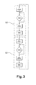
- the figure 3 is a flowchart of said method.
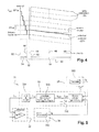
- the figure 4 illustrates the temporal evolution of the output voltages of the switch 36, the output voltage of a selection circuit 221 of a particular digitizing circuit 22 , and a voltage to be converted by this digitizing circuit 22 particular.
- the method comprises two successive phases, namely a first phase 50 for determining the most significant bits of the digital values of the voltages to be digitized, followed by a second phase 60 for determining the least significant bits of said digital values.
- the digitization is carried out on H most significant bits and L least significant bits.
- the number of resistors 344 of the resistive bridge 352 is chosen equal to a power of two, namely 2 H.
- the integer H is chosen to be equal to 3 and the integer L equal to 10, which makes it possible to digitize the voltages delivered by an imaging matrix over 13 bits of effective resolution, a satisfactory fineness in most cases interest.
- the preferential choice of 3 high-order bits makes it possible on the one hand to limit the conversion time 2 L .T C required for the second ramp, which accounts for most of the total conversion time, and to limit on the other hand the number of critical points that make up the passages from one high-weight interval to the next.
- the proposed conversion circuit is designed to meet the need, a very small slope error can produce an error on the last bit, it is therefore necessary to limit the frequency of occurrence of these sensitive conversions, proportional frequency to 2 Hrs .
- the phase 50 for determining the most significant bits begins with the reset of the memories 223 of the digitizing circuits 22, which has the effect of resetting the selection circuits 221, and the closing of the switch 321 of the reference generator 30.
- Switch 321 being closed, the operational amplifier therefore operates as a follower so that the voltages at the nodes of the resistive bridge 342 are constant.
- the switch 36 is also controlled to select the 2 H lowest voltages of the nodes of the bridge 342. These voltages then constitute constant reference voltages, regularly spaced ⁇ V ref between the voltages V min and V max , used for determining the H most significant bits of the digital values of the voltages to be converted.
- Phase 50 then continues, in each digitizing circuit 22, by the sequential selection, at 54, inputs of the selection circuit 221 and the delivery of the selected input to the comparator 222.
- the sequential selection continues as long as the selected input is greater than the voltage to be converted received by the comparator 222 of the corresponding sample-and-hold device 12 .
- the comparator 222 switches, at 56, to its high state.
- the memory 223 then stores in memory the address, that is to say the coding, of the selected input of the selection circuit 221 and transmits a blocking signal thereto.
- the circuit 221 then remains blocked on the address input stored in the memory 223. This address thus constitutes the value of the H most significant bits, increased by one unit, of the digital value of the voltage to be converted.
- the process then continues by the control, at 58, of the switch 36 so that the It selects the highest 2 H voltages at the nodes of the resistive bridge 342. Since the resistors of the resistive bridge 342 are identical, this has the effect of incrementing the constant voltages at the input of the selection circuits 221 by the value ⁇ V ref. , as illustrated in figure 4 .
- the voltage selected by a selection circuit 221 is the reference voltage immediately below the corresponding voltage to be converted and after switching of the switch 36, the voltage selected by the circuit 221 is the voltage of reference immediately superior.
- the second phase 60 of the method aims to determine the value of L least significant bits, using a second comparison implemented by the comparators 222. It is advantageous for the accuracy of the tipping point thereof, that the second comparison is made by approaching the threshold tilt on the same side as during the first comparing the first phase 50. Following the increment of the voltages received by the selection circuits 221, the output voltage of each selection circuit 221 is again greater than the corresponding voltage to be converted. Thus, the comparators 222 all switch to their low state and are therefore ready to change state with the same direction of switching on a crossing of their inputs.
- each memory 223 includes a first zone allocated to the storage of the address of the input of the selection circuit 221 corresponding to the switching of the comparator 222 associated, and a second zone allocated to the storage of the address on which the selection circuit 221 is blocked during the second phase 60.
- the comparator 222 When switching the comparator 222, the The selected address is then copied to the two areas of the memory 223. Once the first phase 50 has ended, the address stored in the first area of each memory 223 is decremented by one unit (and thus forms the pure H bits of weight strong).
- a selection circuit 221 thus selects the reference voltage immediately higher than the corresponding voltage to be converted.
- This variant has the advantage of ensuring a temporal continuity of the voltages conveyed in the bus 42 between the phases 50 and 60, while maintaining the immunity with respect to the "Schmidt trigger” effect and also makes it possible to eliminate the switch 36.
- the second phase 60 for determining the low-order bits then starts after a predetermined time following the switchover of the switch 36, by the opening, at 62, of the switch 323 of the reference generator 30. Simultaneously, the time counter 40 is reset.
- the closing of the switch 323 thus initiates, in each digitizing circuit 22, a decay step 64 of the voltage at the output of the selection circuit 221 in a continuous ramp of constant slope of theoretical value ⁇ ⁇ Vref 2 The . T VS , as shown in the figure 4 .
- the comparator 222 then switches to its high state at 66.
- the memory 223 then stores the value of the time counter 40, this value thus constituting the value of the L least significant bits of the digital value of the voltage to be converted.
- the second phase 60 then ends once the duration 2 L .T C elapsed since the closing of the switch 323, thus ensuring that all low-order bits of the voltages to be converted has been determined.
- the contents of the memories 223 are then, at 68, read and delivered to a communication interface by means of a serial multiplexer.
- the 3 most significant bits pass through a digital subtracter (not shown, for example disposed after the serial multiplexer, or even downstream of the read circuit) to decrement them all by one unit.
- the comparator 222 inverted its output during the formation of the most significant bits while the address of the reference voltage selected at the input had increased by an excess unit. Note that in the proposed variant where the switch 36 is omitted, this subtraction is already performed between the phases 50 and 60, the high-order bits are then directly contained in the first area of the memories 223.
- the second phase 60 then loops on the first phase 50 for a new conversion cycle of new voltages delivered by the sample-and-hold devices 12.
- the address coding of the references by the selector 221 will advantageously be according to what the person skilled in the art calls a "Gray code” rather than by numerical addresses ordered according to a standard binary growth.
- This code is characterized by the variation of a single address bit during the passage of any reference to an adjacent reference, thus avoiding the possibility of inadvertent switchover of the comparator 222 during the discrete scanning of the first digitization phase, according to a technique well known to those skilled in the art.
- the identity of the bridges 34 and 35 is introduced for the sake of clarity up to this point of the exposition, but it will be easily understood that it is advantageous to produce only the identity of the voltages appearing at the equivalent nodes. said bridges. Indeed, it is very simple to produce resistors 354 and Rb X times higher to form the resistive bridge 352 with respect to the resistors 344 and Rb ' forming the resistive bridge 342, which delivers virtually no current to its nodes, so to divide by the same ratio X its consumption.
- the supply transistors 341 will also be duplicated X times in parallel with the architecture of the bridge 35 so as to ensure the identity of behavior of the potential nodes despite the current ratio X between the two bridges. The overall consumption of the analog circuit 30 is thus minimized to the necessary extent.
- a source of inaccuracy of the digital conversion according to the invention can come from the set formed by the voltage genesis circuit 33 and the integrator 32 in charge of the genesis of the voltage ramp.
- the current generating circuit 33 delivers a current strictly equal to VS . ⁇ ⁇ Vref 2
- the . T VS at a given moment and under given operating conditions, that is to say which produces the desired theoretical value ⁇ ⁇ Vref 2
- the . T VS for the slope of the voltage ramp, it is not guaranteed to obtain a ramp which causes the increment ⁇ Vref to decrease during the duration 2 L .T C at another time or when the operating conditions change.
- the theoretical value of the slope assumes the use of a perfect operational amplifier 321 , and a value C of the capacitance 322 exactly calibrated and constant.
- the generator circuit 33 is configured to determine a current I R as a function of the real decay of a voltage of a node of the resistive bridge 342, that is to say as a function of the actual slope of the voltage ramp.
- This loop 70 for adjusting the slope of the voltage ramp used for the determination of the low-order bits.
- This loop 70 comprises the circuit 33, the integrator 32, as well as the resistive bridges 34 and 35.
- the circuit 33 is connected to a node of the resistive bridge 342 to receive the voltage V B thereof, as well as to a set-point circuit delivering a voltage V A equal to the desired value for the voltage V B halfway through. slope during its decay phase, that is to say the value of this voltage at the moment 2 The . T VS 2 after the closing of the switch 323 of the reference generator 30.
- the setpoint circuit advantageously consists of the second resistive bridge 352.
- the resistance of the bridge 352 corresponding to the resistance of the first resistive bridge 342 at the node from which the voltage V B is taken, is formed of two resistors in series of value R 2 and the voltage V A is taken at the intermediate node between these two resistors.
- the current I approx is an approximate current corresponding to a preset of the current I R on a value close to or equal to VS . ⁇ ⁇ Vref 2
- the . T VS and the current I corr is a current correction current I approx to obtain the desired slope.
- control transistors 33122, 33132 are biased in such a way as to operate continuously in the on mode, that is to say with a gate-source voltage V GS substantially above their threshold voltage V t so that the variations of the differential input V B -VA are correctly translated by a differential current I gen, as is detailed below.
- phases 1 The adjustment of the slope of the ramp consists of an alternation of first phases during which the switch 323 is closed (called “phases 1" as shown in FIG. figure 9 which illustrates the evolution of the voltages V A and V B over time), and second phases during which the switch 323 is open during the duration 2 L .T C (called “phase 2" as represented on the figure 9 ).
- the adjustment of the ramp is performed during the digitization of the voltages.
- the selection signal salt is equal to the control signal of the switch 323 and the signal selB is equal to the complement thereof.
- the timing diagram of the salt selection signal is represented at figure 10 .
- the signal salt is set low and the signal selB is set to high.
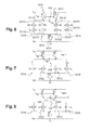
- the transistors 33121, 33131 forming switches of the internal branches 3312, 3313 are then in their off state, and the transistors 33141, 33151 forming switches of the external branches 3312, 3313 are in their on state, as illustrated in FIG. figure 7 which illustrates the state of said transistors by an open circuit or by a short circuit.
- the control transistors 33142, 33152 of the external branches receiving on their gate the same voltage V A , they are therefore balanced so that the same current I goes through them. As a result, no current flows in the direction of the capacitor 332 which thus maintains a constant voltage V CD at its terminals.
- V CD ech constant throughout the second phase that follows.
- the signal salt is set high and the signal selB is set to the low state.
- the transistors 33121, 33131 forming switches of the internal branches 3312, 3313 are then in their conducting state, and the transistors 33141, 33151 forming switches of the external branches 3312, 3313 are in their blocking state, as illustrated in FIG. figure 8 which illustrates the state of said transistors by an open circuit or by a short circuit.
- V CD ech imposes a voltage ramp on the injection node of the resistive bridge 342.
- the voltage V B therefore follows said ramp, as illustrated in FIG. figure 9 by the decreasing portions of it.
- control transistors 33122, 33132 of the internal branches 3312, 3313 respectively receiving on their gate different voltages V A and V B these branches are therefore unbalanced. It thus circulates in the internal branch 3312 controlled by the voltage V A current I - I gen 2 , and in the internal branch 3313 controlled by the voltage V B a current I + I gen 2 .
- the differential pair provides a linear I gen current with respect to the input signal when the relationship 2 V GS - V t > V B - V AT ⁇ max is satisfied, where (V GS -V t ) is the pass-mode bias margin of control MOSs 33122 and 33132 beyond their threshold voltage V t .
- the differential pair is correctly polarized when the relationship V GS - V t > ⁇ ⁇ V ref 2 ⁇ 2 is satisfied.
- slave means the relation between I gen and the differential signal (V B -V A ), this servocontrol being proportional if the detection circuit 331 operates in linear mode.
- a current I gen of sign equal to the sign of the voltage difference V B -V A is thus circulated in the capacitor 332 .
- This current I gen is thus integrated in the capacitor 332 for the duration 2 L .T C that the second phase lasts.
- the voltage V CD keeps the same value at the end of the second phase. Since the voltage V A is chosen equal to the desired value for the mid-slope voltage V B , this means that the voltage V B has exactly decreased by the increment ⁇ V ref during the duration 2 L .T C. Therefore, the current I R is set to the value to obtain this desired decrease.
- the figure 11 represents the time evolution of the voltages V C and V D at the two terminals of the capacitor 332 and the figure 12 , the temporal evolution of the term V CD ech .
- the initial value of the current I R is too low and does not allow a sufficient decrease in the voltage V B (the decrease ⁇ V R of the first second phase is smaller than the increment ⁇ V ref ).
- the voltage V CD no longer varies, as is visible on the figure 11 , as the term V CD ech , as is visible on the figure 12 .
- a stationary state is obtained in a few cycles by natural convergence of the genesis circuit of voltages 33 towards said ideal slope, because of the fractional feedback. cycle to cycle implemented by it.
- Said stationary state corresponds to the stable asymptotic value of the differential voltage V CD taken across the capacitor 332.
- This voltage thus forms an "error signal" which corresponds to the particular value imposing through the voltage source 333 the value particular ramp current I R which produces the balance of the charging and discharging times of the capacitor 332 over the duration 2 L .T C of the ramp.
- the second phase ramp produced at equilibrium by the integrator 32 by integrating the current I R supplied by the circuit 33 produces a voltage path V B from V A + ⁇ V ref / 2 to V A - ⁇ V ref / 2.
- the total ramp voltage excursion is equal to ⁇ V ref , a high-order digitization increment, over the time slot allocated to the second phase, or by definition 2 L .T c . This is the result sought to ensure the accuracy of low-weight scanning.
- the figure 13 is a schematic view of a preferred embodiment of the current source 333.
- the current source 333 comprises two branches 3331 and 3332 between a voltage V DD and ground.
- Each of these branches comprises a p-channel field effect transistor 33311, 33321 whose source is connected to the voltage V DD and whose gate is connected to its drain, an n-channel field effect transistor 33312, 33322 , whose drain is connected to the drain of the transistor 33311, 33321 and a constant current source 33313, 33323 connected between the source of transistor 33312, 33322 and the mass.
- These current sources are sized and biased to provide the current I approx .
- the voltage difference V CD is applied between the gates of the transistors 33312, 33322.
- the gates of the transistors 33321 of the current source 333 and the transistor constituting the current mirror 334 are connected to an armature of a holding capacitor whose other armature is connected to a fixed potential. Said grids are connected together by a switch 3334 controlled by the "salt" signal disposed upstream of said capacitor.
- This arrangement constitutes a sample-and-hold device for the control voltage of the mirror, in other words of the current I res , alternately and equivalent to sampling upstream of the voltage V CD to form the voltage V CD ech proposed above for clarity of presentation. According to this form of circuit, the voltage V CD is not sampled.
- This current source 333 which thus functions as a voltage / current converter, has the advantage of having a very high input impedance, which makes it possible not to degrade the voltage V CD across the capacitor 332.
- the internal loopback of the reference generator 30 makes it possible to ensure the temporal connection of the reference voltages between the various scanning phases, whatever the temperature variations of the converter, and even the technological variations of a converter to the other.
- the distribution accuracy of the resistances according to the circuits 34 and 35 and the identity of the copies of the charging current I ref are sufficient in relation to the target performances of the converter, the operation accuracy of the converter is automatically maintained whatever the Operating temperature.
- the physical constituents of the converter according to the invention opposite characteristics related to technological dispersions.
Landscapes
- Engineering & Computer Science (AREA)
- Theoretical Computer Science (AREA)
- Multimedia (AREA)
- Signal Processing (AREA)
- Analogue/Digital Conversion (AREA)
- Transforming Light Signals Into Electric Signals (AREA)
Applications Claiming Priority (1)
| Application Number | Priority Date | Filing Date | Title |
|---|---|---|---|
| FR1052433A FR2958471B1 (fr) | 2010-03-31 | 2010-03-31 | Procede de conversion analogique/numerique parallele, dispositif mettant en oeuvre un tel procede et detecteur d'imagerie comportant un tel dispositif |
Publications (2)
| Publication Number | Publication Date |
|---|---|
| EP2372917A1 true EP2372917A1 (de) | 2011-10-05 |
| EP2372917B1 EP2372917B1 (de) | 2012-03-21 |
Family
ID=43063690
Family Applications (1)
| Application Number | Title | Priority Date | Filing Date |
|---|---|---|---|
| EP11305327A Not-in-force EP2372917B1 (de) | 2010-03-31 | 2011-03-24 | Gerät zur parallelen Analog-Digital-Wandlung und ein solches Gerät umfassender Bildgebungsdetektor |
Country Status (4)
| Country | Link |
|---|---|
| US (1) | US8658959B2 (de) |
| EP (1) | EP2372917B1 (de) |
| AT (1) | ATE550832T1 (de) |
| FR (1) | FR2958471B1 (de) |
Families Citing this family (4)
| Publication number | Priority date | Publication date | Assignee | Title |
|---|---|---|---|---|
| JP5858695B2 (ja) * | 2011-09-08 | 2016-02-10 | キヤノン株式会社 | 固体撮像装置及び固体撮像装置の駆動方法 |
| US9197225B2 (en) * | 2011-10-05 | 2015-11-24 | International Business Machines Corporation | Control voltage mirror circuit |
| KR20160103302A (ko) * | 2015-02-24 | 2016-09-01 | 에스케이하이닉스 주식회사 | 램프전압 제너레이터 및 그를 포함하는 이미지 센싱 장치 |
| EP3435046B1 (de) * | 2017-07-26 | 2019-12-25 | ams International AG | Optische sensoranordnung und verfahren zur lichterfassung |
Family Cites Families (6)
| Publication number | Priority date | Publication date | Assignee | Title |
|---|---|---|---|---|
| DE3773940D1 (de) * | 1987-12-15 | 1991-11-21 | Itt Ind Gmbh Deutsche | Abtast-halte-stufe und deren anwendung in parallel-a/d-wandlern. |
| US5099239A (en) * | 1989-09-21 | 1992-03-24 | Xerox Corporation | Multi-channel analogue to digital convertor |
| US5283582A (en) * | 1991-12-20 | 1994-02-01 | Texas Instruments Incorporated | Circuitry and method for current input analog to digital conversion |
| US7164379B1 (en) * | 2005-11-30 | 2007-01-16 | General Electric Company | Pipeline analog to digital converter |
| US7336214B2 (en) * | 2005-12-16 | 2008-02-26 | Alexander Krymski | Analog to digital converter circuit with offset reduction and image sensor using the same |
| US7999716B2 (en) * | 2006-10-04 | 2011-08-16 | Nagasaki University, National University Corporation | Analog-digital conversion circuit, timing signal generating circuit, and control device |
-
2010
- 2010-03-31 FR FR1052433A patent/FR2958471B1/fr not_active Expired - Fee Related
-
2011
- 2011-03-24 EP EP11305327A patent/EP2372917B1/de not_active Not-in-force
- 2011-03-24 AT AT11305327T patent/ATE550832T1/de active
- 2011-03-30 US US13/075,856 patent/US8658959B2/en not_active Expired - Fee Related
Non-Patent Citations (4)
| Title |
|---|
| E. MOTTIN ET AL.: "Uncooled amorphous silicon ehancement for 25gm pixel pitch achievement", INFRARED TECHNOLOGY AND APPLICATION XXVIII, SPIE, vol. 4820 |
| MARTIJN F SNOEIJ ET AL: "Multiple-Ramp Column-Parallel ADC Architectures for CMOS Image Sensors", IEEE JOURNAL OF SOLID-STATE CIRCUITS, IEEE SERVICE CENTER, PISCATAWAY, NJ, US, vol. 42, no. 12, 1 December 2007 (2007-12-01), pages 2968 - 2977, XP011197063, ISSN: 0018-9200, DOI: 10.1109/JSSC.2007.908720 * |
| P. GRAY, R. MEYER: "Analysis and design of analog integrated circuits", 9 April 2001, J. WILEY & SONS, pages: 220 |
| SEUNGHYUN LIM ET AL: "A High-Speed CMOS Image Sensor With Column-Parallel Two-Step Single-Slope ADCs", IEEE TRANSACTIONS ON ELECTRON DEVICES, IEEE SERVICE CENTER, PISACATAWAY, NJ, US, vol. 56, no. 3, 1 March 2009 (2009-03-01), pages 393 - 398, XP011252327, ISSN: 0018-9383 * |
Also Published As
| Publication number | Publication date |
|---|---|
| FR2958471A1 (fr) | 2011-10-07 |
| ATE550832T1 (de) | 2012-04-15 |
| US20110240833A1 (en) | 2011-10-06 |
| US8658959B2 (en) | 2014-02-25 |
| EP2372917B1 (de) | 2012-03-21 |
| FR2958471B1 (fr) | 2012-08-24 |
Similar Documents
| Publication | Publication Date | Title |
|---|---|---|
| EP3140906B1 (de) | Vorrichtung mit hohem dynamikumfang zur integration eines elektrischen stroms | |
| CA2760468C (fr) | Systeme et procede de detection de rayonnement infrarouge | |
| EP2307864B1 (de) | Einrichtung und verfahren zum detektieren von infrarotstrahlung durch eine widerstands-bolometermatrix | |
| CA2619564C (fr) | Procede pour numeriser une grandeur analogique, dispositif de numerisation mettant en oeuvre ce procede et detecteur de rayonnements electromagnetiques integrant un tel dispositif | |
| EP2632150B1 (de) | Korrekturverfahren der Abweichung eines Infrarotsensors, der eine Matrix aus bildgebenden Widerstandsbolometern umfasst, und Vorrichtung zur Umsetzung dieses Verfahrens | |
| EP2687020B1 (de) | Bildaufnehmer | |
| EP2770312A1 (de) | Bolometrischer Detektor mit temperaturabhängiger, kontrollierter Polarisation | |
| EP2966454A1 (de) | Verfahren zum Messen eines physikalischen Parameters, und elektronischer Schaltkreis zu dessen Umsetzung | |
| EP3021571B1 (de) | Cmos-bildsensor mit analog-digital-umwandlung vom typ sigma-delta | |
| CA2632505A1 (fr) | Dispositif de detection de rayonnement infrarouge a detecteurs bolometriques | |
| FR2973161A1 (fr) | Capteur d'image a double temps d'integration et selection conditionnelle | |
| FR2943199A1 (fr) | Procede de lecture de signal de capteur d'image et capteur d'image. | |
| EP2372917B1 (de) | Gerät zur parallelen Analog-Digital-Wandlung und ein solches Gerät umfassender Bildgebungsdetektor | |
| EP2015038A1 (de) | Elektronischer Sensor mit integrierter Thermoregulierung | |
| EP3084377B1 (de) | Messschaltung für einen bolometrischen detektor | |
| CA3089379A1 (fr) | Dispositif haute dynamique pour l'integration d'un courant electrique | |
| EP2327160B1 (de) | Analogzähler und ein einen solchen zähler enthaltenden bildgeber | |
| EP4216564B1 (de) | Kalibrierung eines digitalen iwr-pixels eines bildsensors | |
| EP0749234B1 (de) | Halbleiter-Bildsensor mit integrierte Pixelhistogrammumwandlung | |
| WO2024156940A1 (fr) | Calibration d'un pixel numérique iwr d'imageur | |
| FR2574606A1 (fr) | Convertisseur numerique analogique a redistribution de charges capacitives avec autocalibration | |
| EP2579009A1 (de) | System und Verfahren zur Erfassung von Infrarotstrahlung |
Legal Events
| Date | Code | Title | Description |
|---|---|---|---|
| PUAI | Public reference made under article 153(3) epc to a published international application that has entered the european phase |
Free format text: ORIGINAL CODE: 0009012 |
|
| AK | Designated contracting states |
Kind code of ref document: A1 Designated state(s): AL AT BE BG CH CY CZ DE DK EE ES FI FR GB GR HR HU IE IS IT LI LT LU LV MC MK MT NL NO PL PT RO RS SE SI SK SM TR |
|
| AX | Request for extension of the european patent |
Extension state: BA ME |
|
| 17P | Request for examination filed |
Effective date: 20110929 |
|
| GRAP | Despatch of communication of intention to grant a patent |
Free format text: ORIGINAL CODE: EPIDOSNIGR1 |
|
| RIC1 | Information provided on ipc code assigned before grant |
Ipc: H03M 1/56 20060101ALN20111110BHEP Ipc: H03M 1/76 20060101ALN20111110BHEP Ipc: H03M 1/14 20060101AFI20111110BHEP |
|
| RIC1 | Information provided on ipc code assigned before grant |
Ipc: H03M 1/56 20060101ALN20111115BHEP Ipc: H03M 1/14 20060101AFI20111115BHEP Ipc: H03M 1/76 20060101ALN20111115BHEP |
|
| GRAS | Grant fee paid |
Free format text: ORIGINAL CODE: EPIDOSNIGR3 |
|
| GRAA | (expected) grant |
Free format text: ORIGINAL CODE: 0009210 |
|
| AK | Designated contracting states |
Kind code of ref document: B1 Designated state(s): AL AT BE BG CH CY CZ DE DK EE ES FI FR GB GR HR HU IE IS IT LI LT LU LV MC MK MT NL NO PL PT RO RS SE SI SK SM TR |
|
| REG | Reference to a national code |
Ref country code: GB Ref legal event code: FG4D Free format text: NOT ENGLISH |
|
| REG | Reference to a national code |
Ref country code: CH Ref legal event code: EP |
|
| REG | Reference to a national code |
Ref country code: IE Ref legal event code: FG4D Free format text: LANGUAGE OF EP DOCUMENT: FRENCH |
|
| REG | Reference to a national code |
Ref country code: AT Ref legal event code: REF Ref document number: 550832 Country of ref document: AT Kind code of ref document: T Effective date: 20120415 |
|
| REG | Reference to a national code |
Ref country code: DE Ref legal event code: R096 Ref document number: 602011000018 Country of ref document: DE Effective date: 20120516 |
|
| REG | Reference to a national code |
Ref country code: SE Ref legal event code: TRGR |
|
| REG | Reference to a national code |
Ref country code: NL Ref legal event code: VDEP Effective date: 20120321 |
|
| PG25 | Lapsed in a contracting state [announced via postgrant information from national office to epo] |
Ref country code: NO Free format text: LAPSE BECAUSE OF FAILURE TO SUBMIT A TRANSLATION OF THE DESCRIPTION OR TO PAY THE FEE WITHIN THE PRESCRIBED TIME-LIMIT Effective date: 20120621 Ref country code: LT Free format text: LAPSE BECAUSE OF FAILURE TO SUBMIT A TRANSLATION OF THE DESCRIPTION OR TO PAY THE FEE WITHIN THE PRESCRIBED TIME-LIMIT Effective date: 20120321 |
|
| LTIE | Lt: invalidation of european patent or patent extension |
Effective date: 20120321 |
|
| PG25 | Lapsed in a contracting state [announced via postgrant information from national office to epo] |
Ref country code: FI Free format text: LAPSE BECAUSE OF FAILURE TO SUBMIT A TRANSLATION OF THE DESCRIPTION OR TO PAY THE FEE WITHIN THE PRESCRIBED TIME-LIMIT Effective date: 20120321 Ref country code: LV Free format text: LAPSE BECAUSE OF FAILURE TO SUBMIT A TRANSLATION OF THE DESCRIPTION OR TO PAY THE FEE WITHIN THE PRESCRIBED TIME-LIMIT Effective date: 20120321 Ref country code: GR Free format text: LAPSE BECAUSE OF FAILURE TO SUBMIT A TRANSLATION OF THE DESCRIPTION OR TO PAY THE FEE WITHIN THE PRESCRIBED TIME-LIMIT Effective date: 20120622 Ref country code: RS Free format text: LAPSE BECAUSE OF FAILURE TO SUBMIT A TRANSLATION OF THE DESCRIPTION OR TO PAY THE FEE WITHIN THE PRESCRIBED TIME-LIMIT Effective date: 20120321 |
|
| REG | Reference to a national code |
Ref country code: AT Ref legal event code: MK05 Ref document number: 550832 Country of ref document: AT Kind code of ref document: T Effective date: 20120321 |
|
| PG25 | Lapsed in a contracting state [announced via postgrant information from national office to epo] |
Ref country code: CY Free format text: LAPSE BECAUSE OF FAILURE TO SUBMIT A TRANSLATION OF THE DESCRIPTION OR TO PAY THE FEE WITHIN THE PRESCRIBED TIME-LIMIT Effective date: 20120321 |
|
| PG25 | Lapsed in a contracting state [announced via postgrant information from national office to epo] |
Ref country code: MC Free format text: LAPSE BECAUSE OF NON-PAYMENT OF DUE FEES Effective date: 20120331 Ref country code: RO Free format text: LAPSE BECAUSE OF FAILURE TO SUBMIT A TRANSLATION OF THE DESCRIPTION OR TO PAY THE FEE WITHIN THE PRESCRIBED TIME-LIMIT Effective date: 20120321 Ref country code: IS Free format text: LAPSE BECAUSE OF FAILURE TO SUBMIT A TRANSLATION OF THE DESCRIPTION OR TO PAY THE FEE WITHIN THE PRESCRIBED TIME-LIMIT Effective date: 20120721 Ref country code: EE Free format text: LAPSE BECAUSE OF FAILURE TO SUBMIT A TRANSLATION OF THE DESCRIPTION OR TO PAY THE FEE WITHIN THE PRESCRIBED TIME-LIMIT Effective date: 20120321 Ref country code: CZ Free format text: LAPSE BECAUSE OF FAILURE TO SUBMIT A TRANSLATION OF THE DESCRIPTION OR TO PAY THE FEE WITHIN THE PRESCRIBED TIME-LIMIT Effective date: 20120321 Ref country code: PL Free format text: LAPSE BECAUSE OF FAILURE TO SUBMIT A TRANSLATION OF THE DESCRIPTION OR TO PAY THE FEE WITHIN THE PRESCRIBED TIME-LIMIT Effective date: 20120321 Ref country code: SI Free format text: LAPSE BECAUSE OF FAILURE TO SUBMIT A TRANSLATION OF THE DESCRIPTION OR TO PAY THE FEE WITHIN THE PRESCRIBED TIME-LIMIT Effective date: 20120321 |
|
| PG25 | Lapsed in a contracting state [announced via postgrant information from national office to epo] |
Ref country code: PT Free format text: LAPSE BECAUSE OF FAILURE TO SUBMIT A TRANSLATION OF THE DESCRIPTION OR TO PAY THE FEE WITHIN THE PRESCRIBED TIME-LIMIT Effective date: 20120723 Ref country code: SK Free format text: LAPSE BECAUSE OF FAILURE TO SUBMIT A TRANSLATION OF THE DESCRIPTION OR TO PAY THE FEE WITHIN THE PRESCRIBED TIME-LIMIT Effective date: 20120321 |
|
| REG | Reference to a national code |
Ref country code: SE Ref legal event code: EUG |
|
| PLBE | No opposition filed within time limit |
Free format text: ORIGINAL CODE: 0009261 |
|
| STAA | Information on the status of an ep patent application or granted ep patent |
Free format text: STATUS: NO OPPOSITION FILED WITHIN TIME LIMIT |
|
| PG25 | Lapsed in a contracting state [announced via postgrant information from national office to epo] |
Ref country code: DK Free format text: LAPSE BECAUSE OF FAILURE TO SUBMIT A TRANSLATION OF THE DESCRIPTION OR TO PAY THE FEE WITHIN THE PRESCRIBED TIME-LIMIT Effective date: 20120321 Ref country code: AT Free format text: LAPSE BECAUSE OF FAILURE TO SUBMIT A TRANSLATION OF THE DESCRIPTION OR TO PAY THE FEE WITHIN THE PRESCRIBED TIME-LIMIT Effective date: 20120321 Ref country code: NL Free format text: LAPSE BECAUSE OF FAILURE TO SUBMIT A TRANSLATION OF THE DESCRIPTION OR TO PAY THE FEE WITHIN THE PRESCRIBED TIME-LIMIT Effective date: 20120321 |
|
| 26N | No opposition filed |
Effective date: 20130102 |
|
| PG25 | Lapsed in a contracting state [announced via postgrant information from national office to epo] |
Ref country code: SE Free format text: LAPSE BECAUSE OF NON-PAYMENT OF DUE FEES Effective date: 20120325 |
|
| REG | Reference to a national code |
Ref country code: DE Ref legal event code: R097 Ref document number: 602011000018 Country of ref document: DE Effective date: 20130102 |
|
| PG25 | Lapsed in a contracting state [announced via postgrant information from national office to epo] |
Ref country code: HR Free format text: LAPSE BECAUSE OF FAILURE TO SUBMIT A TRANSLATION OF THE DESCRIPTION OR TO PAY THE FEE WITHIN THE PRESCRIBED TIME-LIMIT Effective date: 20121121 |
|
| PG25 | Lapsed in a contracting state [announced via postgrant information from national office to epo] |
Ref country code: BG Free format text: LAPSE BECAUSE OF FAILURE TO SUBMIT A TRANSLATION OF THE DESCRIPTION OR TO PAY THE FEE WITHIN THE PRESCRIBED TIME-LIMIT Effective date: 20120621 |
|
| BERE | Be: lapsed |
Owner name: ULIS Effective date: 20130331 |
|
| PG25 | Lapsed in a contracting state [announced via postgrant information from national office to epo] |
Ref country code: ES Free format text: LAPSE BECAUSE OF FAILURE TO SUBMIT A TRANSLATION OF THE DESCRIPTION OR TO PAY THE FEE WITHIN THE PRESCRIBED TIME-LIMIT Effective date: 20120702 |
|
| PG25 | Lapsed in a contracting state [announced via postgrant information from national office to epo] |
Ref country code: HR Free format text: LAPSE BECAUSE OF FAILURE TO SUBMIT A TRANSLATION OF THE DESCRIPTION OR TO PAY THE FEE WITHIN THE PRESCRIBED TIME-LIMIT Effective date: 20120321 |
|
| REG | Reference to a national code |
Ref country code: IE Ref legal event code: MM4A |
|
| PG25 | Lapsed in a contracting state [announced via postgrant information from national office to epo] |
Ref country code: AL Free format text: LAPSE BECAUSE OF FAILURE TO SUBMIT A TRANSLATION OF THE DESCRIPTION OR TO PAY THE FEE WITHIN THE PRESCRIBED TIME-LIMIT Effective date: 20120321 Ref country code: BE Free format text: LAPSE BECAUSE OF NON-PAYMENT OF DUE FEES Effective date: 20130331 Ref country code: IE Free format text: LAPSE BECAUSE OF NON-PAYMENT OF DUE FEES Effective date: 20130324 |
|
| PG25 | Lapsed in a contracting state [announced via postgrant information from national office to epo] |
Ref country code: TR Free format text: LAPSE BECAUSE OF FAILURE TO SUBMIT A TRANSLATION OF THE DESCRIPTION OR TO PAY THE FEE WITHIN THE PRESCRIBED TIME-LIMIT Effective date: 20120321 |
|
| PG25 | Lapsed in a contracting state [announced via postgrant information from national office to epo] |
Ref country code: HU Free format text: LAPSE BECAUSE OF FAILURE TO SUBMIT A TRANSLATION OF THE DESCRIPTION OR TO PAY THE FEE WITHIN THE PRESCRIBED TIME-LIMIT Effective date: 20110324 Ref country code: MT Free format text: LAPSE BECAUSE OF FAILURE TO SUBMIT A TRANSLATION OF THE DESCRIPTION OR TO PAY THE FEE WITHIN THE PRESCRIBED TIME-LIMIT Effective date: 20120321 |
|
| REG | Reference to a national code |
Ref country code: CH Ref legal event code: PL |
|
| PG25 | Lapsed in a contracting state [announced via postgrant information from national office to epo] |
Ref country code: CH Free format text: LAPSE BECAUSE OF NON-PAYMENT OF DUE FEES Effective date: 20140331 Ref country code: LI Free format text: LAPSE BECAUSE OF NON-PAYMENT OF DUE FEES Effective date: 20140331 |
|
| PGFP | Annual fee paid to national office [announced via postgrant information from national office to epo] |
Ref country code: IT Payment date: 20150325 Year of fee payment: 5 |
|
| PG25 | Lapsed in a contracting state [announced via postgrant information from national office to epo] |
Ref country code: SM Free format text: LAPSE BECAUSE OF FAILURE TO SUBMIT A TRANSLATION OF THE DESCRIPTION OR TO PAY THE FEE WITHIN THE PRESCRIBED TIME-LIMIT Effective date: 20120321 |
|
| PG25 | Lapsed in a contracting state [announced via postgrant information from national office to epo] |
Ref country code: MK Free format text: LAPSE BECAUSE OF FAILURE TO SUBMIT A TRANSLATION OF THE DESCRIPTION OR TO PAY THE FEE WITHIN THE PRESCRIBED TIME-LIMIT Effective date: 20120321 Ref country code: LU Free format text: LAPSE BECAUSE OF NON-PAYMENT OF DUE FEES Effective date: 20120324 |
|
| REG | Reference to a national code |
Ref country code: FR Ref legal event code: PLFP Year of fee payment: 6 |
|
| PG25 | Lapsed in a contracting state [announced via postgrant information from national office to epo] |
Ref country code: IT Free format text: LAPSE BECAUSE OF NON-PAYMENT OF DUE FEES Effective date: 20160324 |
|
| REG | Reference to a national code |
Ref country code: FR Ref legal event code: PLFP Year of fee payment: 7 |
|
| REG | Reference to a national code |
Ref country code: FR Ref legal event code: PLFP Year of fee payment: 8 |
|
| PGFP | Annual fee paid to national office [announced via postgrant information from national office to epo] |
Ref country code: GB Payment date: 20220316 Year of fee payment: 12 Ref country code: DE Payment date: 20220307 Year of fee payment: 12 |
|
| PGFP | Annual fee paid to national office [announced via postgrant information from national office to epo] |
Ref country code: SE Payment date: 20220316 Year of fee payment: 12 Ref country code: FR Payment date: 20220329 Year of fee payment: 12 |
|
| REG | Reference to a national code |
Ref country code: DE Ref legal event code: R119 Ref document number: 602011000018 Country of ref document: DE |
|
| REG | Reference to a national code |
Ref country code: SE Ref legal event code: EUG |
|
| GBPC | Gb: european patent ceased through non-payment of renewal fee |
Effective date: 20230324 |
|
| PG25 | Lapsed in a contracting state [announced via postgrant information from national office to epo] |
Ref country code: GB Free format text: LAPSE BECAUSE OF NON-PAYMENT OF DUE FEES Effective date: 20230324 |
|
| PG25 | Lapsed in a contracting state [announced via postgrant information from national office to epo] |
Ref country code: SE Free format text: LAPSE BECAUSE OF NON-PAYMENT OF DUE FEES Effective date: 20230325 Ref country code: GB Free format text: LAPSE BECAUSE OF NON-PAYMENT OF DUE FEES Effective date: 20230324 Ref country code: FR Free format text: LAPSE BECAUSE OF NON-PAYMENT OF DUE FEES Effective date: 20230331 Ref country code: DE Free format text: LAPSE BECAUSE OF NON-PAYMENT OF DUE FEES Effective date: 20231003 |