EP2372997B1 - Procédé et appareil de formation d'image - Google Patents
Procédé et appareil de formation d'image Download PDFInfo
- Publication number
- EP2372997B1 EP2372997B1 EP11158385.2A EP11158385A EP2372997B1 EP 2372997 B1 EP2372997 B1 EP 2372997B1 EP 11158385 A EP11158385 A EP 11158385A EP 2372997 B1 EP2372997 B1 EP 2372997B1
- Authority
- EP
- European Patent Office
- Prior art keywords
- density
- pixel
- unit
- image data
- pixels
- Prior art date
- Legal status (The legal status is an assumption and is not a legal conclusion. Google has not performed a legal analysis and makes no representation as to the accuracy of the status listed.)
- Not-in-force
Links
- 238000000034 method Methods 0.000 title claims description 105
- 230000008569 process Effects 0.000 claims description 86
- 238000012937 correction Methods 0.000 claims description 17
- 238000010586 diagram Methods 0.000 description 51
- 238000012545 processing Methods 0.000 description 36
- 238000006243 chemical reaction Methods 0.000 description 21
- 238000012546 transfer Methods 0.000 description 21
- 238000007639 printing Methods 0.000 description 17
- 230000006870 function Effects 0.000 description 15
- 230000015572 biosynthetic process Effects 0.000 description 14
- 239000004065 semiconductor Substances 0.000 description 14
- 238000012935 Averaging Methods 0.000 description 13
- 230000003287 optical effect Effects 0.000 description 12
- 230000006866 deterioration Effects 0.000 description 8
- 238000001514 detection method Methods 0.000 description 4
- 230000001360 synchronised effect Effects 0.000 description 4
- 238000005516 engineering process Methods 0.000 description 3
- 230000002093 peripheral effect Effects 0.000 description 3
- 238000003491 array Methods 0.000 description 2
- 238000004140 cleaning Methods 0.000 description 2
- 238000012217 deletion Methods 0.000 description 2
- 230000037430 deletion Effects 0.000 description 2
- 239000002985 plastic film Substances 0.000 description 2
- MCSOAHVAIJXNDN-ZTFGCOKTSA-N ram-322 Chemical compound C1C(=O)CC[C@@]2(O)[C@H]3CC4=CC=C(OC)C(O)=C4[C@]21CCN3C MCSOAHVAIJXNDN-ZTFGCOKTSA-N 0.000 description 2
- 230000004044 response Effects 0.000 description 2
- 230000002411 adverse Effects 0.000 description 1
- XAGFODPZIPBFFR-UHFFFAOYSA-N aluminium Chemical compound [Al] XAGFODPZIPBFFR-UHFFFAOYSA-N 0.000 description 1
- 229910052782 aluminium Inorganic materials 0.000 description 1
- 238000003705 background correction Methods 0.000 description 1
- 230000005540 biological transmission Effects 0.000 description 1
- 238000004891 communication Methods 0.000 description 1
- 230000007547 defect Effects 0.000 description 1
- 238000009792 diffusion process Methods 0.000 description 1
- 230000000694 effects Effects 0.000 description 1
- 229920001971 elastomer Polymers 0.000 description 1
- 230000004907 flux Effects 0.000 description 1
- 230000005484 gravity Effects 0.000 description 1
- 238000003384 imaging method Methods 0.000 description 1
- 230000006872 improvement Effects 0.000 description 1
- 238000003780 insertion Methods 0.000 description 1
- 230000037431 insertion Effects 0.000 description 1
- 239000000463 material Substances 0.000 description 1
- 239000011159 matrix material Substances 0.000 description 1
- 229920006255 plastic film Polymers 0.000 description 1
- 229920002379 silicone rubber Polymers 0.000 description 1
- 230000003068 static effect Effects 0.000 description 1
Images


Classifications
-
- H—ELECTRICITY
- H04—ELECTRIC COMMUNICATION TECHNIQUE
- H04N—PICTORIAL COMMUNICATION, e.g. TELEVISION
- H04N1/00—Scanning, transmission or reproduction of documents or the like, e.g. facsimile transmission; Details thereof
- H04N1/04—Scanning arrangements, i.e. arrangements for the displacement of active reading or reproducing elements relative to the original or reproducing medium, or vice versa
- H04N1/047—Detection, control or error compensation of scanning velocity or position
-
- H—ELECTRICITY
- H04—ELECTRIC COMMUNICATION TECHNIQUE
- H04N—PICTORIAL COMMUNICATION, e.g. TELEVISION
- H04N1/00—Scanning, transmission or reproduction of documents or the like, e.g. facsimile transmission; Details thereof
- H04N1/40—Picture signal circuits
- H04N1/40068—Modification of image resolution, i.e. determining the values of picture elements at new relative positions
Definitions
- the present invention relates to image formation, and more particularly, to an image forming apparatus and an image forming method for forming a latent image with multiple beams.
- the image formation rate of the image forming apparatus per unit time i.e., the number of prints per minute (PPM) increases.
- PPM the number of prints per minute
- an image forming apparatus which performs multi-beam exposure using a vertical cavity surface emitting laser hereinafter, referred to as a "VCSEL"
- VCSEL vertical cavity surface emitting laser
- a time interval between printing an image on the first side of a sheet and printing an image on the second side tends to be shortened.
- some apparatuses perform printing images on the first and second sides within 10 seconds.
- the present invention has been made in view of the above, and an object of the present invention is to provide an image forming apparatus and an image forming method capable of achieving formation of a high-resolution image at a high speed even in duplex printing without causing global image deterioration, and also capable of preventing the appearance of banding.
- US 2008/239336 A1 pertains to an optical scanning device, an optical scanning method, and an image forming apparatus.
- an image forming apparatus includes: an image-data acquiring unit (302) that acquires image data composed of a plurality of pixels; a resolution converting unit (350a, 350b, 350c, 350d, 350e) that converts a resolution of the acquired image data into a higher resolution than the resolution of the image data; a position determining unit (354) that performs a position determining process of determining a position of an additional pixel to be added on the basis of main-scanning directional positions of pixels composing the converted image data and respective shift amounts of the pixels shifted to a sub-scanning direction from the main-scanning directional positions; a density determining unit (355a) that determines a density of the additional pixel on the basis of a density of a pixel located at a position corresponding to the determined position in the acquired image data; a correcting unit (350d) that performs a correction process of adding the additional pixel having the determined density to the determined position; and a scaling unit
- an image forming method comprises: acquiring image data composed of a plurality of pixels; converting a resolution of the acquired image data into a higher resolution than the resolution of the image data; performing a position determining process of determining a position of an additional pixel to be added on the basis of main-scanning directional positions of pixels composing the converted image data and respective shift amounts of the pixels shifted to a sub-scanning direction from the main-scanning directional positions; determining a density of the additional pixel on the basis of a density of a pixel located at a position corresponding to the determined position in the acquired image data; performing a correction process of adding the additional pixel having the determined density to the determined position; and scaling the image data up or down by repeatedly performing the position determining process and the correction process with respect to each of sub-scanning lines of pixels and then repeatedly performing the position determining process and the correction process with respect to each of main-scanning lines of pixels by controlling a position determining unit (354) and a correct
- FIG. 1 is a schematic diagram illustrating a mechanical configuration of an image forming apparatus according to a first embodiment.
- an image forming apparatus 100 mainly includes: an optical device 102 including optical elements such as a VCSEL 200 (see Figs. 2 and 3 ) and a polygon mirror 102a; an image forming unit 112 including photosensitive drums charging devices, developing devices, and the like; and a transfer unit 122 including an intermediate transfer belt and the like.
- the optical device 102 includes the VCSEL 200 as a semiconductor laser.
- light beams emitted from the VCSEL 200 (not shown in Fig. 1 ) are first collected by a first cylindrical lens (not shown), and deflected to a reflection mirrors 102b by the polygon mirror 102a.
- the VCSEL 200 here is a surface-emitting semiconductor laser in which a plurality of light sources (semiconductor lasers) is arranged on the same chip in a lattice pattern.
- Various technologies for an image forming apparatus using such a VCSEL 200 are known; the optical device 102 of the image forming apparatus 100 according to the present embodiment incorporates the VCSEL 200 in a configuration similar to those of the publicly-known technologies.
- Fig. 2 is a configuration diagram of the VCSEL 200 incorporated in the optical device 102 according to the present embodiment.
- the VCSEL 200 according to the present embodiment is, as shown in Fig.
- the VCSEL 200 composed of a semiconductor laser array that a plurality of light sources 1001 (a plurality of semiconductor lasers) is arranged in a lattice pattern.
- the VCSEL 200 is installed so that an array direction of the plurality of light sources 1001 is tilted at a predetermined angle ⁇ to a rotating shaft of the polygon mirror 102a provided as a deflector.
- Fig. 2 vertical arrays of the light sources are denoted by a to c, and lateral arrays are denoted by 1 to 4; for example, the top-left light source 1001 in Fig. 2 is denoted by a1. Since the light sources 1001 are obliquely arranged at a polygon mirror angle ⁇ with respect to a sub-scanning direction, it is assumed that the light source a1 and the light source a2 expose different scanning positions to light, and a pixel (one pixel) is constructed by this two light sources, i.e., in Fig. 2 , one pixel is achieved by two light sources.
- pixels as illustrated on the extreme right in Fig. 2 are formed by the light sources in the drawing.
- a center-to-center distance between adjacent pixels each constructed by two light sources is equivalent to 600 dpi.
- a center-to-center distance between the two light sources constructing one pixel is equivalent to 1200 dpi, and the light-source density is twice as much as the pixel density. Therefore, by changing a light quantity ratio of light sources constructing one pixel, the position of the gravity center of the pixel can be displaced in the sub-scanning direction, and it is possible to achieve high-precision image formation.
- the image forming apparatus 100 includes the post-object type optical device 102 which does not use an f-theta lens.
- the post-object type optical device 102 which does not use an f-theta lens.
- light beams L respectively corresponding to cyan (C), magenta (M), yellow (Y), and black (K) image data are emitted, and reflected by the reflection mirrors 102b, and then again collected by second cylindrical lenses 102c, and after that, photosensitive drums 104a, 106a, 108a, and 110a are exposed to the light beams L, respectively.
- the main scanning direction is defined as a scanning direction of the light beams
- the sub-scanning direction is defined as a direction perpendicular to the main scanning direction.
- Each of the photosensitive drums 104a, 106a, 108a, and 110a includes a photoconductive layer including at least a charge generation layer and a charge transport layer on a conductive drum made of aluminum or the like.
- the photoconductive layers are provided to correspond to the photosensitive drums 104a, 106a, 108a, and 110a, and applied with surface charges by charger units 104b, 106b, 108b, and 110b each including a corotron, a scorotron, or a charging roller, respectively.
- Static charges applied to the photosensitive drums 104a, 106a, 108a, and 110a by the respective charger units 104b, 106b, 108b, and 110b are exposed to the light beams L, and electrostatic latent images are formed.
- the electrostatic latent images formed on the photosensitive drums 104a, 106a, 108a, and 110a are developed by developing units 104c, 106c, 108c, and 110c each including a developing sleeve, a developer supply roller, a control blade, and the like, respectively, and developer images are formed.
- the developer images formed on the photosensitive drums 104a, 106a, 108a, and 110a are transferred onto an intermediate transfer belt 114, which moves in a direction of an arrow A in accordance with rotation of conveying rollers 114a, 114b, and 114c, in a superimposed manner.
- the superimposed C, M, Y, and K developer images (hereinafter, referred to as a "multicolor developer image") transferred onto the intermediate transfer belt 114 are conveyed to a secondary transfer unit in accordance with the movement of the intermediate transfer belt 114.
- the secondary transfer unit includes a secondary transfer belt 118 and conveying rollers 118a and 118b.
- the secondary transfer belt 118 moves in a direction of an arrow B in accordance with rotation of the conveying rollers 118a and 118b.
- An image receiving medium 124 such as high-quality paper or a plastic sheet, is fed from an image-receiving-media containing unit 128, such as a paper cassette, to the secondary transfer unit by a conveying roller 126.
- the secondary transfer unit applies a secondary bias to the intermediate transfer belt 114, whereby the multicolor developer image on the intermediate transfer belt 114 is transferred onto the image receiving medium 124 attracted and held on the secondary transfer belt 118.
- the image receiving medium 124 is supplied to a fixing unit 120 in accordance with the movement of the secondary transfer belt 118.
- the fixing unit 120 includes a fixing member 130, such as a fixing roller made of silicon rubber or fluorine-contained rubber, and applies heat and pressure to the image receiving medium 124 and the multicolor developer image, and outputs the image receiving medium 124 as a printed material 132 to outside the image forming apparatus 100.
- a cleaning unit 116 including a cleaning blade removes transfer residual developers from the intermediate transfer belt 114 to make ready for a next image forming process.
- Fig. 3 is a schematic perspective view illustrating a case where the optical device 102 including the VCSEL 200 exposes the photosensitive drum 104a to a light beam L.
- the light beam L emitted from the VCSEL 200 is collected by a first cylindrical lens 202 used to shape a light beam flux, and goes through a reflection mirror 204 and an imaging lens 206, and then is deflected by the polygon mirror 102a.
- the polygon mirror 102a is driven to rotate by, for example, a spindle motor which spins several thousand times to tens of thousands times per minute.
- the light beam L is again shaped by the second cylindrical lens 102c, and the photosensitive drum 104a is exposed to the light beam L.
- a reflection mirror 208 is arranged.
- the reflection mirror 208 reflects the light beam L to a synchronization detection device 210 including a photodiode and the like before the scanning in the sub-scanning direction is started.
- the synchronization detection device 210 When detecting the light beam, the synchronization detection device 210 generates a synchronization signal to start sub-scanning, and synchronizes a process, such as a process of generating a drive control signal to the VCSEL 200.
- the VCSEL 200 is driven by a pulse signal sent from a GAVD 310 to be described later, and as described later, the position on the photosensitive drum 104a corresponding to a predetermined image bit of image data is exposed to a light beam L emitted from the VCSEL 200, and an electrostatic latent image is formed on the photosensitive drum 104a.
- Fig. 4 is a schematic functional block diagram of a control unit 300 of the image forming apparatus 100.
- the control unit 300 includes a scanner unit 302, a printer unit 308, and a main control unit 330.
- the scanner unit 302 functions as a means for reading an image, and includes a VPU 304 and an IPU 306.
- the VPU 304 converts an analog signal read by a scanner into a digital signal, and performs a black offset correction, a shading correction, and a pixel location correction.
- the IPU 306 performs image processing mainly for converting the acquired image in the RGB color system into digital image data in the CMYK color system.
- the read image acquired by the scanner unit 302 is output as digital data to the printer unit 308.
- the printer unit 308 includes the GAVD 310, an LD driver 312, and the VCSEL 200.
- the GAVD 310 functions as a control means for performing the drive control of the VCSEL 200.
- the LD driver 312 supplies a current for driving a semiconductor laser element to the semiconductor laser element in response to a drive control signal generated by the GAVD 310.
- the VCSEL 200 mounts thereon two-dimensionally-arranged semiconductor laser elements.
- the GAVD 310 executes a resolution increasing process on image data transmitted from the scanner unit 302 by dividing pixel data in a size corresponding to the spatial size of the semiconductor laser elements of the VCSEL 200.
- the scanner unit 302 and the printer unit 308 are connected to the main control unit 330 via a system bus 316, and image reading and image formation are controlled by a command from the main control unit 330.
- the main control unit 330 includes a central processing unit (CPU) 320 and a RAM 322.
- the RAM 322 provides a processing space used by the CPU 320 to process image data. Any CPUs that have been known can be used as the CPU 320; for example, a CISC (Complex Instruction Set Computer), such as the PENTIUM (registered trademark) series and a PENTIUM-compatible CPU, a RISC (Reduced Instruction Set Computer), such as the MIPS, and the like can be used.
- CISC Complex Instruction Set Computer
- PENTIUM registered trademark
- a RISC Reduced Instruction Set Computer
- the CPU 320 receives an instruction from a user via an interface 328, and calls a program module for executing a process corresponding to the instruction to execute the process, such as copy, facsimile, scan, or image storage.
- the main control unit 330 further includes a ROM 324, and stores default setting data of the CPU 320, control data, a program, and the like in the ROM 324 so that the CPU 320 can use them.
- An image storage 326 is configured as a fixed or removable memory device, such as a hard disk device, an SD card, and a USB memory, and stores therein image data acquired by the image forming apparatus 100 so that the image data can be used for various processes instructed by a user.
- the CPU 320 executes the main-scanning direction control and the sub-scanning position control of an image receiving medium, such as high-quality paper or a plastic film.
- the CPU 320 outputs a start signal to the GAVD 310.
- an IPU 306 starts a scanning process.
- the GAVD 310 receives image data stored in a buffer memory or the like, and processes the received image data, and then outputs the processed image data to the LD driver 312.
- the LD driver 312 When receiving the image data from the GAVD 310, the LD driver 312 generates a drive control signal of the VCSEL 200. After that, the LD driver 312 sends the drive control signal to the VCSEL 200, thereby lighting up the VCSEL 200.
- the LD driver 312 drives the semiconductor laser elements by the use of the PWM control or the like.
- the VCSEL 200 described in the present embodiment includes eight channels of semiconductor laser elements; however, the number of channels of the VCSEL 200 is not limited to eight.
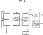
- Fig. 5 is a detailed functional block diagram of the GAVD 310.
- the GAVD 310 receives a synchronization signal, and includes a memory 340 such as a FIFO buffer for storing and memorizing image data sent from the IPU 306, and passes the image data sent from the IPU 306 to an image processing unit 342 in a first-in first-out method.
- the image processing unit 342 reads out the image data from the memory 340, and executes a resolution conversion of the image data, assignment of the channel of the semiconductor laser element, and a process of adding/deleting an image bit (i.e., a correction pixel for scaling the image data up or down) (i.e., a correction process of the image data).
- the position on the photosensitive drum 104a exposed to a light beam corresponding to the image data is defined by a main-scanning line address value defining a line address value in the main-scanning direction and a sub-scanning line address value defining a line address value in the sub-scanning direction.
- address coordinates are defined as a set of address values to which a specific image bit is given when image data is specified by a main-scanning line address value (an R address value) and a sub-scanning line address value (an F address value).
- these address values are determined by an address generating unit 354.
- address coordinates are set by each row of pixels aligned in each main-scanning line and each sub-scanning line.
- An image path selector 358 to be described below performs a correction process, such as insertion of an image bit, with respect to a pixel located at an address of coordinates specified by an R address value and an F address value which is determined by the address generating unit 354 to be described below (i.e., at a pixel position) by each row of pixels.
- An output-data control unit 344 converts output data, which is a write signal corresponding to the image data generated by the image processing unit 342, into a time-series drive pulse on the basis of the F address value and the sub-scanning speed, and generates a synchronization control signal for giving a synchronization signal to a synchronization detection device 210, and adds the generated synchronization control signal to the drive pulse.
- the generated drive control signal is transmitted to the LD driver 312, and the VCSEL (not shown) is driven.
- the output-data control unit 344 receives a synchronization signal from the synchronization detection device 210, and synchronizes the transmission of the drive control signal to the LD driver 312.
- processes of the memory 340, the image processing unit 342, and the output-data control unit 344 are synchronized with an operation clock from a PLL 346.
- Fig. 6 is a functional block diagram of an image processing unit 342a according to the first embodiment.
- the image processing unit 342a mainly includes a resolution converting unit 350a and a sub-scanning scaling control unit 352a.
- the resolution converting unit 350a creates divided pixels by dividing a unit pixel of image data acquired from the memory 340 in the corresponding size and number of channels of the VCSEL 200. After that, the resolution converting unit 350a assigns the channels of the laser elements, which emit laser beams to respective pixels, to the divided pixels. Furthermore, in the case of increasing the resolution, the resolution converting unit 350a selects a 2n-fold density process (n is a positive integer) or a 2n-line process, and determines the assignment of the channel of the laser element to be driven. In this case, the resolution converting unit 350a determines synchronous writing of a 1200-dpi input image for a plurality of lines by the eight channels of the VCSEL at an output resolution of 4800 dpi.
- a resolution converting unit 350 converts input image data (hereinafter, referred to as "input data”) into image data of a higher resolution (hereinafter, referred to as an "output resolution") than a resolution (hereinafter, referred to as an "input resolution”) of an input image.
- Fig. 7 is a schematic diagram for explaining the resolution increasing process performed by the resolution converting unit 350. As shown in Fig. 7 , the resolution converting unit 350 converts input data D0[1:0] illustrated on the left side of the diagram into output data Dc0[3:0] to Dc3[3:0] illustrated on the right side of the diagram depending on the density of the input data.
- the resolution converting unit 350 converts the input data DO[1:0] having an input resolution of 1200 dpi into the output data Dc0[3:0] to Dc3[3:0] having an output resolution of 4800 dpi.
- the resolution converting unit 350 processes other input data D1[1:0] to D5[1:0] in the same manner as the input data D0[1:0].
- the resolution converting unit 350 converts the input data D1[1:0] into output data Dc4[3:0] to Dc7[3:0].
- the resolution converting unit 350a determines data causing the VCSEL 200 to be turned on from the input data. For example, when D0[1:0] to D5[1:0] for 6 lines are input data, it is assumed that D2[1:0] and D3[1:0] are attention lines and others are reference lines. When shift operation in a sub-scanning scaling process to be described below is not made, the resolution converting unit 350a sets the data causing the VCSEL 200 to be turned on as data of an attention line; on the other hand, when shift operation in the sub-scanning scaling process is made, the resolution converting unit 350a sets the data causing the VCSEL 200 to be turned on as reference image data.
- the sub-scanning scaling control unit 352a mainly includes the address generating unit 354, a density determining unit 355a, a memory 356, and the image path selector 358.
- the address generating unit 354 determines an adding address value indicating an address of image data to which an image bit is added in an image enlarging process.
- the address generating unit 354 corresponds to a position determining unit of the present invention.
- the memory 356 stores therein a shift amount of an image bit, and counts and holds the number of scale command signals used in a scaling process performed by the image path selector 358 to be described below. Furthermore, the memory 356 holds density data.
- the density data here means data including the pixel density of a reference image, a shift amount of an additional pixel in converted image data, and the density of the additional pixel in an associated manner.
- Fig. 8 is a diagram showing an example of the density data according to the first embodiment.
- the density data includes the pixel density of a reference image, a shift amount of an additional pixel in the sub-scanning direction in converted image data (hereinafter, referred to as a "phase"), and the density of the additional pixel in an associated manner.
- An address of a pixel of the reference image corresponding to an adding address value may be associated with the density data in advance, or may be obtained by calculation.
- the density of an additional pixel which is preliminarily determined in the density data shown in Fig. 8 may be determined as the same density as a corresponding pixel by the resolution conversion shown in Fig. 7 , or may be determined as a different density.
- % denotes a remainder.
- a phase is taken into consideration in determination of the density of an additional pixel; alternatively, the density of an additional pixel may be determined on the basis of only the density of a pixel of a reference image corresponding to an adding address value without taking a phase into consideration.
- the density determining unit 355a determines the density of an additional pixel from an adding address value and the density of a pixel of a reference image corresponding to the adding address value.
- the reference image here means image data having an input resolution before being converted by the sub-scanning scaling control unit 352a.
- the additional pixel here means a pixel added to an address indicated by the adding address value.
- the density determining unit 355a specifies the density of a pixel of a reference image corresponding to an adding address value determined by the address generating unit 354 from the density data shown in Fig. 8 , and obtains the density of a corresponding additional pixel.
- the density determining unit 355a may specify the densities of pixels of an reference image corresponding to an adding address value and around the adding address value (hereinafter, referred to as "surrounding pixels").
- the surrounding pixels may be only pixels adjacent to the adding address value, or may be two to three rows of pixels around adding address values of both an R address value and an F address value.
- the density determining unit 355a determines the density of an additional pixel from an adding address value and the density of a pixel of a reference image corresponding to the adding address value. For example, the density determining unit 355a determines the same density as a pixel of a reference image corresponding to an adding address value as the density of an additional pixel.
- the image path selector 358 scales the image data converted by the resolution converting unit 350a up or down. Specifically, the image path selector 358 obtains the determined adding address value (the F address value and the R address value) from the address generating unit 354. Furthermore, the image path selector 358 determines whether an address value subject to the process includes the adding address value. For example, when the address value subject to the process includes the adding address value, the image path selector 358 generates a scale command signal, such as an add flag, and passes the generated scale command signal to the memory 356.
- a scale command signal such as an add flag
- the image path selector 358 determines that the address value subject to the process includes the adding address value, i.e., when the scale command signal is set, the image path selector 358 adds an additional pixel having the density determined by the density determining unit 355a to the adding address value, and shifts the subsequent image data by 1 bit.
- the image path selector 358 determines that the address value subject to the process does not include the adding address value, i.e., when the scale command signal is not set, the image path selector 358 selects input data from the resolution converting unit 350a on the basis of a shift amount obtained from the memory 356, and outputs the selected input data.
- the eight-channel VCSEL 200 when the eight-channel VCSEL 200 is used as a semiconductor laser, signals each indicating the position where an image bit is to be added or deleted and signals each indicating a shift amount are assigned to the eight channels (ch0 to ch7), respectively, and are used to drive the VCSEL 200.
- an appropriate operating unit of the image processing unit 342 may be configured as a dedicated module for performing the addition/deletion of an image bit, or a part of another module may be configured to perform the addition/deletion of an image bit.
- the reason why it is configured to count the number of scale command signals is, when an image bit is shifted, to specify, for example, a position to which an image bit is first added in the second scanning after an image bit is added in the first scanning.
- FIGs. 9A and 9B are explanatory diagrams illustrating the operation of the image path selector 358.
- Attention data 602 shown in Figs. 9A and 9B indicates a bit value for one pixel, and the 1-pixel data is represented in sub-coordinates for the eight channels.
- the attention data 602 is bit data assigned to a specific main-scanning coordinate position.
- the attention data 602 and scaling data for specifying a unit of shift for sub-scanning scaling are constantly read out from the memory 340 on the preceding stage, and after the same process is performed on all the lines, the data is input to the resolution converting unit 350.
- Fig. 9B shows a case where a white pixel is added to a sub-coordinate 1 of the attention data 602 in the first scanning (A).
- a signal indicating addition of an image bit is set with an address value corresponding to ch1, and bit data of ch1 is replaced so as to correspond to a white pixel and set as data in ch1 of output data 606.
- a count value of 1 corresponding to the addition to ch1 is registered in the memory 356.
- Data of ch2 to ch7 is each shifted to a sub-coordinate value by a channel shift amount of -1 as a value of a sub-coordinate of the output data 606.
- the image path selector 358 allocates bit data of the channel of the attention data corresponding to the channel shift amount of -1 to ch2 to ch7 of the output data 606, thereby adding an image bit.
- An image bit corresponding to white is added to the attention data in the output data 606, and the output data 606 is used as a write signal.
- the output-data control unit 344 converts the write signal in time series and generates a drive pulse for driving the VCSEL 200, and image formation is performed. The process described above is performed on a main-scanning basis, and data on the next pixel in the main-scanning direction is sequentially read out from the memory 340, and image formation in the main-scanning direction is performed.
- the sub-coordinate values of ch1 to ch7 of the output data 606 are shifted due to the addition of the white pixel; so in the second scanning (B), as shown in Fig. 9B , even when a white pixel is not added, sub-coordinate values are shifted by -1, ch0 to ch7 of the output data 606 output the sub-coordinate values 7 to 14 respectively; furthermore, in the third scanning (C), when a white pixel is added in the same manner as in the first scanning, as shown in Fig. 9B , sub-coordinate values are shifted by -2.
- Fig. 10 is a flowchart showing the procedure of the additional-pixel-density determining process performed by the image processing unit 342a.
- the resolution converting unit 350 acquires image data from the memory 340 as input data (Step S1).
- the resolution converting unit 350 converts the resolution of the acquired input data (Step S2).
- the resolution converting unit 350 converts the resolution of the acquired input data into an output resolution higher than the input resolution before the conversion.
- the address generating unit 354 sets an R address value (Step S3).
- the address generating unit 354 calculates an F address value from the R address value, and determines the F address value (Step S4). For example, the address generating unit 354 calculates an F address value using the R address value by a scaling method used in the image processing unit 342.
- a density determining unit 355 determines the density of an additional pixel added to the F address value from a reference image corresponding to the determined F address value (Step S5).
- the image path selector 358 scales the image data up by adding an additional pixel having the density determined by the density determining unit 355 to the F address (Step S6).
- the image path selector 358 reads out bit data corresponding to the F address value to be processed, and transfers the bit data to the output-data control unit 344 (Step S7).
- the output-data control unit 344 generates a timing pulse signal corresponding to the position of the pixel, and sends the timing pulse signal to the LD driver 312 to drive the semiconductor laser element.
- the image path selector 358 determines whether the transfer of image data in the range of a default F address assigned 1200 dpi is completed by comparing the F address or receiving an end character bit (Step S8).
- the address generating unit 354 sets the next R address value (Step S9).
- the image path selector 358 determines whether the scanning of a main-scanning range is completed (Step S10).
- the image path selector 358 determines that the scanning of the range in the main-scanning direction is not completed (NO at Step S10), return to Step S4, the processes at Steps S4 to S10 are repeated.
- Step S8 when the image path selector 358 determines that the scanning of the sub-scanning range is not completed (NO at Step S8), return to Step S4, the processes at Steps S4 to S8 are repeated until the scanning of the range of the F address value is completed.
- Step S10 when the image path selector 358 determines that the scanning of the address range to be eventually processed is completed (YES at Step S10), the process is terminated.
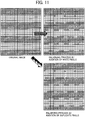
- Fig. 11 is a diagram showing an example of original image data scanned by the scanner unit 302, image data enlarged by a conventional scaling process, and image data enlarged by a scaling process according to the present embodiment.
- the densities of additional pixels "a" are uniformly set as a white pixel, and the original image data is enlarged by adding white pixels to the original image data. Therefore, in the conventional scaling process, for example, when a white pixel is added to a black line, banding may appear on the image due to a decrease in the density.
- the lower section of Fig. 11 shows image data enlarged by the scaling process according to the present embodiment. As shown in Fig.
- the densities of additional pixels "a" are determined on the basis of the densities of pixels corresponding to respective adding address values, and the additional pixels are added.
- an additional black pixel is added into black pixels
- an additional halftone pixel is added into halftone pixels
- an additional white pixel is added into white data; therefore, banding becomes less prominent.
- a high-quality image on which banding is barely prominent is obtained as compared with the image data enlarged by the conventional scaling process.
- the density of an additional pixel is determined on the basis of the density of a pixel at an adding address value; therefore, it is possible to achieve formation of a high-resolution image at high speed even in duplex printing without causing global image deterioration and also possible to prevent the appearance of banding.
- the density determining unit 355a determines the density of an additional pixel on the basis of the density of a pixel at an adding address value or the densities of pixels at an adding address value and around the adding address value.
- the density of an additional pixel is determined on the basis of an average value of the densities of pixels at an adding address value and around the adding address value.
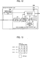
- Fig. 12 is a functional block diagram of an image processing unit 342b according to the second embodiment.
- the image processing unit 342b mainly includes a resolution converting unit 350b and a sub-scanning scaling control unit 352b.
- the sub-scanning scaling control unit 352b mainly includes the address generating unit 354, a density determining unit 355b, an averaging unit 357, a memory 356, and the image path selector 358.
- the functions and configurations of the density determining unit 355b and the averaging unit 357 are explained here.
- the other units other than the density determining unit 355b and the averaging unit 357 have the same configuration and function as those in the first embodiment.
- the averaging unit 357 acquires input data (a reference image) from the memory 340, and calculates an average value of the densities of a pixel to be converted and pixels around the pixel. The averaging unit 357 performs this average-value calculating process with respect to all the pixels.
- the averaging unit 357 acquires more input data than the input data acquired by the resolution converting unit 350a in the first embodiment.
- the averaging unit 357 acquires data of extra 1 or more lines on both the sub-scanning front-end side and the sub-scanning back-end side additionally.
- the averaging unit 357 acquires input data D6[1:0] and D7[1:0] in addition to the input data shown in Fig. 7 .
- the input data D0 and D7 is acquired as reference data.
- input data acquired by the resolution converting unit 350 is the same data D1 to D6 as shown in Fig. 7 .
- the averaging unit 357 obtains the densities of a pixel to be converted and pixels around the pixel (hereinafter, referred to as "surrounding pixels") from a reference image, and calculates an average value of the densities.
- the surrounding pixels here may be only pixels adjacent to an adding address value, or may be two to three rows of pixels around adding address values of both an R address value and an F address value.
- Fig. 13 is an explanatory diagram of operation of the averaging unit 357.
- the averaging unit 357 averages the densities of the pixels 1 to 9.
- the densities that correspond to the pixels 1 to 9 are denoted by densities 1 to densities 9, respectively.
- the density determining unit 355b obtains the average values from the averaging unit 357, and determines a target average value out of the average values obtained from the address generating unit 354 on the basis of the adding address value as the density of an additional pixel.
- An additional-pixel-density determining process is performed by the image processing unit 342b configured as described above.
- a procedure of the additional-pixel-density determining process according to the second embodiment is the same as that is in the first embodiment.
- the density of an additional pixel is determined on the basis of the densities of pixels at an adding address value and around the adding address value; therefore, it is possible to achieve formation of a high-resolution image at high speed even in duplex printing without causing global image deterioration and also possible to prevent the appearance of banding.
- the density of an additional pixel is determined on the basis of the density of a pixel of a reference image corresponding to an adding address value.
- a pixel located at an adding address value is converted into a predetermined code, and the density of an additional pixel is determined on the basis of the code.
- Fig. 14 is a block diagram illustrating a functional configuration of an image processing unit 342c according to the third embodiment.
- the image processing unit 342c mainly includes a resolution converting unit 350c and a sub-scanning scaling control unit 352c.
- the sub-scanning scaling control unit 352c mainly includes a density determining unit 355c, the address generating unit 354, the memory 356, and the image path selector 358.
- the function and configuration of the density determining unit 355c are explained here.
- the other units other than the density determining unit 355c have the same function and configuration as those in the first embodiment.
- the density determining unit 355c mainly includes a code generating unit 355x and a density generating unit 355y.
- the code generating unit 355x converts image data into code data corresponding to a predetermined code.
- Fig. 15 is a diagram showing an example of a pattern used in generation of a code by the code generating unit 355x.
- Fig. 15 shows three examples 1 to 3.
- the center pixel of a 3x3 matrix is an attention pixel, and is a target pixel of which the code is to be output.
- the code is output with reference to the attention pixel and eight surrounding pixels around the attention pixel.
- the predetermined patterns may be preliminarily determined in the hardware configuration, or may be arbitrarily set.
- the density generating unit 355y determines the density of an additional pixel on the basis of the code converted by the code generating unit 355x and density data held in a memory 356.
- Fig. 16 is a diagram showing an example of the density data according to the third embodiment.
- the density data includes a code, a phase, and the density of an additional pixel in an associated manner.
- the density generating unit 355y outputs 4'b1110 as the density of an additional pixel.
- the density generating unit 355y outputs 4'b0000 as the density of an additional pixel.
- the density of an additional pixel in the density data may be preliminarily determined as the hardware configuration, or may be arbitrarily set.
- An additional-pixel-density determining process is performed by the image processing unit 342c configured as described above. Incidentally, a procedure of the additional-pixel-density determining process is the same as that is in the first embodiment.
- the density of an additional pixel is determined on the basis of the densities of pixels at an adding address value and around the adding address value; therefore, it is possible to achieve formation of a high-resolution image at high speed even in duplex printing without causing global image deterioration and also possible to prevent the appearance of banding.
- the resolution converting unit 350 performs a conversion on the basis of an attention pixel of which the resolution is to be converted.
- the resolution converting unit 350 converts the attention pixel so that black dots of the attention pixel are shifted toward a higher-density pixel out of pixels around the attention pixel.
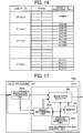
- Fig. 17 is a block diagram illustrating a functional configuration of an image processing unit 342d according to the fourth embodiment.
- the image processing unit 342d mainly includes a resolution converting unit 350d and a sub-scanning scaling control unit 352d.
- the sub-scanning scaling control unit 352d mainly includes a density determining unit 355d, the address generating unit 354, the memory 356, and the image path selector 358.
- the functions and configurations of the resolution converting unit 350d and the density determining unit 355d are explained here.
- the other units other than the resolution converting unit 350d and the density determining unit 355d have the same function and configuration as those in the first embodiment.
- the resolution converting unit 350d creates divided pixels by dividing a unit pixel of image data acquired from the memory 340 in the corresponding size and number of channels of the VCSEL 200. After that, the resolution converting unit 350d assigns the channels of the laser elements, which emit laser beams to respective pixels, to the divided pixels. Furthermore, in the case of increasing the resolution, the resolution converting unit 350d selects a 2n-fold density process (n is a positive integer) or a 2n-line process, and determines the assignment of the channel of the laser element to be driven. In this case, the resolution converting unit 350d determines synchronous writing of a 1200-dpi input image for a plurality of lines by the eight channels of the VCSEL at an output resolution of 4800 dpi.
- the resolution converting unit 350d converts input data into image data of an output resolution higher than an input resolution.
- an attention pixel is a halftone pixel indicating the density between those of a white pixel and a black pixel
- the resolution converting unit 350d converts the attention pixel so that black dots of the attention pixel are shifted toward a higher-density pixel out of the pixels around the attention pixel.
- the resolution converting unit 350d passes shift information indicating a shift direction to the memory 356 and the density determining unit 355d as a signal phs[3:0].
- the memory 356 can hold the signal phs[3:0] received from the resolution converting unit 350d to be associated with density data.
- Fig. 18 is an explanatory diagram showing an example of the shift information.
- the resolution converting unit 350d obtains an attention pixel and pixels around the attention pixel.
- pixels adjacent to the attention pixel are obtained as pixels around the attention pixel; however, the pixels around the attention pixel are not limited to the adjacent pixels, and may be any other pixels as long as the pixels are located in the vicinity of the attention pixel.
- Conditions for judgment of the shift direction include judgment of lateral shift on the basis of pixels located on the left and right sides of the attention pixel and judgment of longitudinal shift on the basis of pixels located on the upper and lower sides of the attention pixel.
- the judgment of lateral shift is made as follows:
- Fig. 19 is an explanatory diagram illustrating a shift conversion performed by the resolution converting unit 350d.
- 2'b00 denotes a white pixel
- 2'b01 and 2'b10 denote halftone pixels
- 2'b11 denotes a black pixel.
- the resolution converting unit 350d converts the halftone pixels 2'b01 and 2'b10 as shown in Fig. 19 in accordance with a result of the shift judgment.
- a mode of conversion depending on the shift judgment may be configured to be fixed by hardware, or may be arbitrarily set by software.
- the density determining unit 355d obtains a signal phs[3:0] from the resolution converting unit 350d, and determines the density of an additional pixel on the basis of the signal phs[3:0] and a phase value. For example, the density determining unit 355d determines the density of an additional pixel on the basis of density data.
- Fig. 20 is a diagram showing an example of the density data according to the fourth embodiment. As shown in Fig. 20 , in the halftone pixel 2'b01 shown in Fig. 19 , a signal phs[3:0] and a phase value are associated with the density of an additional pixel. Furthermore, as shown in Fig.
- An additional-pixel-density determining process is performed by the image processing unit 342d configured as described above.
- a procedure of the additional-pixel-density determining process performed by the image processing unit 342d is the same as that is in the first embodiment.
- the density of an additional pixel is determined on the basis of the densities of pixels at an adding address value and around the adding address value; therefore, it is possible to achieve formation of a high-resolution image at high speed even in duplex printing without causing global image deterioration and also possible to prevent the appearance of banding.
- the resolution converting unit 350d converts a halftone pixel by a shift process.
- a resolution converting unit 350e converts a halftone pixel on the basis of dither information.
- Fig. 21 is a block diagram illustrating a functional configuration of an image processing unit 342e according to the fifth embodiment.
- the image processing unit 342e mainly includes the resolution converting unit 350e and a sub-scanning scaling control unit 352e.
- the sub-scanning scaling control unit 352e mainly includes a density determining unit 355e, the address generating unit 354, the memory 356, and the image path selector 358.
- the functions and configurations of the resolution converting unit 350e and the density determining unit 355e are explained here.
- the other units other than the resolution converting unit 350e and the density determining unit 355e have the same function and configuration as those in the first embodiment.
- the resolution converting unit 350e acquires image data and dither information on dithering performed on the image data from the memory 340.
- the resolution converting unit 350e creates divided pixels by dividing a unit pixel of the acquired image data in the corresponding size and number of channels of the VCSEL 200. After that, the resolution converting unit 350e assigns the channels of the laser elements, which emit laser beams to respective pixels, to the divided pixels. Furthermore, in the case of increasing the resolution, the resolution converting unit 350e selects a 2n-fold density process (n is a positive integer) or a 2n-line process, and determines the assignment of the channel of the laser element to be driven. In this case, the resolution converting unit 350e determines synchronous writing of a 1200-dpi input image for a plurality of lines by the eight channels of the VCSEL at an output resolution of 4800 dpi.
- the resolution converting unit 350e converts input data into image data of an output resolution higher than an input resolution.
- the resolution converting unit 350e performs a conversion on the basis of the dither information. For example, dither information for each color plate is set in advance. This set value may be changed by software or an application on a PC.
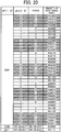
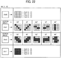
- Fig. 22 is an explanatory diagram showing an example of designation of pixel arrangement based on dither information.
- the dither information includes a screen angle, and a set value depending on the screen angle is preliminarily determined as shown in Fig. 22 .
- the resolution converting unit 350e converts the pixel into the arrangement as shown in Fig. 22 .
- dither information is taken into consideration in the resolution conversion of a halftone pixel only; dither information is not taken into consideration in the resolution conversion of a white pixel 2'b00 and a black pixel 2'b11.
- the density determining unit 355e determines the density of an additional pixel on the basis of dither information and the density of a pixel of a reference image corresponding to an adding address value. With respect to a halftone pixel, the density determining unit 355e acquires dither information from the memory 340, and determines the density of an additional pixel on the basis of image data, the dither information, and an adding address value obtained from the address generating unit 354. Furthermore, with respect to a pixel other than a halftone pixel, i.e., a white pixel and a black pixel, the density determining unit 355e determines the density of a pixel at an adding address value as the density of an additional pixel without taking dither information into consideration.
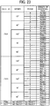
- Fig. 23 is a diagram showing an example of density data according to the fifth embodiment.
- the density data includes dither information, a phase, and the density of an additional pixel in an associated manner.
- the density determining unit 355e determines 4'b4100 as the density of an additional pixel.
- the density determining unit 355e does not take dither information and a phase into consideration.
- the resolution converting unit 350e can convert the density of a halftone pixel into a longitudinal-based density.
- the conversion into the longitudinal-based density means to arrange black dots of a halftone pixel, which is an attention pixel, to be aligned in the sub-scanning direction.
- Fig. 24 is an explanatory diagram showing an example of the conversion into the longitudinal-based density. As shown in Fig.
- the resolution converting unit 350e arranges respective black dots of halftone pixels 2'b01 and 2'b10 to be aligned longitudinally, i.e., in the sub-scanning direction.
- the densities of longitudinally-arranged pixels Dc0[3:0] to Dc3[3:0] can be either all the same data or different data from one another. However, in the case of different data, a difference between the data is preferably as small as possible to avoid banding.
- the resolution converting unit 350e may perform the shift process in the conversion into the longitudinal-based density.
- the density determining unit 355e determines the density of an additional pixel on the basis of the data converted into the longitudinal-based density by the resolution converting unit 350e and a phase.
- the density determining unit 355e can determine the density of an additional pixel directly from the data converted into the longitudinal-based density without taking a phase into consideration.
- the density of each pixel is determined as the density of an additional pixel regardless of phase.
- the density determining unit 355e can determine the density of the additional pixel without taking a phase of the adding position into consideration, so the circuit size can be reduced.
- the resolution converting unit 350e converts the density of a halftone pixel into the lateral-based density, i.e., converts a halftone pixel so that black dots of the halftone pixel are aligned in the main-scanning direction as shown in Fig. 26 , for example, when Dc2[3:0] is deleted, the density varies greatly. Consequently, the resolution converting unit 350e converts the density of a halftone pixel into the longitudinal-based density, and this can make banding less prominent than in the case of the conversion into the lateral-based density.
- An additional-pixel-density determining process is performed by the image processing unit 342e configured as described above.
- a procedure of the additional-pixel-density determining process performed by the image processing unit 342e is the same as that is in the first embodiment.
- the density of an additional pixel is determined on the basis of the densities of pixels at an adding address value and around the adding address value; therefore, it is possible to achieve formation of a high-resolution image at high speed even in duplex printing without causing global image deterioration and also possible to prevent the appearance of banding.
- the density of an additional pixel is determined on the basis of dither information; therefore, it is possible to reduce the adverse effects on not only a line screen but also a dithered image.
- the conversion is made on the basis of the longitudinal-based density; therefore, it is possible to simplify the circuit configuration and reduce the circuit size.
- Fig. 27 is a block diagram illustrating a hardware configuration of the image forming apparatus 100.
- the image forming apparatus 100 (hereinafter, referred to as the "MFP 100") includes a controller 10 and an engine unit 60.
- the controller 10 and the engine unit 60 are connected by a PCI (Peripheral Component Interface) bus.
- the controller 10 is a controller which controls the entire MFP 100 and controls drawing, communications, and the input from an operating unit (not shown).
- the engine unit 60 is a printer engine which can be connected to the PCI bus, etc.
- the engine unit 60 is a black-and-white plotter, a 1-drum color plotter, a 4-drum color plotter, a scanner, a facsimile unit, or the like.
- the engine unit 60 includes an image processing section for performing error diffusion, gamma conversion, or the like on an image in addition to the socalled engine section, such as a plotter.
- the controller 10 includes a CPU 11, a North Bridge (NB) 13, a system memory (MEM-P) 12, a South Bridge (SB) 14, a local memory (MEM-C) 17, an ASIC (Application Specific Integrated Circuit) 16, and a hard disk drive (HDD) 18.
- the NB 13 and the ASIC 16 are connected by an AGP (Accelerated Graphics Port) bus 15.
- the MEM-P 12 includes a ROM (Read Only Memory) 12a and a RAM (Random Access Memory) 12b.
- the CPU 11 controls the entire MFP 100, and has a chipset composed of the NB 13, the MEM-P 12, and the SB 14.
- the CPU 11 is connected to other devices via the chipset.
- the NB 13 is a bridge for connecting the CPU 11 to the MEM-P 12, the SB 14, and the AGP bus 15, and includes a memory controller for controlling read/write with respect to the MEM-P 12 and the like, a PCI master, and an AGP target.
- the MEM-P 12 is a system memory used as a memory for storing a program or data, a memory for unpacking the program or data, a memory for drawing by a printer, and the like, and is composed of the ROM 12a and the RAM 12b.
- the ROM 12a is a read only memory used as a memory for storing a program or data.
- the RAM 12b is a read-write memory used as a memory for unpacking the program or data, a memory for drawing by a printer, and the like.
- the SB 14 is a bridge for connecting the NB 13 to a PCI device and a peripheral device.
- the SB 14 is connected to the NB 13 via the PCI bus, and, for example, a network interface (I/F) is connected to the PCI bus.
- a network interface (I/F) unit and the like are connected to the PCI bus.
- the ASIC 16 is an image processing IC (Integrated Circuit) including hardware components for image processing.
- the ASIC 16 serves as a bridge for connecting the AGP bus 15, the PCI bus, the HDD 18, and the MEM-C 17.
- the ASIC 16 is composed of a PCI target, an AGP master, an arbiter (ARB) which is the core of the ASIC 16, a memory controller for controlling the MEM-C 17, a plurality of DMACs (Direct Memory Access Controllers) for performing rotation of image data or the like by a hardware logic, and a PCI unit for performing data transfer between the controller 10 and the engine unit 60 via the PCI bus.
- AGP master an arbiter
- ARB arbiter
- DMACs Direct Memory Access Controllers
- An FCU (Facsimile Control Unit) 30, a USB (Universal Serial Bus) 40, and an IEEE 1394 (the Institute of Electrical and Electronics Engineers 1394) interface 50 are connected to the ASIC 16 via the PCI bus.
- An operation display unit 20 is directly connected to the ASIC 16.
- the MEM-C 17 is a local memory used as a copy image buffer and a code buffer.
- the HDD 18 is a storage for storing therein image data, a program, font data, and a form.
- the AGP bus 15 is a bus interface for a graphic accelerator card proposed to speed up a graphics operation, and accelerates the graphic accelerator card by directly accessing the MEM-P 12 at high throughput.
Landscapes
- Engineering & Computer Science (AREA)
- Multimedia (AREA)
- Signal Processing (AREA)
- Editing Of Facsimile Originals (AREA)
- Laser Beam Printer (AREA)
- Control Or Security For Electrophotography (AREA)
- Color Electrophotography (AREA)
- Image Processing (AREA)
Claims (9)
- Appareil de formation d'image (100) comprenant :une unité d'acquisition de données d'image (302) conçue pour acquérir des données d'image composées d'une pluralité de pixels ;une unité de conversion de résolution (350a, 350b, 350c, 350d, 350e) conçue pour convertir une résolution des données d'image acquises en une résolution plus élevée que la résolution des données d'image ;une unité de détermination de position (354) conçue pour réaliser un processus de détermination de valeur d'adresse complémentaire consistant à déterminer une valeur d'adresse complémentaire d'un pixel complémentaire devant être ajouté en fonction d'adresses de direction de balayage principal de pixels composant les données d'image converties et d'adresses de direction de balayage secondaire calculées en fonction des adresses de direction de balayage principal ;une unité de détermination de densité (350a, 350b, 350c, 350d, 350e) conçue pour déterminer une densité prédéterminée en tant que densité du pixel complémentaire en fonction d'une densité d'un pixel situé à une position correspondant à la valeur d'adresse complémentaire déterminée dans les données d'image acquises et une quantité de décalage du pixel décalé vers la direction de balayage secondaire, ladite quantité de décalage étant déterminée en fonction de l'adresse de direction de balayage secondaire ;une unité de correction (350d) conçue pour réaliser un processus de correction consistant à ajouter le pixel complémentaire ayant la densité déterminée à la position déterminée ; etune unité de mise à l'échelle conçue pour commander l'unité de détermination de position (354) et l'unité de correction (350d) de manière à ajuster vers le haut ou vers le bas les données d'image en amenant l'unité de détermination de position (354) et l'unité de correction (350d) à réaliser de manière répétée le processus de détermination de valeur d'adresse complémentaire et le processus de correction par rapport à chacune des lignes de balayage secondaire de pixels et puis pour réaliser de manière répétée le processus de détermination de valeur d'adresse complémentaire et le processus de correction par rapport à chacune des lignes de balayage principal de pixels.
- Appareil de formation d'image (100) selon la revendication 1, dans lequel l'unité de détermination de densité (350a, 350b, 350c, 350d, 350e) détermine la densité du pixel complémentaire en fonction de densités de pixels situés à la position correspondant à la position déterminée et autour de la position dans les données d'image acquises.
- Appareil de formation d'image (100) selon la revendication 2, dans lequel l'unité de détermination de densité (350a, 350b, 350c, 350d, 350e) calcule une valeur moyenne des densités des pixels situés à la position correspondant à la position déterminée et autour de la position déterminée dans les données d'image acquises et détermine la valeur moyenne calculée en tant que densité du pixel complémentaire.
- Appareil de formation d'image (100) selon la revendication 2, comprenant en outre :une unité de stockage (356) qui stocke à l'intérieur une pluralité de motifs prédéterminés associés à des valeurs de densité,l'unité de détermination de densité (350a, 350b, 350c, 350d, 350e) comprenant une unité d'obtention de motif qui permet d'obtenir un motif des pixels situés à la position correspondant à la position déterminée et autour de la position déterminée dans les données d'image acquises, etl'unité de détermination de densité (350a, 350b, 350c, 350d, 350e) vérifiant si le motif obtenu correspond à l'un quelconque des motifs stockés dans l'unité de stockage (356) et permettant d'obtenir une valeur de densité associée à un motif correspondant au motif obtenu à partir de l'unité de stockage (356) si le motif obtenu correspond à l'un quelconque des motifs, et puis déterminant la valeur de densité obtenue en tant que densité du pixel complémentaire.
- Appareil de formation d'image (100) selon la revendication 4, dans lequel
l'unité de détermination de densité comprend en outre une unité de réception d'entrée qui reçoit l'entrée de la valeur de densité et le motif,
l'unité de stockage (356) stockant la valeur de densité et le motif dont l'entrée est reçue d'une manière associée. - Appareil de formation d'image (100) selon la revendication 1, dans lequel
par rapport aux pixels en demi-teinte sur les pixels composant les données d'image acquises, l'unité de conversion de résolution convertit en outre le pixel en demi-teinte de manière que les points noirs du pixel en demi-teinte convertis sont décalés vers un pixel de densité élevée sur une pluralité de pixels autour du pixel en demi-teinte, et
l'unité de détermination de densité (350a, 350b, 350c, 350d, 350e) permet d'obtenir des informations de décalage indiquant une direction de décalage du pixel en demi-teinte depuis l'unité de conversion de résolution, et détermine la densité du pixel complémentaire en fonction des informations de décalage et la densité du pixel situé à la position correspondant à la position déterminée. - Appareil de formation d'image (100) selon la revendication 1, dans lequel
l'unité d'acquisition de données d'image (302) acquiert en outre des informations de nuance des données d'image,
par rapport au pixel en demi-teinte sur les pixels composant les données d'image, l'unité de conversion de résolution convertit en outre la résolution en fonction des informations de nuance acquises, et
par rapport au pixel en demi-teinte, l'unité de détermination de densité (350a, 350b, 350c, 350d, 350e) détermine la densité du pixel complémentaire en fonction des informations de nuance et la densité du pixel situé à la position correspondant à la position déterminée. - Appareil de formation d'image (100) selon la revendication 1, dans lequel par rapport au pixel en demi-teinte sur les pixels composant les données d'image acquises, l'unité de conversion de résolution convertit le pixel en demi-teinte de manière que des points noirs du pixel en demi-teinte converti sont agencés pour être alignés dans la direction de balayage secondaire.
- Procédé de formation d'image comprenant :l'acquisition de données d'image composées d'une pluralité de pixels ;la conversion d'une résolution des données d'image acquises en une résolution plus élevée que la résolution des données d'image ;la réalisation d'un processus de détermination de valeur d'adresse complémentaire consistant à déterminer une valeur d'adresse complémentaire d'un pixel complémentaire devant être ajouté en fonction d'adresses de direction de balayage principal de pixels composant les données d'image converties et d'adresses de direction de balayage secondaire calculées en fonction des adresses de direction de balayage principal ;la détermination d'une densité prédéterminée en tant que densité du pixel complémentaire en fonction d'une densité d'un pixel situé à une position correspondant à la valeur d'adresse complémentaire déterminée dans les données d'image acquises et une quantité de décalage du pixel décalé vers la direction de balayage secondaire, ladite quantité de décalage étant déterminée en fonction de l'adresse de direction de balayage secondaire ;la réalisation d'un procédé de correction consistant à ajouter le pixel complémentaire ayant la densité déterminée à la valeur d'adresse complémentaire déterminée ; etl'ajustement vers le haut ou vers le bas des données d'image en réalisant de manière répétée le processus de détermination de valeur d'adresse complémentaire et le processus de correction par rapport à chacune des lignes de balayage secondaire de pixels et puis en réalisant de manière répétée le processus de détermination de valeur d'adresse complémentaire et le processus de correction par rapport à chacune des lignes de balayage principal de pixels en commandant une unité de détermination de position (354) et une unité de correction (350d).
Applications Claiming Priority (1)
| Application Number | Priority Date | Filing Date | Title |
|---|---|---|---|
| JP2010061678A JP5477087B2 (ja) | 2010-03-17 | 2010-03-17 | 画像形成装置および画像形成方法 |
Publications (2)
| Publication Number | Publication Date |
|---|---|
| EP2372997A1 EP2372997A1 (fr) | 2011-10-05 |
| EP2372997B1 true EP2372997B1 (fr) | 2017-11-29 |
Family
ID=43880962
Family Applications (1)
| Application Number | Title | Priority Date | Filing Date |
|---|---|---|---|
| EP11158385.2A Not-in-force EP2372997B1 (fr) | 2010-03-17 | 2011-03-16 | Procédé et appareil de formation d'image |
Country Status (3)
| Country | Link |
|---|---|
| US (2) | US8630015B2 (fr) |
| EP (1) | EP2372997B1 (fr) |
| JP (1) | JP5477087B2 (fr) |
Families Citing this family (5)
| Publication number | Priority date | Publication date | Assignee | Title |
|---|---|---|---|---|
| JP5569067B2 (ja) | 2010-03-17 | 2014-08-13 | 株式会社リコー | 画像形成装置および画像形成方法 |
| JP6277579B2 (ja) | 2012-03-23 | 2018-02-14 | 株式会社リコー | 画像形成装置 |
| JP6172506B2 (ja) * | 2013-05-02 | 2017-08-02 | 株式会社リコー | 画像形成装置及び画像形成方法 |
| JP6171547B2 (ja) * | 2013-05-10 | 2017-08-02 | 株式会社リコー | 画像形成装置、画像形成方法および印刷物の製造方法 |
| JP6269464B2 (ja) * | 2014-12-15 | 2018-01-31 | 京セラドキュメントソリューションズ株式会社 | 画像形成装置、画像形成方法 |
Family Cites Families (16)
| Publication number | Priority date | Publication date | Assignee | Title |
|---|---|---|---|---|
| DE68927970T2 (de) | 1988-09-08 | 1997-10-09 | Canon Kk | Punktbilddatenausgabegerät |
| US5608853A (en) * | 1995-01-19 | 1997-03-04 | Microsoft Corporation | System and method for graphics scaling and localized color enhancement |
| JPH11120341A (ja) * | 1997-10-09 | 1999-04-30 | Ricoh Co Ltd | ディジタル画像形成装置 |
| JP3826666B2 (ja) * | 2000-04-18 | 2006-09-27 | 富士ゼロックス株式会社 | 画像形成装置及び方法 |
| US7738688B2 (en) | 2000-05-03 | 2010-06-15 | Aperio Technologies, Inc. | System and method for viewing virtual slides |
| JP4395743B2 (ja) * | 2004-08-19 | 2010-01-13 | 富士ゼロックス株式会社 | 画像形成装置及び位置ずれ補正方法 |
| JP4865310B2 (ja) | 2005-11-30 | 2012-02-01 | 株式会社リコー | 補正用パターン形成方法及びカラー画像形成装置 |
| JP5017910B2 (ja) * | 2006-04-06 | 2012-09-05 | 富士ゼロックス株式会社 | 画像形成装置 |
| JP4329802B2 (ja) | 2006-10-04 | 2009-09-09 | コニカミノルタビジネステクノロジーズ株式会社 | 画像処理装置及び画像処理方法 |
| US7995251B2 (en) * | 2007-03-30 | 2011-08-09 | Ricoh Company, Limited | Optical scanning device, optical scanning method, and image forming apparatus |
| JP4861253B2 (ja) | 2007-06-12 | 2012-01-25 | 株式会社リコー | 画像処理装置、画像形成装置、プログラムおよび記録媒体 |
| JP4509149B2 (ja) * | 2007-08-03 | 2010-07-21 | キヤノン株式会社 | 画像処理装置及び画像形成装置 |
| EP2040129B1 (fr) | 2007-09-11 | 2018-01-10 | Ricoh Company, Ltd. | Procédé et appareil pour la formation d'images et produit de programme informatique |
| JP5407216B2 (ja) * | 2007-09-11 | 2014-02-05 | 株式会社リコー | 画像形成装置、画像形成方法、画像形成プログラム及び記録媒体 |
| JP5564806B2 (ja) | 2009-03-11 | 2014-08-06 | 株式会社リコー | 画像形成装置、画像形成方法、画像形成プログラム及び記録媒体 |
| JP5569067B2 (ja) | 2010-03-17 | 2014-08-13 | 株式会社リコー | 画像形成装置および画像形成方法 |
-
2010
- 2010-03-17 JP JP2010061678A patent/JP5477087B2/ja not_active Expired - Fee Related
-
2011
- 2011-03-11 US US13/045,850 patent/US8630015B2/en not_active Expired - Fee Related
- 2011-03-16 EP EP11158385.2A patent/EP2372997B1/fr not_active Not-in-force
-
2013
- 2013-12-06 US US14/098,660 patent/US8837016B2/en active Active
Non-Patent Citations (1)
| Title |
|---|
| None * |
Also Published As
| Publication number | Publication date |
|---|---|
| JP2011197158A (ja) | 2011-10-06 |
| JP5477087B2 (ja) | 2014-04-23 |
| US8630015B2 (en) | 2014-01-14 |
| EP2372997A1 (fr) | 2011-10-05 |
| US20110228287A1 (en) | 2011-09-22 |
| US8837016B2 (en) | 2014-09-16 |
| US20140085689A1 (en) | 2014-03-27 |
Similar Documents
| Publication | Publication Date | Title |
|---|---|---|
| US9241089B2 (en) | Image forming apparatus and method for scaling image data by a correction pixel | |
| JP5564806B2 (ja) | 画像形成装置、画像形成方法、画像形成プログラム及び記録媒体 | |
| JP5761279B2 (ja) | 画像形成装置、画像形成方法、画像形成プログラム及び記録媒体 | |
| US8837016B2 (en) | Image forming apparatus and image forming method for adding an additional pixel to image data | |
| JP4045822B2 (ja) | 画像形成装置 | |
| US8817323B2 (en) | Image forming apparatus, image forming method, and computer program product | |
| US8064094B2 (en) | Method and apparatus for performing image size adjustment | |
| US8446641B2 (en) | Image processing apparatus and image processing method | |
| JP2010094982A (ja) | 画像形成装置および画像形成方法 | |
| JP5229168B2 (ja) | 画像処理装置、画像処理方法、及び、画像形成装置 | |
| JP5672349B2 (ja) | 画像形成装置および画像形成方法 | |
| JP5633616B2 (ja) | 画像形成装置および画像形成方法 | |
| JP5402654B2 (ja) | 画像処理装置、画像処理方法、プログラムおよび記録媒体 | |
| JP5660187B2 (ja) | 画像形成装置、画像形成方法、画像形成プログラム及び記録媒体 | |
| JP5614194B2 (ja) | 画像形成装置、画像形成方法、プログラムおよび記録媒体 | |
| JP2022110975A (ja) | 画像形成装置 |
Legal Events
| Date | Code | Title | Description |
|---|---|---|---|
| PUAI | Public reference made under article 153(3) epc to a published international application that has entered the european phase |
Free format text: ORIGINAL CODE: 0009012 |
|
| 17P | Request for examination filed |
Effective date: 20110316 |
|
| AK | Designated contracting states |
Kind code of ref document: A1 Designated state(s): AL AT BE BG CH CY CZ DE DK EE ES FI FR GB GR HR HU IE IS IT LI LT LU LV MC MK MT NL NO PL PT RO RS SE SI SK SM TR |
|
| AX | Request for extension of the european patent |
Extension state: BA ME |
|
| 17Q | First examination report despatched |
Effective date: 20130703 |
|
| GRAP | Despatch of communication of intention to grant a patent |
Free format text: ORIGINAL CODE: EPIDOSNIGR1 |
|
| INTG | Intention to grant announced |
Effective date: 20170623 |
|
| GRAS | Grant fee paid |
Free format text: ORIGINAL CODE: EPIDOSNIGR3 |
|
| GRAA | (expected) grant |
Free format text: ORIGINAL CODE: 0009210 |
|
| AK | Designated contracting states |
Kind code of ref document: B1 Designated state(s): AL AT BE BG CH CY CZ DE DK EE ES FI FR GB GR HR HU IE IS IT LI LT LU LV MC MK MT NL NO PL PT RO RS SE SI SK SM TR |
|
| REG | Reference to a national code |
Ref country code: CH Ref legal event code: EP |
|
| REG | Reference to a national code |
Ref country code: AT Ref legal event code: REF Ref document number: 951355 Country of ref document: AT Kind code of ref document: T Effective date: 20171215 |
|
| REG | Reference to a national code |
Ref country code: IE Ref legal event code: FG4D |
|
| REG | Reference to a national code |
Ref country code: DE Ref legal event code: R096 Ref document number: 602011043714 Country of ref document: DE |
|
| REG | Reference to a national code |
Ref country code: FR Ref legal event code: PLFP Year of fee payment: 8 |
|
| REG | Reference to a national code |
Ref country code: NL Ref legal event code: MP Effective date: 20171129 |
|
| REG | Reference to a national code |
Ref country code: LT Ref legal event code: MG4D |
|
| REG | Reference to a national code |
Ref country code: AT Ref legal event code: MK05 Ref document number: 951355 Country of ref document: AT Kind code of ref document: T Effective date: 20171129 |
|
| PG25 | Lapsed in a contracting state [announced via postgrant information from national office to epo] |
Ref country code: SE Free format text: LAPSE BECAUSE OF FAILURE TO SUBMIT A TRANSLATION OF THE DESCRIPTION OR TO PAY THE FEE WITHIN THE PRESCRIBED TIME-LIMIT Effective date: 20171129 Ref country code: NO Free format text: LAPSE BECAUSE OF FAILURE TO SUBMIT A TRANSLATION OF THE DESCRIPTION OR TO PAY THE FEE WITHIN THE PRESCRIBED TIME-LIMIT Effective date: 20180228 Ref country code: ES Free format text: LAPSE BECAUSE OF FAILURE TO SUBMIT A TRANSLATION OF THE DESCRIPTION OR TO PAY THE FEE WITHIN THE PRESCRIBED TIME-LIMIT Effective date: 20171129 Ref country code: LT Free format text: LAPSE BECAUSE OF FAILURE TO SUBMIT A TRANSLATION OF THE DESCRIPTION OR TO PAY THE FEE WITHIN THE PRESCRIBED TIME-LIMIT Effective date: 20171129 Ref country code: FI Free format text: LAPSE BECAUSE OF FAILURE TO SUBMIT A TRANSLATION OF THE DESCRIPTION OR TO PAY THE FEE WITHIN THE PRESCRIBED TIME-LIMIT Effective date: 20171129 |
|
| PG25 | Lapsed in a contracting state [announced via postgrant information from national office to epo] |
Ref country code: BG Free format text: LAPSE BECAUSE OF FAILURE TO SUBMIT A TRANSLATION OF THE DESCRIPTION OR TO PAY THE FEE WITHIN THE PRESCRIBED TIME-LIMIT Effective date: 20180228 Ref country code: RS Free format text: LAPSE BECAUSE OF FAILURE TO SUBMIT A TRANSLATION OF THE DESCRIPTION OR TO PAY THE FEE WITHIN THE PRESCRIBED TIME-LIMIT Effective date: 20171129 Ref country code: AT Free format text: LAPSE BECAUSE OF FAILURE TO SUBMIT A TRANSLATION OF THE DESCRIPTION OR TO PAY THE FEE WITHIN THE PRESCRIBED TIME-LIMIT Effective date: 20171129 Ref country code: LV Free format text: LAPSE BECAUSE OF FAILURE TO SUBMIT A TRANSLATION OF THE DESCRIPTION OR TO PAY THE FEE WITHIN THE PRESCRIBED TIME-LIMIT Effective date: 20171129 Ref country code: HR Free format text: LAPSE BECAUSE OF FAILURE TO SUBMIT A TRANSLATION OF THE DESCRIPTION OR TO PAY THE FEE WITHIN THE PRESCRIBED TIME-LIMIT Effective date: 20171129 Ref country code: GR Free format text: LAPSE BECAUSE OF FAILURE TO SUBMIT A TRANSLATION OF THE DESCRIPTION OR TO PAY THE FEE WITHIN THE PRESCRIBED TIME-LIMIT Effective date: 20180301 |
|
| PG25 | Lapsed in a contracting state [announced via postgrant information from national office to epo] |
Ref country code: NL Free format text: LAPSE BECAUSE OF FAILURE TO SUBMIT A TRANSLATION OF THE DESCRIPTION OR TO PAY THE FEE WITHIN THE PRESCRIBED TIME-LIMIT Effective date: 20171129 |
|
| PG25 | Lapsed in a contracting state [announced via postgrant information from national office to epo] |
Ref country code: CZ Free format text: LAPSE BECAUSE OF FAILURE TO SUBMIT A TRANSLATION OF THE DESCRIPTION OR TO PAY THE FEE WITHIN THE PRESCRIBED TIME-LIMIT Effective date: 20171129 Ref country code: SK Free format text: LAPSE BECAUSE OF FAILURE TO SUBMIT A TRANSLATION OF THE DESCRIPTION OR TO PAY THE FEE WITHIN THE PRESCRIBED TIME-LIMIT Effective date: 20171129 Ref country code: CY Free format text: LAPSE BECAUSE OF FAILURE TO SUBMIT A TRANSLATION OF THE DESCRIPTION OR TO PAY THE FEE WITHIN THE PRESCRIBED TIME-LIMIT Effective date: 20171129 Ref country code: EE Free format text: LAPSE BECAUSE OF FAILURE TO SUBMIT A TRANSLATION OF THE DESCRIPTION OR TO PAY THE FEE WITHIN THE PRESCRIBED TIME-LIMIT Effective date: 20171129 Ref country code: DK Free format text: LAPSE BECAUSE OF FAILURE TO SUBMIT A TRANSLATION OF THE DESCRIPTION OR TO PAY THE FEE WITHIN THE PRESCRIBED TIME-LIMIT Effective date: 20171129 |
|
| REG | Reference to a national code |
Ref country code: DE Ref legal event code: R097 Ref document number: 602011043714 Country of ref document: DE |
|
| PG25 | Lapsed in a contracting state [announced via postgrant information from national office to epo] |
Ref country code: RO Free format text: LAPSE BECAUSE OF FAILURE TO SUBMIT A TRANSLATION OF THE DESCRIPTION OR TO PAY THE FEE WITHIN THE PRESCRIBED TIME-LIMIT Effective date: 20171129 Ref country code: PL Free format text: LAPSE BECAUSE OF FAILURE TO SUBMIT A TRANSLATION OF THE DESCRIPTION OR TO PAY THE FEE WITHIN THE PRESCRIBED TIME-LIMIT Effective date: 20171129 Ref country code: SM Free format text: LAPSE BECAUSE OF FAILURE TO SUBMIT A TRANSLATION OF THE DESCRIPTION OR TO PAY THE FEE WITHIN THE PRESCRIBED TIME-LIMIT Effective date: 20171129 Ref country code: IT Free format text: LAPSE BECAUSE OF FAILURE TO SUBMIT A TRANSLATION OF THE DESCRIPTION OR TO PAY THE FEE WITHIN THE PRESCRIBED TIME-LIMIT Effective date: 20171129 |
|
| PLBE | No opposition filed within time limit |
Free format text: ORIGINAL CODE: 0009261 |
|
| STAA | Information on the status of an ep patent application or granted ep patent |
Free format text: STATUS: NO OPPOSITION FILED WITHIN TIME LIMIT |
|
| REG | Reference to a national code |
Ref country code: CH Ref legal event code: PL |
|
| 26N | No opposition filed |
Effective date: 20180830 |
|
| PG25 | Lapsed in a contracting state [announced via postgrant information from national office to epo] |
Ref country code: SI Free format text: LAPSE BECAUSE OF FAILURE TO SUBMIT A TRANSLATION OF THE DESCRIPTION OR TO PAY THE FEE WITHIN THE PRESCRIBED TIME-LIMIT Effective date: 20171129 Ref country code: MC Free format text: LAPSE BECAUSE OF FAILURE TO SUBMIT A TRANSLATION OF THE DESCRIPTION OR TO PAY THE FEE WITHIN THE PRESCRIBED TIME-LIMIT Effective date: 20171129 |
|
| REG | Reference to a national code |
Ref country code: BE Ref legal event code: MM Effective date: 20180331 |
|
| REG | Reference to a national code |
Ref country code: IE Ref legal event code: MM4A |
|
| PG25 | Lapsed in a contracting state [announced via postgrant information from national office to epo] |
Ref country code: LU Free format text: LAPSE BECAUSE OF NON-PAYMENT OF DUE FEES Effective date: 20180316 |
|
| PG25 | Lapsed in a contracting state [announced via postgrant information from national office to epo] |
Ref country code: IE Free format text: LAPSE BECAUSE OF NON-PAYMENT OF DUE FEES Effective date: 20180316 |
|
| PG25 | Lapsed in a contracting state [announced via postgrant information from national office to epo] |
Ref country code: LI Free format text: LAPSE BECAUSE OF NON-PAYMENT OF DUE FEES Effective date: 20180331 Ref country code: BE Free format text: LAPSE BECAUSE OF NON-PAYMENT OF DUE FEES Effective date: 20180331 Ref country code: CH Free format text: LAPSE BECAUSE OF NON-PAYMENT OF DUE FEES Effective date: 20180331 |
|
| PG25 | Lapsed in a contracting state [announced via postgrant information from national office to epo] |
Ref country code: MT Free format text: LAPSE BECAUSE OF NON-PAYMENT OF DUE FEES Effective date: 20180316 |
|
| PG25 | Lapsed in a contracting state [announced via postgrant information from national office to epo] |
Ref country code: TR Free format text: LAPSE BECAUSE OF FAILURE TO SUBMIT A TRANSLATION OF THE DESCRIPTION OR TO PAY THE FEE WITHIN THE PRESCRIBED TIME-LIMIT Effective date: 20171129 |
|
| PG25 | Lapsed in a contracting state [announced via postgrant information from national office to epo] |
Ref country code: HU Free format text: LAPSE BECAUSE OF FAILURE TO SUBMIT A TRANSLATION OF THE DESCRIPTION OR TO PAY THE FEE WITHIN THE PRESCRIBED TIME-LIMIT; INVALID AB INITIO Effective date: 20110316 Ref country code: PT Free format text: LAPSE BECAUSE OF FAILURE TO SUBMIT A TRANSLATION OF THE DESCRIPTION OR TO PAY THE FEE WITHIN THE PRESCRIBED TIME-LIMIT Effective date: 20171129 |
|
| PG25 | Lapsed in a contracting state [announced via postgrant information from national office to epo] |
Ref country code: MK Free format text: LAPSE BECAUSE OF NON-PAYMENT OF DUE FEES Effective date: 20171129 |
|
| PG25 | Lapsed in a contracting state [announced via postgrant information from national office to epo] |
Ref country code: AL Free format text: LAPSE BECAUSE OF FAILURE TO SUBMIT A TRANSLATION OF THE DESCRIPTION OR TO PAY THE FEE WITHIN THE PRESCRIBED TIME-LIMIT Effective date: 20171129 Ref country code: IS Free format text: LAPSE BECAUSE OF FAILURE TO SUBMIT A TRANSLATION OF THE DESCRIPTION OR TO PAY THE FEE WITHIN THE PRESCRIBED TIME-LIMIT Effective date: 20180329 |
|
| PGFP | Annual fee paid to national office [announced via postgrant information from national office to epo] |
Ref country code: GB Payment date: 20220321 Year of fee payment: 12 Ref country code: DE Payment date: 20220322 Year of fee payment: 12 |
|
| PGFP | Annual fee paid to national office [announced via postgrant information from national office to epo] |
Ref country code: FR Payment date: 20220322 Year of fee payment: 12 |
|
| REG | Reference to a national code |
Ref country code: DE Ref legal event code: R119 Ref document number: 602011043714 Country of ref document: DE |
|
| GBPC | Gb: european patent ceased through non-payment of renewal fee |
Effective date: 20230316 |
|
| PG25 | Lapsed in a contracting state [announced via postgrant information from national office to epo] |
Ref country code: GB Free format text: LAPSE BECAUSE OF NON-PAYMENT OF DUE FEES Effective date: 20230316 |
|
| PG25 | Lapsed in a contracting state [announced via postgrant information from national office to epo] |
Ref country code: GB Free format text: LAPSE BECAUSE OF NON-PAYMENT OF DUE FEES Effective date: 20230316 Ref country code: FR Free format text: LAPSE BECAUSE OF NON-PAYMENT OF DUE FEES Effective date: 20230331 Ref country code: DE Free format text: LAPSE BECAUSE OF NON-PAYMENT OF DUE FEES Effective date: 20231003 |