EP2375436A1 - Microscope électronique à transmission avec spectromètre électronique - Google Patents
Microscope électronique à transmission avec spectromètre électronique Download PDFInfo
- Publication number
- EP2375436A1 EP2375436A1 EP09831620A EP09831620A EP2375436A1 EP 2375436 A1 EP2375436 A1 EP 2375436A1 EP 09831620 A EP09831620 A EP 09831620A EP 09831620 A EP09831620 A EP 09831620A EP 2375436 A1 EP2375436 A1 EP 2375436A1
- Authority
- EP
- European Patent Office
- Prior art keywords
- electron beam
- distortion
- image
- spectral image
- electron
- Prior art date
- Legal status (The legal status is an assumption and is not a legal conclusion. Google has not performed a legal analysis and makes no representation as to the accuracy of the status listed.)
- Withdrawn
Links
Images



Classifications
-
- H—ELECTRICITY
- H01—ELECTRIC ELEMENTS
- H01J—ELECTRIC DISCHARGE TUBES OR DISCHARGE LAMPS
- H01J37/00—Discharge tubes with provision for introducing objects or material to be exposed to the discharge, e.g. for the purpose of examination or processing thereof
- H01J37/02—Details
- H01J37/04—Arrangements of electrodes and associated parts for generating or controlling the discharge, e.g. electron-optical arrangement or ion-optical arrangement
- H01J37/05—Electron or ion-optical arrangements for separating electrons or ions according to their energy or mass
-
- H—ELECTRICITY
- H01—ELECTRIC ELEMENTS
- H01J—ELECTRIC DISCHARGE TUBES OR DISCHARGE LAMPS
- H01J37/00—Discharge tubes with provision for introducing objects or material to be exposed to the discharge, e.g. for the purpose of examination or processing thereof
- H01J37/02—Details
- H01J37/04—Arrangements of electrodes and associated parts for generating or controlling the discharge, e.g. electron-optical arrangement or ion-optical arrangement
- H01J37/153—Electron-optical or ion-optical arrangements for the correction of image defects, e.g. stigmators
-
- H—ELECTRICITY
- H01—ELECTRIC ELEMENTS
- H01J—ELECTRIC DISCHARGE TUBES OR DISCHARGE LAMPS
- H01J37/00—Discharge tubes with provision for introducing objects or material to be exposed to the discharge, e.g. for the purpose of examination or processing thereof
- H01J37/02—Details
- H01J37/244—Detectors; Associated components or circuits therefor
-
- H—ELECTRICITY
- H01—ELECTRIC ELEMENTS
- H01J—ELECTRIC DISCHARGE TUBES OR DISCHARGE LAMPS
- H01J2237/00—Discharge tubes exposing object to beam, e.g. for analysis treatment, etching, imaging
- H01J2237/244—Detection characterized by the detecting means
- H01J2237/2446—Position sensitive detectors
Definitions
- the present invention relates to an electron microscope and, more particularly, to a transmission electron microscope having an electron spectrometer for spectrally dispersing an electron beam according to the amount of energy possessed by the beam.
- Electron energy loss spectra can be roughly classified into zero loss spectra in which no energy loss occurs in passing through the sample, plasmon loss spectra obtained by exciting electrons in valent electron bands and causing energy loss, and core loss spectra obtained by exciting inner shell electrons and causing energy loss.
- a core loss spectrum fine structures are observed near the absorption edges.
- the structures are known as energy loss near-edge structures (ELNES) and have information reflecting the electronic state of the sample and the state of chemical bonding.
- the energy loss values positions of the absorption edges
- information related to the coordination around an element of interest can be obtained from shifts of the energy loss values known as chemical shifts. Consequently, a simple state analysis can also be performed.
- the electron energy loss spectrum has been continuously acquired by combining a scanning transmission electron microscope for scanning a finely focused electron beam over the sample using scan coils with an electron spectrometer capable of spectral dispersion in terms of the amount of energy possessed by the electron beam and by spectrally dispersing the beam transmitted through the sample.
- patent literature 1 discloses that the focal position is made different between the x- and y-axes to thereby make the focal position on the x-axis and the focal position on the y-axis a spectral plane and an image plane, respectively, in contrast with a normal transmission electron microscope in which the focal positions on the x- and y-axes are placed at the same plane and a transmission electron microscope image is obtained.
- PATENT LITERATURE 1 JP-A-10-302700
- the spectral image disclosed in patent literature 1 is a two-dimensional spectral image obtained by modifying the action of the lens such as an electron spectrometer such that the focal position is made different between the x- and y-axes and obtaining the image by a two-dimensional detector. That is, electron energy loss spectra at plural points in different positions on the sample can be observed at the same time. That is, in the case of the present technique, electron energy loss spectra can be obtained from plural points on a subject of analysis at the same time and so spectral fine structures and chemical shifts owing to differences in state of chemical bonds can be discussed in detail.
- the above-described spectral images must be obtained at the same magnification relative to a transmission electron microscope image in the y-axis direction, i.e., in all the Y-position directions of the sample, in order to simultaneously obtain electron energy loss spectra from plural points on the sample to be analyzed.
- a two-dimensional electron beam position image formed by two orthogonal axes (the axis of the amount of energy loss and the axis of positional information) be obtained, compared with reference electron beam positions, then an amount of distortion be calculated based on the differences of the electron beam positions, and then the distortion in the spectral image of the sample to be analyzed be corrected based on the amount of distortion.
- the present invention provides a method of correcting distortion in a spectral image, the method comprising the steps of: obtaining a two-dimensional electron beam position image formed by an axis of the amount of energy loss and an axis of positional information, calculating electron beam positions from the electron beam position image, then comparing the positions with reference electron beam positions, calculating an amount of distortion in the spectral image based on differences of the electron beam positions, and correcting the distortion in the spectral image of a sample to be analyzed based on the amount of distortion.
- the distortion in the spectral image of a sample to be analyzed can be corrected with high efficiency and high accuracy by comparing a two-dimensional electron beam position image formed by two orthogonal axes consisting of an axis of the amount of energy loss and an axis of positional information with reference electron beam positions, and calculating the amount of distortion based on the differences of electron beam positions.
- a transmission electron microscope equipped with an electron spectrometer capable of efficiently correcting the distortion can be offered.
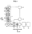
- FIG 1 is a schematic diagram showing one example of a transmission electron microscope equipped with an electron spectrometer being one embodiment according to the present invention.
- the transmission electron microscope equipped with the electron spectrometer of the present embodiment is composed of a transmission electron microscope 1, the electron spectrometer 8, an image display device 14, a central control unit 16, a spectral image distortion correction apparatus 15, and others.
- the transmission electron microscope 1 has an electron source 2 emitting an electron beam 3, condenser lenses 4, an objective lens 6, an imaging lens system 7, a fluorescent screen 9, and so on.
- a sample 5 is disposed between the condenser lenses 4 and the objective lens 6.
- the electron spectrometer 8 has a magnetic sector 10, a drift tube 20, multipole lenses 11, 12, a two-dimensional detector 13, and so on.
- the configuration of the transmission electron microscope 1 and the configuration of the electron spectrometer 8 are not limited to the foregoing.
- the electron spectrometer 8 may be disposed within the transmission electron microscope 1.
- the electron beam 3 emitted by the electrons source 2 passes through the condenser lenses 4 and impinges on the sample 5.
- the electron beam 3 transmitted through the sample 5 passes through the objective lens 6 and through the imaging lens system 7 consisting of plural lenses. Where the fluorescent screen 9 is open, the beam intact passes into the electron spectrometer 8.
- the incident electron beam 3 passes through the multipole lenses 11 and 12 and magnetic sector 10 mounted in the electron spectrometer 8.
- the lenses 11 and 12 are used for focusing, enlargement, demagnification, aberration reduction, and for other purpose of electron energy loss spectra, transmission electron microscope images, and energy-selected images.
- the sector 10 is capable of spectral dispersion according to the amount of energy possessed by the electron beam 3. Then, the beam is acquired as a transmission electron microscope image, two-dimensional elemental distribution image, spectral image, or other image by the two-dimensional detector 13 and then displayed on the image display device 14.
- the magnetic sector 10, multipole lenses 11, 12, and drift tube 20 are controlled by the central control unit 16.
- the central control unit 16 can control switching of the acquisition mode in which a transmission electron microscope image, two-dimensional elemental distribution image, spectral image, or other image is obtained.
- the unit can control change of the focal positions on the x- and y-axes, i.e., switching of the acquisition mode in which the transmission electron microscope image 50 and spectral image 51 as shown in FIG 16 are obtained.
- a field of view limiting slit 17 that is short in the x-axis direction (i.e., the energy dispersion direction) and long in the y-axis direction (i.e., a direction towards a sample measurement position) may be inserted to restrict the location where one wants to obtain the spectral image 51.
- a two-dimensional electron position image formed by the axis of energy loss amount and the axis of positional information is obtained.
- the image is compared with reference electron beam positions by the spectral image distortion correction apparatus 15 and amounts of distortion based on the differences of the electron beam positions are stored.
- the spectral image 51 of the analyzed specimen within the sample 5 is obtained by the two-dimensional detector 13.
- the spectral image 51 of the analyzed specimen is corrected based on the amounts of distortion stored in the spectral image distortion correction apparatus 15 and then stored in a data storage device 18.
- an aperture 19 is inserted into the electron beam path. Also, the electron beam position image is derived while varying the accelerating voltage of the electron beam 3 emitted from the electron source 2 by an accelerating voltage varying device 21.
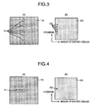
- FIG 3 shows the aperture 19 having plural openings 31 and an electron beam position image 30 obtained by recording the electron beam 3 passed through the openings 31 of the aperture 19 with the two-dimensional detector 13.
- recorded beam positions 32 are recorded in locations close to the left side of the two-dimensional image. No restrictions are imposed on the positions. The positions may be recorded anywhere within the two-dimensional image. Furthermore, no restrictions are placed on the number of the openings 31.
- the electron beam position image 30 is obtained, it is obtained while varying the accelerating voltage by the accelerating voltage varying device 21.
- the electron beam position image 30 may also be obtained while varying the voltage on the drift tube 20 mounted in the electron spectrometer 8.
- the openings 31 in the aperture 19 are arranged in a direction perpendicular to the direction of energy dispersion.
- the shape of each opening 31 is not restricted to circular form.
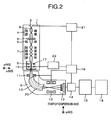
- FIG 2 is an example of transmission electron microscope having an aperture moving device 22.
- the aperture 19 may suffice to have a single opening 31 as shown in FIG 4 , in which case the aperture is movable in a direction perpendicular to the direction of energy dispersion.
- the present aperture moving device 22 may be used as a rotating mechanism for disposing the openings 31 in a direction perpendicular to the direction of energy dispersion.
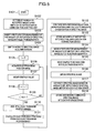
- FIG 5 is a flowchart illustrating a procedure for correcting distortion in a spectral image of a sample to be analyzed after measurement of the amount of the distortion in the spectral image, by the use of the spectral image distortion correction apparatus 15.
- the amount of distortion in the spectral image may be measured using an electron beam transmitted through the measurement position of the spectral image of the sample to be analyzed, in a case where sample damage due to the electron beam is problematic, measurements may also be made using an electron beam transmitted through locations other than the sample to be analyzed.
- the number of accepted electron beam position images 30 and the energy value during the acceptance are set into the central control unit 16.
- the set energy value modifies the accelerating voltage of the electron beam 3 imposed by the accelerating voltage varying device 21, the voltage on the drift tube 20 lying in the electron spectrometer 8, or other value.
- the aperture is inserted into the electron beam path for measurement of the amount of distortion (S101 to S103).
- Electron beam position images 30 are successively derived for each set energy value (S105 to S109).
- each electron beam position 32 is calculated using the aforementioned electron beam position image 30.
- a region close to each electron beam position is specified.
- a maximum value or the position of the center of gravity within the region is taken as an electron beam position (S111). Note that the calculation of the electron beam position is not limited to this method.
- Reference electron beam positions and the electron beam positions found as described just above are compared.
- the amounts of deviation from the reference electron beam positions i.e., the amounts of distortion in the spectral image, are computed and stored in the spectral image distortion correction apparatus 15 (S 112 and S 113).
- the reference line positions are so set that the amounts of energy loss at the positions of the electron beam passed through the openings are identical at each energy value. Furthermore, the reference line positions are so set that the positions of the electron beam passed through the openings are the same Y-position if the energy value is varied.
- a location from which one wants to obtain a spectral image of a sample to be analyzed is moved into the electron beam path, and the desired spectral image 51 is obtained and stored in the spectral image distortion correction apparatus 15. Distortion in the spectral image is corrected based on the amounts of distortion recorded in the spectral image distortion correction apparatus 15. The corrected spectral image is stored in the data storage device 18 (S114 to S118).
- the measurement of the amount of distortion in the present spectral image is preferably carried out immediately prior to acquisition of a spectral image of a desired subject of analysis. Where there is no great variation in the distortion in the spectral image, it is not necessary to obtain a spectral image from each sample whenever a measurement is made.
- the measurement may be carried out only when the instrument is installed and the result may be stored in the spectral image distortion correction apparatus 15.
- FIG 6 shows the electron beam position image 30 displayed on the image display device 14 when the flowchart of FIG 5 is implemented.
- the set energy values are A, B, C, D, and E eV, respectively.
- the number of openings 31 in the aperture 19 is five.
- the set energy value is A eV
- the electron beam position 32 is displayed on the left side of the electron beam position image 30.
- the energy value is changed to B, C, D, and E eV in turn.
- the electron beam position is moved to the right.
- all the electron beam position images 30 are summed up. The resulting image is shown in FIG 7 .
- FIG 8 is an example of display in a case where the electron beam positions 32 are computed from the electron beam position image 30 summed up.
- An electron beam position measurement region 33 for precisely finding the electron beam positions 32 is set near the beam positions 32.
- a maximum value, a value of the center of gravity, or the like within this range is taken as an electron beam position and calculated using the number of pixels of the displayed image.
- FIG 9 is an example of display showing the reference electron beam positions.
- the intersections of reference lines 34 are reference electron beam positions 35. It is possible to instantly judge whether the spectral image is distorted by presenting the present reference lines 34 relative to the sum electron beam position image 30 of all the electron beam position images 30 acquired from the set energy values.
- FIG 10 is an example in which the electron beam position image 30 is shown in a case where there is one opening 31 in the aperture 19. Where there is one opening 31 in the aperture 19, the aperture 19 is moved in the Y-position direction by the aperture moving device 22 for the same energy value as described previously and the electron beam position image 30 is obtained whenever the aperture 19 is moved.
- FIGS. 10(b)-10(f) show electron beam position images 30 when the aperture 19 is moved in the Y-position direction. The electron beam position 32 moves in a corresponding manner to the position of the aperture 19.
- FIG 11 is an example in which the electron beam position image 30 is shown in a case where the energy value is varied under the condition where the aperture 19 has a single opening 31. If the electron beam position image 30 is obtained whenever the energy value is varied from A to E, the electron beam position 32 moves from the left side to the right side. As mentioned previously, even where there is one opening 31 in the aperture 19, it is possible to obtain the electron beam position image 30 for measuring the amount of distortion by changing the energy value while moving the aperture 19 in the Y-position direction by the aperture moving device 22.
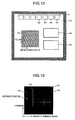
- FIG 12 is a view showing one example of the content of display within the image display device 14.
- a set of select buttons 41 includes a spectral image acceptance starting button 42, a spectral image acceptance ending button 43, a spectral acceptance time change button/spectral image distortion measurement button 44, and a spectral image distortion correction button 45.
- the spectral image acceptance starting button 42 is selected out of the set of select buttons 41, the spectral image 51 is acquired by the two-dimensional detector 13 and displayed within the image display device 14.
- a parameter setting diagram 48 is displayed to set the number of accepted spectra and the energy value for measuring the amount of distortion in each spectral image.
- the electron beam position images 30 are obtained in turn according to the flowchart of FIG 5 .
- the amount of distortion in the spectral image is measured.
- the results of the measurement of the amount of distortion are displayed on a result display diagram 49.
- a spectral image 51 of the sample to be analyzed is acquired.
- the spectral image distortion correction button 45 is selected, the distortion in the spectral image 51 of the sample to be analyzed is corrected and then stored in the data storage device 18.
- the corrected spectral image 51 may be immediately displayed on the image display device 14. If not necessary, the image does not need to be displayed.
- buttons of various functions can be appropriately moved and arranged within the image display device 14.
- the buttons of the functions may be toolbars. Additionally, they may also be arranged at will in the electron beam position image 30, parameter setting diagram 48, or the like displayed within the image display device 14.
- the accelerating voltage of the transmission electron microscope 1 at the time of acquisition of a spectral image was set to 197 kV
- the acceptance angle of the electron beam 3 was set to 4.4 mrad.
- the energy dispersion was set to 0.05 eV/pixel.
- the two-dimensional detector 13 used for the acquisition of the spectral image is a two-dimensional detector of 2048 pixels x 2048 pixels.
- a final magnification on the display of the transmission electron microscope was set to x 10,000.
- the image resolution of the spectral image in the Y-position direction was 0. 2 nm/pixel, the image having been obtained by the two-dimensional detector 13.
- the sample 5 was moved out of the path of the electron beam 3, and the mode was switched to the spectral image mode. Then, adjustments were made such that the multipole lenses 11 and 12 were placed in optimum conditions while referring to the zero loss spectral image displayed on the image display device 14.
- the aperture 19 was inserted into the electron beam path.
- the aperture 19 having five openings in a direction perpendicular to the direction of energy dispersion, i.e., in the Y-position direction, was used.
- the spectral image distortion measurement button 24 was selected, and the number of accepted images and the energy value were set.
- the number of accepted images was set to five, and the widths of the set energy values were set at equal intervals of 80 eV That is, it was determined to acquire electron beam position images at energy values of 0, 40, 80, 120, and 160 eV
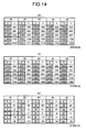
- FIG 13 Shown in FIG 13 is an electron beam position image 30 obtained after summing up all the electron beam position images.
- the reference lines 34 are shown on the electron beam position image 30. It was revealed from the results that the electron beam positions 32 deviated from the reference electron beam positions 35 and that the spectral image was distorted. Therefore, the amount of distortion in the spectral image was measured in detail.
- Electron beam positions at various locations were measured from the electron beam position image 30 obtained in the present specific example, and the results are in FIG 14(a).
- FIG 14(b) shows the reference electron beam positions.
- the amount of distortion was computed from a comparison with the reference electron beam positions.
- Results shown in FIG 14(c) were obtained and stored in the spectral image distortion correction apparatus 15. The present results indicate the amounts of distortion of the reference positions shown in FIG 13 from the electron beam positions.
- the amount of correction can be graphed based on the results of the analysis. For example, the amount of correction can be graphed by plotting energy values on the x-axis, Y-positions on the y-axis, and the amount of correction on the z-axis. Consequently, the amounts of correction at arbitrary energy values and Y-positions can be found.
- FIG 15 A schematic view of the sample used for an analysis is shown in FIG 15 .
- a multilayer film was laminated on a substrate 61 to prepare the sample 5.
- the substrate 61 was silicon.
- the films of the multilayer film 62 on the substrate were silicon oxide (10 nm), silicon nitride (10 nm), and silicon oxide (10 nm) in this order.
- the measured spectral images were close to the absorption edges of the L-shell of silicon.
- the spectral image distortion correction button 45 was selected.
- the distortion in the spectral image was corrected based on the amounts of distortion stored in the spectral image distortion correction apparatus 15.
- a bilinear method was used for the correction of the distortion.
- a correction of the intensity was carried out concomitantly with the distortion correction.
- the present method was used this time.
- the manner in which a distortion is corrected is not restricted to the present technique.
- electron energy loss spectra at various locations corresponding to transmission electron microscope images were obtained all accurately.
- spectral images were obtained after adjusting the multipole lenses 11 and 12 in the electron spectrometer to optimum conditions. Even where no adjustment is made, a similar correction to distortion in spectral images can be made.
- the multipole lenses 11 and 12 in the electron spectrometer may be readjusted based on the amounts of distortion. Then, a desired spectral image may be obtained.
- one spectral image was acquired in an acceptance time of 20 seconds.
- S/N signal-to-noise ratio
- plural spectral images may be obtained and then corrections may be made for drift (movement) in the direction of energy of the spectral image and for drift (movement) in the positional direction.
- the spectral images may be summed up.
- the acceptance time and the number of accepted images can be set at will in the central control unit 16. Distortion correction of spectral image by the spectral image distortion correction apparatus 15 is carried out for each obtained spectral image. Then, drift between the distortion-corrected spectral images may be corrected and then the images may be summed up.
- all the spectral images may be corrected for drift and summed up and then a distortion correction may be carried out.
- the acquisition time in which a single spectral image is obtained is preferably set to such a time that the effects of energy drift and sample drift are small.
Landscapes
- Chemical & Material Sciences (AREA)
- Analytical Chemistry (AREA)
- Analysing Materials By The Use Of Radiation (AREA)
Applications Claiming Priority (2)
| Application Number | Priority Date | Filing Date | Title |
|---|---|---|---|
| JP2008312809A JP5315033B2 (ja) | 2008-12-09 | 2008-12-09 | 電子分光器を備えた透過型電子顕微鏡 |
| PCT/JP2009/005999 WO2010067512A1 (fr) | 2008-12-09 | 2009-11-11 | Microscope électronique à transmission avec spectromètre électronique |
Publications (2)
| Publication Number | Publication Date |
|---|---|
| EP2375436A1 true EP2375436A1 (fr) | 2011-10-12 |
| EP2375436A4 EP2375436A4 (fr) | 2012-07-04 |
Family
ID=42242510
Family Applications (1)
| Application Number | Title | Priority Date | Filing Date |
|---|---|---|---|
| EP09831620A Withdrawn EP2375436A4 (fr) | 2008-12-09 | 2009-11-11 | Microscope électronique à transmission avec spectromètre électronique |
Country Status (4)
| Country | Link |
|---|---|
| US (1) | US8436301B2 (fr) |
| EP (1) | EP2375436A4 (fr) |
| JP (1) | JP5315033B2 (fr) |
| WO (1) | WO2010067512A1 (fr) |
Cited By (1)
| Publication number | Priority date | Publication date | Assignee | Title |
|---|---|---|---|---|
| EP3196920A1 (fr) * | 2016-01-20 | 2017-07-26 | Gatan, Inc. | Spectromètre de perte d'énergie d'électrons utilisant un capteur de détection directe |
Families Citing this family (10)
| Publication number | Priority date | Publication date | Assignee | Title |
|---|---|---|---|---|
| JP5315033B2 (ja) * | 2008-12-09 | 2013-10-16 | 株式会社日立ハイテクノロジーズ | 電子分光器を備えた透過型電子顕微鏡 |
| EP2461348A1 (fr) * | 2010-12-06 | 2012-06-06 | FEI Company | Système de détecteur à utiliser avec une spectroscopie de microscope électronique à transmission |
| US9831061B2 (en) | 2013-12-09 | 2017-11-28 | North Carolina State University | Methods, systems, and computer readable media for measuring and correcting drift distortion in images obtained using a scanning microscope |
| JP6429677B2 (ja) * | 2015-02-27 | 2018-11-28 | 日本電子株式会社 | 測定方法および電子顕微鏡 |
| CN107796837B (zh) * | 2017-10-09 | 2019-10-29 | 南京大学 | 一种成像装置、成像方法及成像系统 |
| US11698336B2 (en) * | 2019-09-30 | 2023-07-11 | Jeol Ltd. | Analysis method and analysis apparatus |
| CN115398592A (zh) * | 2020-04-03 | 2022-11-25 | Asml荷兰有限公司 | 基于带电粒子束检查中的电荷累积减少的图像增强 |
| EP4002420A1 (fr) * | 2020-11-12 | 2022-05-25 | FEI Company | Procédé de détermination d'une largeur d'énergie d'un faisceau de particules chargées |
| JP7673010B2 (ja) * | 2022-03-22 | 2025-05-08 | 株式会社日立ハイテク | 光電子顕微鏡 |
| US20240201112A1 (en) * | 2022-12-14 | 2024-06-20 | Gatan, Inc. | System and method of operating an electron energy loss spectrometer |
Family Cites Families (19)
| Publication number | Priority date | Publication date | Assignee | Title |
|---|---|---|---|---|
| US5414261A (en) * | 1993-07-01 | 1995-05-09 | The Regents Of The University Of California | Enhanced imaging mode for transmission electron microscopy |
| US6184524B1 (en) * | 1996-08-07 | 2001-02-06 | Gatan, Inc. | Automated set up of an energy filtering transmission electron microscope |
| US5798524A (en) * | 1996-08-07 | 1998-08-25 | Gatan, Inc. | Automated adjustment of an energy filtering transmission electron microscope |
| WO1998038669A1 (fr) * | 1997-02-28 | 1998-09-03 | Arizona Board Of Regents | Dispositifs atomiques de focalisation en microscopie electronique |
| JP3780620B2 (ja) * | 1997-04-25 | 2006-05-31 | 株式会社日立製作所 | 電子分光器及びそれを備えた透過型電子顕微鏡 |
| JP3518271B2 (ja) * | 1997-08-28 | 2004-04-12 | 株式会社日立製作所 | エネルギーフィルタおよびこれを備えた電子顕微鏡 |
| EP1209720A3 (fr) | 2000-11-21 | 2006-11-15 | Hitachi High-Technologies Corporation | Mesure de spectre en énergie |
| JP3726673B2 (ja) * | 2000-11-21 | 2005-12-14 | 株式会社日立製作所 | エネルギースペクトル測定装置,電子エネルギー損失分光装置、及びそれを備えた電子顕微鏡、及び電子エネルギー損失スペクトル測定方法 |
| JP2003022774A (ja) * | 2001-07-06 | 2003-01-24 | Hitachi Ltd | 透過型電子顕微鏡 |
| JP3979945B2 (ja) * | 2003-01-23 | 2007-09-19 | 日本電子株式会社 | 電子分光系を有した電子線装置 |
| JP2006196236A (ja) * | 2005-01-12 | 2006-07-27 | Hitachi High-Technologies Corp | 電子顕微鏡及び観察方法 |
| JP4399471B2 (ja) * | 2007-02-28 | 2010-01-13 | 株式会社日立ハイテクノロジーズ | 電子分光器を備えた透過型電子顕微鏡 |
| JP4997013B2 (ja) * | 2007-07-31 | 2012-08-08 | 株式会社日立ハイテクノロジーズ | 電子分光器を備えた電子顕微鏡 |
| US7777185B2 (en) * | 2007-09-25 | 2010-08-17 | Ut-Battelle, Llc | Method and apparatus for a high-resolution three dimensional confocal scanning transmission electron microscope |
| JP5449679B2 (ja) * | 2008-02-15 | 2014-03-19 | 株式会社日立製作所 | 電子線観察装置および試料観察方法 |
| JP4474473B2 (ja) * | 2008-03-31 | 2010-06-02 | 株式会社日立ハイテクノロジーズ | 電子分光器を備えた透過型電子顕微鏡 |
| US8203120B2 (en) * | 2008-10-09 | 2012-06-19 | California Institute Of Technology | 4D imaging in an ultrafast electron microscope |
| JP5315033B2 (ja) * | 2008-12-09 | 2013-10-16 | 株式会社日立ハイテクノロジーズ | 電子分光器を備えた透過型電子顕微鏡 |
| JP5462875B2 (ja) * | 2009-07-16 | 2014-04-02 | 株式会社日立ハイテクノロジーズ | 荷電粒子線顕微鏡及びそれを用いた測定方法 |
-
2008
- 2008-12-09 JP JP2008312809A patent/JP5315033B2/ja not_active Expired - Fee Related
-
2009
- 2009-11-11 EP EP09831620A patent/EP2375436A4/fr not_active Withdrawn
- 2009-11-11 US US13/133,653 patent/US8436301B2/en not_active Expired - Fee Related
- 2009-11-11 WO PCT/JP2009/005999 patent/WO2010067512A1/fr not_active Ceased
Cited By (2)
| Publication number | Priority date | Publication date | Assignee | Title |
|---|---|---|---|---|
| EP3196920A1 (fr) * | 2016-01-20 | 2017-07-26 | Gatan, Inc. | Spectromètre de perte d'énergie d'électrons utilisant un capteur de détection directe |
| US9966220B2 (en) | 2016-01-20 | 2018-05-08 | Gatan, Inc. | Electron energy loss spectrometer using direct detection sensor |
Also Published As
| Publication number | Publication date |
|---|---|
| WO2010067512A1 (fr) | 2010-06-17 |
| JP5315033B2 (ja) | 2013-10-16 |
| US20110240854A1 (en) | 2011-10-06 |
| JP2010140640A (ja) | 2010-06-24 |
| US8436301B2 (en) | 2013-05-07 |
| EP2375436A4 (fr) | 2012-07-04 |
Similar Documents
| Publication | Publication Date | Title |
|---|---|---|
| US8436301B2 (en) | Transmission electron microscope having electron spectrometer | |
| EP1965407B1 (fr) | Microscope à électrons de transmission fourni avec un spectroscope électronique | |
| US9558910B2 (en) | Sample holder for electron microscope | |
| US8263936B2 (en) | Transmission electron microscope having electron spectroscope | |
| US10134558B2 (en) | Scanning electron microscope | |
| JPWO2000041206A1 (ja) | 元素マッピング装置、走査透過型電子顕微鏡および元素マッピング方法 | |
| JP3979945B2 (ja) | 電子分光系を有した電子線装置 | |
| WO2003038418A1 (fr) | Dispositif d'analyses d'elements, microscope electronique a emission par balayage et procede d'analyses d'elements | |
| EP3203493A1 (fr) | Microscope à particules chargées avec compensation d'astigmatisme et sélection d'energie | |
| US9589761B2 (en) | Electron microscope and method of adjusting same | |
| US6930306B2 (en) | Electron microscope | |
| JP6266467B2 (ja) | 電子顕微鏡、およびモノクロメーターの調整方法 | |
| EP2293319B1 (fr) | Appareil de microscope électronique à transmission comprenant un spectroscope électronique, un support d'échantillon, un étage d'échantillon, et procédé d'acquisition d'une image spectrale | |
| JP2001307672A (ja) | 元素分析装置及び走査透過型電子顕微鏡並びに元素分析方法 | |
| US20030085350A1 (en) | Ultimate analyzer, scanning transmission electron microscope and ultimate analysis method | |
| JP4449573B2 (ja) | 元素マッピング装置,走査透過型電子顕微鏡および元素マッピング方法 | |
| JP5470408B2 (ja) | 電子分光器を有する透過型電子顕微鏡装置,試料ホルダ,試料台及びスペクトル像の取得方法 | |
| JP2005302335A (ja) | 電子線エネルギー分光装置及びそれを備えた電子顕微鏡 | |
| JP4512514B2 (ja) | 電子線分光器を備えた透過型電子顕微鏡 |
Legal Events
| Date | Code | Title | Description |
|---|---|---|---|
| PUAI | Public reference made under article 153(3) epc to a published international application that has entered the european phase |
Free format text: ORIGINAL CODE: 0009012 |
|
| 17P | Request for examination filed |
Effective date: 20110708 |
|
| AK | Designated contracting states |
Kind code of ref document: A1 Designated state(s): AT BE BG CH CY CZ DE DK EE ES FI FR GB GR HR HU IE IS IT LI LT LU LV MC MK MT NL NO PL PT RO SE SI SK SM TR |
|
| DAX | Request for extension of the european patent (deleted) | ||
| A4 | Supplementary search report drawn up and despatched |
Effective date: 20120601 |
|
| RIC1 | Information provided on ipc code assigned before grant |
Ipc: H01J 37/05 20060101AFI20120525BHEP Ipc: H01J 37/153 20060101ALI20120525BHEP Ipc: H01J 37/26 20060101ALI20120525BHEP |
|
| STAA | Information on the status of an ep patent application or granted ep patent |
Free format text: STATUS: THE APPLICATION HAS BEEN WITHDRAWN |
|
| 18W | Application withdrawn |
Effective date: 20151102 |