EP2375451A2 - Seitengraben-Feldeffektortransistoren in Halbleitermaterialien mit weitem Bandabstand, Herstellungsverfahren dafür und integrierte Schaltungen mit den Transistoren - Google Patents
Seitengraben-Feldeffektortransistoren in Halbleitermaterialien mit weitem Bandabstand, Herstellungsverfahren dafür und integrierte Schaltungen mit den Transistoren Download PDFInfo
- Publication number
- EP2375451A2 EP2375451A2 EP11173329A EP11173329A EP2375451A2 EP 2375451 A2 EP2375451 A2 EP 2375451A2 EP 11173329 A EP11173329 A EP 11173329A EP 11173329 A EP11173329 A EP 11173329A EP 2375451 A2 EP2375451 A2 EP 2375451A2
- Authority
- EP
- European Patent Office
- Prior art keywords
- layer
- semiconductor material
- drain
- source
- substrate
- Prior art date
- Legal status (The legal status is an assumption and is not a legal conclusion. Google has not performed a legal analysis and makes no representation as to the accuracy of the status listed.)
- Withdrawn
Links
Images


Classifications
-
- H—ELECTRICITY
- H10—SEMICONDUCTOR DEVICES; ELECTRIC SOLID-STATE DEVICES NOT OTHERWISE PROVIDED FOR
- H10D—INORGANIC ELECTRIC SEMICONDUCTOR DEVICES
- H10D30/00—Field-effect transistors [FET]
- H10D30/80—FETs having rectifying junction gate electrodes
-
- H—ELECTRICITY
- H10—SEMICONDUCTOR DEVICES; ELECTRIC SOLID-STATE DEVICES NOT OTHERWISE PROVIDED FOR
- H10D—INORGANIC ELECTRIC SEMICONDUCTOR DEVICES
- H10D30/00—Field-effect transistors [FET]
- H10D30/80—FETs having rectifying junction gate electrodes
- H10D30/83—FETs having PN junction gate electrodes
-
- H—ELECTRICITY
- H10—SEMICONDUCTOR DEVICES; ELECTRIC SOLID-STATE DEVICES NOT OTHERWISE PROVIDED FOR
- H10D—INORGANIC ELECTRIC SEMICONDUCTOR DEVICES
- H10D30/00—Field-effect transistors [FET]
- H10D30/80—FETs having rectifying junction gate electrodes
- H10D30/87—FETs having Schottky gate electrodes, e.g. metal-semiconductor FETs [MESFET]
- H10D30/871—Vertical FETs having Schottky gate electrodes
-
- H—ELECTRICITY
- H10—SEMICONDUCTOR DEVICES; ELECTRIC SOLID-STATE DEVICES NOT OTHERWISE PROVIDED FOR
- H10D—INORGANIC ELECTRIC SEMICONDUCTOR DEVICES
- H10D62/00—Semiconductor bodies, or regions thereof, of devices having potential barriers
- H10D62/80—Semiconductor bodies, or regions thereof, of devices having potential barriers characterised by the materials
- H10D62/83—Semiconductor bodies, or regions thereof, of devices having potential barriers characterised by the materials being Group IV materials, e.g. B-doped Si or undoped Ge
- H10D62/832—Semiconductor bodies, or regions thereof, of devices having potential barriers characterised by the materials being Group IV materials, e.g. B-doped Si or undoped Ge being Group IV materials comprising two or more elements, e.g. SiGe
- H10D62/8325—Silicon carbide
-
- H—ELECTRICITY
- H10—SEMICONDUCTOR DEVICES; ELECTRIC SOLID-STATE DEVICES NOT OTHERWISE PROVIDED FOR
- H10D—INORGANIC ELECTRIC SEMICONDUCTOR DEVICES
- H10D62/00—Semiconductor bodies, or regions thereof, of devices having potential barriers
- H10D62/80—Semiconductor bodies, or regions thereof, of devices having potential barriers characterised by the materials
- H10D62/85—Semiconductor bodies, or regions thereof, of devices having potential barriers characterised by the materials being Group III-V materials, e.g. GaAs
- H10D62/8503—Nitride Group III-V materials, e.g. AlN or GaN
-
- H—ELECTRICITY
- H10—SEMICONDUCTOR DEVICES; ELECTRIC SOLID-STATE DEVICES NOT OTHERWISE PROVIDED FOR
- H10D—INORGANIC ELECTRIC SEMICONDUCTOR DEVICES
- H10D64/00—Electrodes of devices having potential barriers
- H10D64/60—Electrodes characterised by their materials
- H10D64/64—Electrodes comprising a Schottky barrier to a semiconductor
-
- H—ELECTRICITY
- H10—SEMICONDUCTOR DEVICES; ELECTRIC SOLID-STATE DEVICES NOT OTHERWISE PROVIDED FOR
- H10D—INORGANIC ELECTRIC SEMICONDUCTOR DEVICES
- H10D84/00—Integrated devices formed in or on semiconductor substrates that comprise only semiconducting layers, e.g. on Si wafers or on GaAs-on-Si wafers
- H10D84/80—Integrated devices formed in or on semiconductor substrates that comprise only semiconducting layers, e.g. on Si wafers or on GaAs-on-Si wafers characterised by the integration of at least one component covered by groups H10D12/00 or H10D30/00, e.g. integration of IGFETs
- H10D84/87—Integrated devices formed in or on semiconductor substrates that comprise only semiconducting layers, e.g. on Si wafers or on GaAs-on-Si wafers characterised by the integration of at least one component covered by groups H10D12/00 or H10D30/00, e.g. integration of IGFETs of PN-junction gate FETs
Definitions
- the present invention relates generally to lateral field effect transistors (FETS) with vertical channels, and in particular, to such transistors formed in wide bandgap semiconductor materials. This invention also relates to monolithic integrated circuits comprising these transistors.
- FETS lateral field effect transistors
- Wide bandgap semiconductor materials such as silicon carbide (SiC) or Group III nitride compound semiconductors (e.g ., gallium nitride GaN) are very attractive for use in high-power, high-temperature, and/or radiation resistant electronics.
- SiC power rectifiers and RF transistors are now commercially available, and SiC power switches as well as GaN microwave transistors are expected to appear in the commercial market in the near future,
- CMOS Complementary Metal-Oxide-Semiconductor
- DCFL Direct Coupled FET Logic
- MOSFETs SiC Lateral DMOS Field-Effect Transistors
- LDMOSFETs SiC Lateral DMOS Field-Effect Transistors
- certain issues limit the use of MOSFET-based SiC integrated circuits in the applications where high temperature and/or radiation tolerance is required.
- the first such issue is on-state insulator reliability due to much smaller conduction band offset of SiC to SiO 2 as compared to that of silicon [6], [7]. This issue becomes even more significant at high temperature and extreme radiation environment.
- Other issues include: low inversion channel mobility due to high interface state density at the SiC/SiO 2 interface and high fixed charge density in the insulator; and significant threshold voltage shift with temperature due to ionization of interface states.
- SiC MESFET Metal Semiconductor Field-Effect Transistor
- JFET-based ICs An alternative to the MOSFET and MESFET approaches is the use of lateral JFET-based ICs.
- An example of a vertical channel JFET employing a recessed gate structure can be found in U.S. Patent No. 4,587,712 [10].
- An example of a lateral JFET formed in SiC can be found in U. S. Patent No. 5,264,713 [11].
- Enhanced-mode JFET digital IGs with resistive load have also been reported [12].
- JFET based ICs can also be implemented in either complementary (n-type and p-type channels as disclosed in U.S. Patent No. 6,503,782 [13] or enhanced-depletion (n-type channels) forms.
- SiC JFETs have proven to be radiation tolerant while demonstrating very insignificant threshold voltage shift with temperature [14]. A major deficiency of this approach has been difficulties achieving monolithic integration of low voltage control circuitry with power switches for Smart Power electronics.
- a junction field-effect transistor which comprises:
- the source region can be coextensive with the channel region.
- a semiconductor device which comprises:
- the first junction field-effect transistor can have a first threshold voltage and the second junction field-effect transistor can have a second threshold voltage different than the first threshold voltage
- a field-effect transistor which comprises:
- the field-effect transistor according to any of the aforementioned embodiments can comprise a plurality of raised regions.
- the raised regions can be elongate, having a major and a minor dimension.
- the raised regions can be oriented such that the major dimensions of the raised regions are parallel to one another.
- the plurality of raised source regions can also be spaced apart from one another at regular intervals in the direction of the minor dimension.
- the gate region can comprise a plurality of fingers extending between adjacent raised regions.
- a field-effect transistor which comprises:
- the semiconductor material of the drain layer, drift layer, gate region, channel region and source region can have an E G of at least 2 eV (e.g ., SiC or a Group III nitride compound semiconductor material such as GaN).
- the substrate can be selected from the group consisting of: semi-insulating; p-type; or n-type with a p-type buffer layer thereon wherein the p-type buffer layer forms the first surface of the substrate.
- an integrated circuit which comprises a plurality of field-effect transistors as set forth in any of the aforementioned embodiments disposed on a common substrate.
- the integrated circuit can comprise a first field-effect transistor having a first threshold voltage and a second field-effect transistor having a second threshold voltage different than the first threshold voltage.
- a method of making a field-effect transistor comprises selectively etching a multi-layered structure.
- the multi-layered structure comprises: a substrate having opposed first and second surfaces; a drain layer of an n-type semiconductor material on the first surface of the substrate; a drift layer of an n-type semiconductor material non the drain layer, the drift layer having a lower conductivity than the drain layer; a channel layer of an n-type semiconductor material on the drift layer between and in contact with adjacent gate regions; and a source layer of an n-type semiconductor material on the channel region, the source layer having a higher conductivity than the channel layer.
- the method according to this embodiment comprises selectively etching through the source layer and partially through the channel layer to form at least one raised region; selectively implanting ions of a p-type dopant in exposed portions of the channel layer adjacent the at least one raised region; selectively etching through exposed portions of the implanted channel layer and underlying drift layer to expose underlying drain layer; and selectively etching through exposed portions of the drain layer to expose underlying substrate thereby forming an etched structure.
- a method of making a field-effect transistor comprises selectively implanting a p-type dopant on a multi-layered structure.
- the multi-layered structure comprises: a substrate having opposed first and second major surfaces; a drain layer of an n-type semiconductor material on the first major surface of the substrate; a drift layer of an n-type semiconductor material on the drain layer, the drift layer having a lower conductivity than the drain layer.
- the method according to this embodiment comprises selectively implanting the p-type dopant in the drift layer to form a gate region; depositing or growing a channel layer of an n-type semiconductor material on the implanted surface of the drift layer; depositing or growing a source layer of an n-type semiconductor material on the channel layer, the source layer having a higher conductivity than the channel layer; selectively etching through the source layer, the channel layer and the implanted drift layer to expose underlying drain layer thereby forming raised regions; and selectively etching through portions of the exposed drain layer to expose underlying substrate thereby forming an etched structure.
- a method of making a field-effect transistor comprises selectively etching a multi-layered structure.
- the multi-layered structure comprises: a substrate having opposed first and second major surfaces; a drain layer of an n-type semiconductor material on the first major surface of the substrate; a drift layer of an n-type semiconductor material on the drain layer, the drift layer having a lower conductivity than the drain layer; a channel layer of an n-type semiconductor material on the drift layer; and a source layer of an n-type semiconductor material on the channel region, the source layer having a higher conductivity than the channel layer.
- the method according to this embodiment comprises selectively etching through the source and channel layers to expose underlying drift layer thereby forming at least one raised region; selectively etching through exposed portions of the drift layer to expose underlying drain layer; selectively etching through exposed portions of the drain layer to expose underlying substrate, thereby forming an etched structure; and depositing a Schottky metal in contact with exposed portions of the drift layer.
- a method according to any of the aforementioned embodiments may further comprise an annealing treatment after the implantation of the p-type dopant in order to activate the dopant.
- a method according to any of the aforementioned embodiments may further comprise growing or depositing a layer of dielectric material on exposed surfaces of the etched structure; anisotropically etching the dielectric material to expose underlying portions of drain, gate and/or source regions parallel to the first surface of the substrate; and depositing metal on exposed portions of drain, gate and source regions.
- the semiconductor material can be SiC.
- the method can further comprise annealing after depositing metal on exposed portions of drain, gate and/or source regions such that metal at the metal/semiconductor material interface reacts to form metal silicide; and removing unreacted metal.
- the unreacted metal can be removed using an acid etch.
- a plurality of raised regions can be formed.
- the plurality of raised regions can be elongate and can have a major and a minor dimension.
- the raised regions can be oriented such that the major dimensions of the raised source regions are parallel to one another.
- the plurality of raised source regions can be spaced apart from one another at regular intervals in the direction of the minor dimension.
- multiple etched structures can be formed on a single substrate wherein etching through the drain layer isolates each etched structure.
- JFET vertical channel Junction Field-Effect Transistor
- the present invention relates generally to Junction Field-Effect Transistors (JFETs) with vertical channel and monolithic integrated circuits fabricated using such devices.
- JFETs Junction Field-Effect Transistors
- the present invention relates to such transistors and circuits formed in wide bandgap semiconductor materials.
- the present device can be built on a wide bandgap (i.e ., E G >2 eV) semiconductor substrate, which can be either semi-insulating, p-type, or n-type with a p-type buffer layer.
- the device can comprise source, channel, drift and drain epitaxially grown n-type layers, as well as p-type implanted gate regions.
- the device structure can be defined using plasma etch and ion implantation, and the ohmic contacts to the source, gate, and drain regions can be formed on the same side of the wafer.
- the JFET may have different threshold voltages, and can be implemented for both depletion and enhanced modes of operation for the same channel doping.
- the devices with different threshold voltages can be used for both digital and analog integrated circuits.
- the devices described above can be used in monolithic microwave integrated circuits (MMICs).
- Silicon carbide crystallizes in numerous (i.e ., more than 200) different modifications (polytypes).
- the most important polytypes are: 3C-SiC (cubic unit cell, zincblende); 2H-SiC; 4H-SiC; 6H-SiC (hexagonal unit cell, wurtzile); 15R-SiC (rhombohedral unit cell).
- the 4H polytype is more attractive for power devices, however, because of its higher electron mobility.
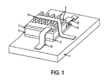
- FIG. 1 an example schematic 3-dimensional view is shown of semiconductor device referred to as Lateral Trench Junction Field-Effect Transistor (LTJFET).
- the described device is built on the wide bandgap semiconductor substrate (1), which can be either semi-insulating, p-type, or n-type with p-type buffer layer.
- the device comprises source, channel, drift (3) and drain (2) epitaxially grown n-type layers, as well as p-type implanted gate regions (7).
- the device structure shown in Figure 1 is defined using plasma etch and ion implantation, and the ohmic contacts (9) to the source, gate, and drain regions are formed on the same side of the wafer.
- Source (11), drain (12) and gate (13) interconnects are also shown in Figure 1 .
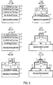
- FIG. 2 is a schematic representing an exemplary fabrication method for a single-finger LTJFET built on a semi-insulating substrate.
- an epitaxial stack is grown on a semi-insulating substrate in fabrication step A.
- an etch/implantation mask (6) is formed on the surface of the top epitaxial layer.
- the source and the channel regions are defined by sequential plasma etch steps through layer (5) and partially through layer (4), followed by implantation of Al + or B + ions to form p-type gate regions (7).
- step D sequential plasma etch steps are used to expose heavily doped drain layer (2) by etching through the gate region (7) and drift layer (3), and to form mesa isolation by etching through layer (2) into semi-insulating substrate (1).
- step E a thin layer of dielectric (8) is either grown or deposited on the surface that has resulted from the previous fabrication steps.
- An anisotropic plasma etch is then performed in fabrication step F to expose semiconductor material on the horizontal areas of the device by etching through the thin dielectric layer.
- This etch step can be followed by metal deposition and high temperature ohmic contact anneal to form metal silicide in the areas where metal touches semiconductor material. After the silicide formation, the unreacted metal can removed ( e.g ., using acid etch).
- Figures 3A and 3B are schematic cross-sectional representations of LTJFETs fabricated on conducting substrates and isolated from the other devices fabricated on the same die by a p-n junction.
- Figure 3A shows a schematic cross-section of a single-finger LTJFET fabricated on p-type substrate using the fabrication process presented in Figure 2 .
- the LTJFET can also be fabricated on an n-type substrate.
- this device comprises an additional p-type epitaxially grown layer to provide p-n junction isolation.
- GaN n-type epitaxial layers can be grown on silicon carbide, sapphire, or silicon substrates to form a starting material stack for the fabrication of the device structure.
- a substrate material comprising a conducting SiC substrate with semi-insulating epitaxially grown buffer layer can be used.
- Such a device is described in U.S. Patent Application No. 10/033,785, filed January 3, 2002 , published as U.S. Patent Publication No. 2002-0149021 [15], which application is incorporated by reference herein in its entirety.
- a substrate material e.g ., AIN, Al 2 O 3 , BeO, etc.
- AIN Al 2 O 3 , BeO, etc.
- FIGS. 4A and 4B are schematic cross-sections of FETs fabricated on semi-insulating substrates with alternative structures for the vertical channel.
- Figure 4A shows a schematic cross-section of a single-channel JFET, where the channel region is defined by p-type implantation followed by epitaxial growth of n-type layers. Examples of how to form an overgrown source region in a vertical JFET structure can be found in U.S. Patent No. 5,610,085 [16].
- a lateral trench FET can also be fabricated implementing a Schottky gate instead of an ion-implanted p-type gate. Examples of how to form a Schottky gate in a trench structure can be found in U.S. Patent Nos. 6,156,611 and 5,945,701 [17], [18].
- Figures 5A and 5B are schematic cross-sectional representations of single-finger and multi-finger Lateral Trench JFETs fabricated on a semi-insulating substrate including schematic depictions of electrical connections to the source, drain, and gate terminals.
- LTJFETs fabricated on the same die may have vertical channels of different widths (i.e ., widths of source fingers) that would result in different threshold voltages.
- the possibility to define device threshold voltage by layout design provides an additional flexibility for the design of monolithic integrated circuits. For example, having multiple threshold voltages on the same chip enables more flexibility and higher integrity for RF designs. Such flexibility can be very difficult to achieve, for example, in the case of devices with lateral channels such as MOSFETs or lateral JFETs.
- Figure 6A provides a schematic cross-section of two single-finger Lateral Trench JFETs fabricated on the same die with different vertical channel widths.
- Figure 6B is a schematic showing a monolithic inverter circuit using the devices depicted in Figure 6A .
- the SiC layers can be formed by doping the layers with donor or acceptor materials using known techniques.
- exemplary donor materials include nitrogen and phosphorus. Nitrogen is a preferred donor material.
- exemplary acceptor materials for doping SiC include boron and aluminum. Aluminum is a preferred acceptor material.
- the above materials are merely exemplary, however, and any acceptor and donor materials which can be doped into silicon carbide can be used.
- the dop bing levels and thicknesses of the various layers of the Lateral Trench JFET described herein can be varied to produce a device having desired characteristics for a particular application. Similarly, the dimensions of the various features of the device can also be varied to produce a device having desired characteristics for a particular application.
- the SiC layers can be formed by epitaxial growth on a suitable substrate.
- the layers can be doped during epitaxial growth.
- heavily doped (++) in the context of the invention corresponds to dopant concentrations of 10 18 atoms•cm -3 or greater
- lightly doped (-) corresponds to dopant concentrations of 5x10 16 atoms•cm -3 or less
- moderately doped (+) corresponds to dopant concentrations of between 5x10 16 atoms•cm -3 and 10 18 atoms•cm -3 .
Landscapes
- Junction Field-Effect Transistors (AREA)
- Insulated Gate Type Field-Effect Transistor (AREA)
- Metal-Oxide And Bipolar Metal-Oxide Semiconductor Integrated Circuits (AREA)
- Electrodes Of Semiconductors (AREA)
Applications Claiming Priority (2)
| Application Number | Priority Date | Filing Date | Title |
|---|---|---|---|
| US10/999,954 US7119380B2 (en) | 2004-12-01 | 2004-12-01 | Lateral trench field-effect transistors in wide bandgap semiconductor materials, methods of making, and integrated circuits incorporating the transistors |
| EP05852246A EP1825522A4 (de) | 2004-12-01 | 2005-11-30 | Seitengraben-feldeffekttransistoren in hableitermaterialien mit weitem bandabstand, herstellungsverfahren dafür und integrierte schaltungen mit den transistoren |
Related Parent Applications (1)
| Application Number | Title | Priority Date | Filing Date |
|---|---|---|---|
| EP05852246.7 Division | 2005-11-30 |
Publications (2)
| Publication Number | Publication Date |
|---|---|
| EP2375451A2 true EP2375451A2 (de) | 2011-10-12 |
| EP2375451A3 EP2375451A3 (de) | 2012-04-18 |
Family
ID=36565582
Family Applications (2)
| Application Number | Title | Priority Date | Filing Date |
|---|---|---|---|
| EP11173329A Withdrawn EP2375451A3 (de) | 2004-12-01 | 2005-11-30 | Seitengraben-Feldeffektortransistoren in Halbleitermaterialien mit weitem Bandabstand, Herstellungsverfahren dafür und integrierte Schaltungen mit den Transistoren |
| EP05852246A Withdrawn EP1825522A4 (de) | 2004-12-01 | 2005-11-30 | Seitengraben-feldeffekttransistoren in hableitermaterialien mit weitem bandabstand, herstellungsverfahren dafür und integrierte schaltungen mit den transistoren |
Family Applications After (1)
| Application Number | Title | Priority Date | Filing Date |
|---|---|---|---|
| EP05852246A Withdrawn EP1825522A4 (de) | 2004-12-01 | 2005-11-30 | Seitengraben-feldeffekttransistoren in hableitermaterialien mit weitem bandabstand, herstellungsverfahren dafür und integrierte schaltungen mit den transistoren |
Country Status (9)
| Country | Link |
|---|---|
| US (2) | US7119380B2 (de) |
| EP (2) | EP2375451A3 (de) |
| JP (1) | JP5417585B2 (de) |
| KR (1) | KR101224810B1 (de) |
| CN (1) | CN101317271B (de) |
| AU (1) | AU2005312118B2 (de) |
| CA (1) | CA2589028A1 (de) |
| NZ (1) | NZ555625A (de) |
| WO (1) | WO2006060302A2 (de) |
Families Citing this family (34)
| Publication number | Priority date | Publication date | Assignee | Title |
|---|---|---|---|---|
| US7642566B2 (en) * | 2006-06-12 | 2010-01-05 | Dsm Solutions, Inc. | Scalable process and structure of JFET for small and decreasing line widths |
| US8193612B2 (en) * | 2004-02-12 | 2012-06-05 | International Rectifier Corporation | Complimentary nitride transistors vertical and common drain |
| US7820511B2 (en) * | 2004-07-08 | 2010-10-26 | Semisouth Laboratories, Inc. | Normally-off integrated JFET power switches in wide bandgap semiconductors and methods of making |
| US20070029573A1 (en) * | 2005-08-08 | 2007-02-08 | Lin Cheng | Vertical-channel junction field-effect transistors having buried gates and methods of making |
| US7745851B2 (en) * | 2006-04-13 | 2010-06-29 | Cree, Inc. | Polytype hetero-interface high electron mobility device and method of making |
| US7274083B1 (en) * | 2006-05-02 | 2007-09-25 | Semisouth Laboratories, Inc. | Semiconductor device with surge current protection and method of making the same |
| US8269262B2 (en) * | 2006-05-02 | 2012-09-18 | Ss Sc Ip Llc | Vertical junction field effect transistor with mesa termination and method of making the same |
| US8421119B2 (en) * | 2006-09-13 | 2013-04-16 | Rohm Co., Ltd. | GaN related compound semiconductor element and process for producing the same and device having the same |
| JP2008118082A (ja) * | 2006-10-11 | 2008-05-22 | New Japan Radio Co Ltd | 窒化物半導体装置及びその製造方法 |
| US7501670B2 (en) | 2007-03-20 | 2009-03-10 | Velox Semiconductor Corporation | Cascode circuit employing a depletion-mode, GaN-based FET |
| US7688117B1 (en) | 2008-04-21 | 2010-03-30 | The United States Of America As Represented By The Administrator Of National Aeronautics And Space Administration | N channel JFET based digital logic gate structure |
| NZ597036A (en) * | 2009-06-19 | 2014-01-31 | Power Integrations Inc | Methods of making vertical junction field effect transistors and bipolar junction transistors without ion implantation and devices made therewith |
| CN102054699B (zh) * | 2009-11-05 | 2012-07-25 | 中芯国际集成电路制造(上海)有限公司 | 改善半导体器件结深特性的方法 |
| JP2011119512A (ja) * | 2009-12-04 | 2011-06-16 | Denso Corp | 半導体装置およびその製造方法 |
| US8236640B2 (en) * | 2009-12-18 | 2012-08-07 | Intel Corporation | Method of fabricating a semiconductor device having gate finger elements extended over a plurality of isolation regions formed in the source and drain regions |
| JP4985757B2 (ja) * | 2009-12-25 | 2012-07-25 | 株式会社デンソー | 炭化珪素半導体装置 |
| JP2011159714A (ja) * | 2010-01-29 | 2011-08-18 | Denso Corp | 炭化珪素半導体装置およびその製造方法 |
| JP5126245B2 (ja) * | 2010-02-12 | 2013-01-23 | 株式会社デンソー | コンプリメンタリー接合電界効果トランジスタを備えた炭化珪素半導体装置およびその製造方法 |
| US9064887B2 (en) | 2012-09-04 | 2015-06-23 | Infineon Technologies Austria Ag | Field-effect semiconductor device and manufacturing method therefor |
| CN104409335B (zh) * | 2014-11-18 | 2017-11-21 | 中国电子科技集团公司第五十五研究所 | 一种具有整流的碳化硅jfet栅结构的制备方法 |
| DE102015110490A1 (de) * | 2015-06-30 | 2017-01-05 | Infineon Technologies Austria Ag | Halbleiterbauelemente und ein Verfahren zum Bilden eines Halbleiterbauelements |
| US9455701B1 (en) * | 2015-10-02 | 2016-09-27 | The United States Of America As Represented By The Secretary Of The Navy | Apparatus and methods for modulating current / voltage response using multiple semi-conductive channel regions (SCR) produced from different integrated semiconductor structures |
| US10553494B2 (en) * | 2016-11-29 | 2020-02-04 | Taiwan Semiconductor Manufacturing Company, Ltd. | Breakdown resistant semiconductor apparatus and method of making same |
| US11247363B2 (en) | 2018-01-23 | 2022-02-15 | Oregon Tool, Inc. | Saw chain presets |
| CN109273552B (zh) * | 2018-08-31 | 2020-04-21 | 东南大学 | 一种单行载流子光电混频器及电磁波相控阵天线接收前端 |
| CN111129139B (zh) * | 2018-11-01 | 2021-03-30 | 西安电子科技大学 | 一种基于悬浮场板的自对准栅氮化镓增强型垂直功率器件 |
| US11569182B2 (en) * | 2019-10-22 | 2023-01-31 | Analog Devices, Inc. | Aluminum-based gallium nitride integrated circuits |
| DE102019009096B4 (de) * | 2019-12-30 | 2025-03-27 | Namlab Ggmbh | Halbleiterbauelementstruktur mit mehreren Gate-Anschlüssen und Verfahren zu deren Bildung |
| US11545585B2 (en) | 2020-08-21 | 2023-01-03 | Monolithic Power Systems, Inc. | Single sided channel mesa power junction field effect transistor |
| US12206028B2 (en) | 2020-08-21 | 2025-01-21 | Monolithic Power Systems, Inc. | Single sided channel mesa power junction field effect transistor |
| CN112420694B (zh) * | 2020-11-06 | 2023-06-23 | 电子科技大学 | 集成反向肖特基续流二极管的可逆导碳化硅jfet功率器件 |
| CN112599588B (zh) * | 2020-12-15 | 2023-08-25 | 陈小建 | SiC半导体器件及其制备方法 |
| CN114093927B (zh) * | 2021-11-11 | 2024-09-24 | 西安电子科技大学杭州研究院 | 基于铁电掺杂的互补场效应晶体管及其制作方法 |
| CN115548107A (zh) * | 2022-10-12 | 2022-12-30 | 电子科技大学 | 一种具有p型栅的增强型mis栅控功率器件 |
Citations (10)
| Publication number | Priority date | Publication date | Assignee | Title |
|---|---|---|---|---|
| US3378502A (en) | 1963-04-30 | 1968-04-16 | Hoechst Ag | Process for preparing polymers of cyclic acetals using completely esterified polyphosphoric acid catalyst |
| US4587712A (en) | 1981-11-23 | 1986-05-13 | General Electric Company | Method for making vertical channel field controlled device employing a recessed gate structure |
| US5264713A (en) | 1991-06-14 | 1993-11-23 | Cree Research, Inc. | Junction field-effect transistor formed in silicon carbide |
| US5610085A (en) | 1993-11-29 | 1997-03-11 | Texas Instruments Incorporated | Method of making a vertical FET using epitaxial overgrowth |
| US5710455A (en) | 1996-07-29 | 1998-01-20 | Motorola | Lateral MOSFET with modified field plates and damage areas |
| US5945701A (en) | 1997-12-19 | 1999-08-31 | Northrop Grumman Corporation | Static induction transistor |
| US6156611A (en) | 1998-07-20 | 2000-12-05 | Motorola, Inc. | Method of fabricating vertical FET with sidewall gate electrode |
| US6344663B1 (en) | 1992-06-05 | 2002-02-05 | Cree, Inc. | Silicon carbide CMOS devices |
| US20020149021A1 (en) | 2001-01-03 | 2002-10-17 | Casady Jeffrey B. | Silicon carbide and related wide-bandgap transistors on semi-insulating epitaxy for high-speed, high-power applications |
| US6503782B2 (en) | 2001-03-02 | 2003-01-07 | Mississippi State University Research And Technology Corporation (Rtc) | Complementary accumulation-mode JFET integrated circuit topology using wide (>2eV) bandgap semiconductors |
Family Cites Families (31)
| Publication number | Priority date | Publication date | Assignee | Title |
|---|---|---|---|---|
| US3767946A (en) | 1972-07-17 | 1973-10-23 | Western Electric Co | Junction field effect transistor device for replacing a pentode |
| US4107725A (en) | 1974-08-02 | 1978-08-15 | Nippon Gakki Seizo Kabushiki Kaisha | Compound field effect transistor |
| US4663547A (en) | 1981-04-24 | 1987-05-05 | General Electric Company | Composite circuit for power semiconductor switching |
| JPS59147467A (ja) * | 1983-02-12 | 1984-08-23 | New Japan Radio Co Ltd | 静電誘導トランジスタ |
| US4945394A (en) * | 1987-10-26 | 1990-07-31 | North Carolina State University | Bipolar junction transistor on silicon carbide |
| JPH02126678A (ja) | 1988-11-07 | 1990-05-15 | Mitsubishi Electric Corp | 半導体装置およびその製造方法 |
| JP3070182B2 (ja) * | 1991-09-27 | 2000-07-24 | 日本電気株式会社 | 静電誘導トランジスタの製造方法 |
| JPH05243256A (ja) * | 1992-03-02 | 1993-09-21 | Matsushita Electric Ind Co Ltd | ヘテロ接合バイポーラトランジスタおよびその製造方法 |
| JP3229012B2 (ja) * | 1992-05-21 | 2001-11-12 | 株式会社東芝 | 半導体装置の製造方法 |
| US5391895A (en) * | 1992-09-21 | 1995-02-21 | Kobe Steel Usa, Inc. | Double diamond mesa vertical field effect transistor |
| US5798539A (en) * | 1992-12-10 | 1998-08-25 | Daimler Benz Ag | Bipolar transistor for very high frequencies |
| DE4430732C2 (de) * | 1994-08-30 | 1998-07-02 | Daimler Benz Ag | Vertikaler Feldeffekt-Transistor hoher Leistung und Verfahren zu dessen Herstellung |
| US5714777A (en) * | 1997-02-19 | 1998-02-03 | International Business Machines Corporation | Si/SiGe vertical junction field effect transistor |
| US5903020A (en) * | 1997-06-18 | 1999-05-11 | Northrop Grumman Corporation | Silicon carbide static induction transistor structure |
| US6545297B1 (en) * | 1998-05-13 | 2003-04-08 | Micron Technology, Inc. | High density vertical SRAM cell using bipolar latchup induced by gated diode breakdown |
| EP1128443B1 (de) | 1998-10-09 | 2009-12-30 | The Kansai Electric Power Co., Inc. | Feldeffekt-halbleiterbauelement und verfahren zu dessen herstellung |
| DE60045260D1 (de) * | 1999-12-24 | 2010-12-30 | Sumitomo Electric Industries | Übergangsfeldeffekttransistor und seine herstellungsmethode |
| US6461980B1 (en) * | 2000-01-28 | 2002-10-08 | Applied Materials, Inc. | Apparatus and process for controlling the temperature of a substrate in a plasma reactor chamber |
| JP2001308102A (ja) * | 2000-04-19 | 2001-11-02 | Nippon Telegr & Teleph Corp <Ntt> | 三端子電子素子 |
| DE10036208B4 (de) | 2000-07-25 | 2007-04-19 | Siced Electronics Development Gmbh & Co. Kg | Halbleiteraufbau mit vergrabenem Inselgebiet und Konaktgebiet |
| JP2002076020A (ja) | 2000-08-31 | 2002-03-15 | Sumitomo Electric Ind Ltd | 半導体装置 |
| JP2003031592A (ja) * | 2001-07-19 | 2003-01-31 | Auto Network Gijutsu Kenkyusho:Kk | 接合型電界効果トランジスタおよびその製造方法 |
| JP4127987B2 (ja) | 2001-08-23 | 2008-07-30 | 株式会社日立製作所 | 半導体装置 |
| JP2003110117A (ja) * | 2001-09-28 | 2003-04-11 | Nec Tokin Corp | 半導体装置の製造方法 |
| US6841812B2 (en) | 2001-11-09 | 2005-01-11 | United Silicon Carbide, Inc. | Double-gated vertical junction field effect power transistor |
| JP3765268B2 (ja) | 2001-12-21 | 2006-04-12 | 株式会社デンソー | 炭化珪素半導体装置とその製造方法 |
| JP2003209263A (ja) * | 2002-01-11 | 2003-07-25 | Sumitomo Electric Ind Ltd | 縦型接合型電界効果トランジスタ、及び縦型接合型電界効果トランジスタの製造方法 |
| US6958275B2 (en) * | 2003-03-11 | 2005-10-25 | Integrated Discrete Devices, Llc | MOSFET power transistors and methods |
| US6943407B2 (en) * | 2003-06-17 | 2005-09-13 | International Business Machines Corporation | Low leakage heterojunction vertical transistors and high performance devices thereof |
| US20050067630A1 (en) * | 2003-09-25 | 2005-03-31 | Zhao Jian H. | Vertical junction field effect power transistor |
| US7202528B2 (en) * | 2004-12-01 | 2007-04-10 | Semisouth Laboratories, Inc. | Normally-off integrated JFET power switches in wide bandgap semiconductors and methods of making |
-
2004
- 2004-12-01 US US10/999,954 patent/US7119380B2/en not_active Expired - Lifetime
-
2005
- 2005-11-30 JP JP2007544414A patent/JP5417585B2/ja not_active Expired - Fee Related
- 2005-11-30 WO PCT/US2005/042871 patent/WO2006060302A2/en not_active Ceased
- 2005-11-30 CN CN200580046793XA patent/CN101317271B/zh not_active Expired - Fee Related
- 2005-11-30 CA CA002589028A patent/CA2589028A1/en not_active Abandoned
- 2005-11-30 KR KR1020077014819A patent/KR101224810B1/ko not_active Expired - Fee Related
- 2005-11-30 NZ NZ555625A patent/NZ555625A/en not_active IP Right Cessation
- 2005-11-30 AU AU2005312118A patent/AU2005312118B2/en not_active Ceased
- 2005-11-30 EP EP11173329A patent/EP2375451A3/de not_active Withdrawn
- 2005-11-30 EP EP05852246A patent/EP1825522A4/de not_active Withdrawn
-
2006
- 2006-08-18 US US11/505,813 patent/US7242040B2/en not_active Expired - Lifetime
Patent Citations (10)
| Publication number | Priority date | Publication date | Assignee | Title |
|---|---|---|---|---|
| US3378502A (en) | 1963-04-30 | 1968-04-16 | Hoechst Ag | Process for preparing polymers of cyclic acetals using completely esterified polyphosphoric acid catalyst |
| US4587712A (en) | 1981-11-23 | 1986-05-13 | General Electric Company | Method for making vertical channel field controlled device employing a recessed gate structure |
| US5264713A (en) | 1991-06-14 | 1993-11-23 | Cree Research, Inc. | Junction field-effect transistor formed in silicon carbide |
| US6344663B1 (en) | 1992-06-05 | 2002-02-05 | Cree, Inc. | Silicon carbide CMOS devices |
| US5610085A (en) | 1993-11-29 | 1997-03-11 | Texas Instruments Incorporated | Method of making a vertical FET using epitaxial overgrowth |
| US5710455A (en) | 1996-07-29 | 1998-01-20 | Motorola | Lateral MOSFET with modified field plates and damage areas |
| US5945701A (en) | 1997-12-19 | 1999-08-31 | Northrop Grumman Corporation | Static induction transistor |
| US6156611A (en) | 1998-07-20 | 2000-12-05 | Motorola, Inc. | Method of fabricating vertical FET with sidewall gate electrode |
| US20020149021A1 (en) | 2001-01-03 | 2002-10-17 | Casady Jeffrey B. | Silicon carbide and related wide-bandgap transistors on semi-insulating epitaxy for high-speed, high-power applications |
| US6503782B2 (en) | 2001-03-02 | 2003-01-07 | Mississippi State University Research And Technology Corporation (Rtc) | Complementary accumulation-mode JFET integrated circuit topology using wide (>2eV) bandgap semiconductors |
Non-Patent Citations (9)
| Title |
|---|
| AGARWAL, A. K., SESHADRI, S., ROLLAND, L. B.: "Temperature dependence of Fowler-Nordheim current in 6H- and 4H-SiC MOS capacitors", IEEE ELECTRON DEVICE LETTERS, vol. 18, no. 12, December 1997 (1997-12-01), pages 592 - 594 |
| AGARWAL, A. K., SIERGIEJ, R. R., SESHADRI, S., WHITE, M. H., MCMULLIN, P. G., BURK, A. A., ROWLAND, L. B., BRANDT, C. D., HOPKINS,: "A critical look at the performance advantages and limitations of 4H-SiC power UMOSFET structures", PROCEEDINGS OF8TH INTERNATIONAL SYMPOSIUM ON POWER SEMICONDUCTOR DEVICES AND ICS, 23 May 1996 (1996-05-23), pages 119 - 122 |
| AGARWAL, A.K., SAKS, N.S., MANI, S.S., HEGDE, V.S., SANGER, P.A.: "Investigation of Lateral RESURF, 6H-SiC MOSFETS", MATERIAL SCIENCE FORUM, vol. 338-342, 2000, pages 1307 - 1310 |
| D. M. BROWN ET AL.: "High temperature silicon carbide planar 1C technology and first monolithic SiC operational amplifier IC", TRANSACTIONS OF 2ND INT. HIGH-TEMP. ELEC. CONF (HITEC, 1994, pages XI-17 - XI-22 |
| J.N. MERRETT, W.A. DRAPER, J.R.B. CASADY, J.B. CASADY, 1. SANKIN, R., KELLEY, V. BONDARENKO, M. MAZZOLA, D. SEALE: "Silicon Carbide Vertical Junction Field Effect Transistors Operated at Junction Temperatures Exceeding 300 "C", PROCEEDINGS OF IMAPS INTERNATIONAL CONFERENCE AND EXHIBITION ON HIGH TEMPERATURE ELECTRONICS (HITECH, 2004 |
| LAM, M.P., KORNEGAY, K.T., COOPER, J.A., JR., MELLOCH, M.R.: "Ion implant technology for 6H-SiC MESFETs digital ICs", DIGEST OF 54TH ANNUAL DEVICE RESEARCH CONFERENCE, 24 June 2002 (2002-06-24), pages 158 - 159 |
| P.G. NEUDECK ET AL.: "6000C Logic Gates Using Silicon Carbide JFET's", GOVERNMENT MICROCIRCUIT APPLICATIONS CONFERENCE COSPONSORED BY DOD, NASA, DOC, DOE, NSA, AND CIA ANAHEIM, CALIFORNIA, 20 March 2000 (2000-03-20) |
| SHEPPARD, S,T., SMITH, R.P., PRIBBLE, W.L., RING, Z., SMITH, T., ALLEN, S.T., MILLIGAN, J., PAHNOUR, J.W.: "High power hybrid and NMIC amplifiers using wide-bandgap semiconductor devices on semi-insulating SiC substrates", DIGEST OF 60TH DEVICE RESEARCH CONFERENCE, 24 June 2002 (2002-06-24), pages 175 - 178 |
| XIE, W., COOPER, M. R., JR., MELLOCH, M. R.: "Monolithic NMOS Digital Integrated Circuits in 6H-SiC", IEEE ELECTRON DEVICE LETTERS, vol. 15, no. 11, November 1994 (1994-11-01), pages 455 - 457 |
Also Published As
| Publication number | Publication date |
|---|---|
| WO2006060302A2 (en) | 2006-06-08 |
| JP5417585B2 (ja) | 2014-02-19 |
| US7242040B2 (en) | 2007-07-10 |
| WO2006060302A3 (en) | 2007-12-13 |
| EP1825522A2 (de) | 2007-08-29 |
| CN101317271A (zh) | 2008-12-03 |
| AU2005312118A1 (en) | 2006-06-08 |
| EP2375451A3 (de) | 2012-04-18 |
| NZ555625A (en) | 2011-01-28 |
| US20060113561A1 (en) | 2006-06-01 |
| CA2589028A1 (en) | 2006-06-08 |
| US7119380B2 (en) | 2006-10-10 |
| JP2008522435A (ja) | 2008-06-26 |
| CN101317271B (zh) | 2011-08-03 |
| AU2005312118B2 (en) | 2011-10-06 |
| EP1825522A4 (de) | 2009-04-01 |
| KR101224810B1 (ko) | 2013-01-21 |
| KR20070097475A (ko) | 2007-10-04 |
| US20070012946A1 (en) | 2007-01-18 |
Similar Documents
| Publication | Publication Date | Title |
|---|---|---|
| AU2005312118B2 (en) | Wide bandgap semiconductor lateral trench FET and method of making | |
| CN101124678B (zh) | 宽能带隙半导体的常关集成jfet功率开关及其制造方法 | |
| US7820511B2 (en) | Normally-off integrated JFET power switches in wide bandgap semiconductors and methods of making | |
| HK1161424A (en) | Lateral trench field-effect transistors in wide bandgap semiconductor materials, methods of making, and integrated circuits incorporating the transistors |
Legal Events
| Date | Code | Title | Description |
|---|---|---|---|
| PUAI | Public reference made under article 153(3) epc to a published international application that has entered the european phase |
Free format text: ORIGINAL CODE: 0009012 |
|
| AC | Divisional application: reference to earlier application |
Ref document number: 1825522 Country of ref document: EP Kind code of ref document: P |
|
| AK | Designated contracting states |
Kind code of ref document: A2 Designated state(s): AT BE BG CH CY CZ DE DK EE ES FI FR GB GR HU IE IS IT LI LT LU LV MC NL PL PT RO SE SI SK TR |
|
| AX | Request for extension of the european patent |
Extension state: AL BA HR MK YU |
|
| RAP1 | Party data changed (applicant data changed or rights of an application transferred) |
Owner name: SS SC IP, LLC |
|
| PUAL | Search report despatched |
Free format text: ORIGINAL CODE: 0009013 |
|
| AK | Designated contracting states |
Kind code of ref document: A3 Designated state(s): AT BE BG CH CY CZ DE DK EE ES FI FR GB GR HU IE IS IT LI LT LU LV MC NL PL PT RO SE SI SK TR |
|
| AX | Request for extension of the european patent |
Extension state: AL BA HR MK YU |
|
| RIC1 | Information provided on ipc code assigned before grant |
Ipc: H01L 29/808 20060101ALI20120309BHEP Ipc: H01L 27/098 20060101ALI20120309BHEP Ipc: H01L 29/24 20060101ALN20120309BHEP Ipc: H01L 29/812 20060101ALI20120309BHEP Ipc: H01L 29/423 20060101AFI20120309BHEP Ipc: H01L 29/20 20060101ALN20120309BHEP Ipc: H01L 29/47 20060101ALN20120309BHEP |
|
| REG | Reference to a national code |
Ref country code: HK Ref legal event code: DE Ref document number: 1161424 Country of ref document: HK |
|
| STAA | Information on the status of an ep patent application or granted ep patent |
Free format text: STATUS: THE APPLICATION IS DEEMED TO BE WITHDRAWN |
|
| 18D | Application deemed to be withdrawn |
Effective date: 20121019 |
|
| REG | Reference to a national code |
Ref country code: HK Ref legal event code: WD Ref document number: 1161424 Country of ref document: HK |