EP2375603B1 - Taktwiederherstellungsverfahren und Taktwiederherstellungsanordung für Multiplex-Empfänger mit kohärenter Polarisation - Google Patents
Taktwiederherstellungsverfahren und Taktwiederherstellungsanordung für Multiplex-Empfänger mit kohärenter Polarisation Download PDFInfo
- Publication number
- EP2375603B1 EP2375603B1 EP10001212.9A EP10001212A EP2375603B1 EP 2375603 B1 EP2375603 B1 EP 2375603B1 EP 10001212 A EP10001212 A EP 10001212A EP 2375603 B1 EP2375603 B1 EP 2375603B1
- Authority
- EP
- European Patent Office
- Prior art keywords
- phase error
- values
- clock recovery
- error values
- wpe
- Prior art date
- Legal status (The legal status is an assumption and is not a legal conclusion. Google has not performed a legal analysis and makes no representation as to the accuracy of the status listed.)
- Active
Links
Images




Classifications
-
- H—ELECTRICITY
- H04—ELECTRIC COMMUNICATION TECHNIQUE
- H04J—MULTIPLEX COMMUNICATION
- H04J14/00—Optical multiplex systems
- H04J14/06—Polarisation multiplex systems
-
- H—ELECTRICITY
- H04—ELECTRIC COMMUNICATION TECHNIQUE
- H04B—TRANSMISSION
- H04B10/00—Transmission systems employing electromagnetic waves other than radio-waves, e.g. infrared, visible or ultraviolet light, or employing corpuscular radiation, e.g. quantum communication
- H04B10/60—Receivers
- H04B10/61—Coherent receivers
- H04B10/614—Coherent receivers comprising one or more polarization beam splitters, e.g. polarization multiplexed [PolMux] X-PSK coherent receivers, polarization diversity heterodyne coherent receivers
-
- H—ELECTRICITY
- H04—ELECTRIC COMMUNICATION TECHNIQUE
- H04B—TRANSMISSION
- H04B10/00—Transmission systems employing electromagnetic waves other than radio-waves, e.g. infrared, visible or ultraviolet light, or employing corpuscular radiation, e.g. quantum communication
- H04B10/60—Receivers
- H04B10/61—Coherent receivers
- H04B10/616—Details of the electronic signal processing in coherent optical receivers
- H04B10/6161—Compensation of chromatic dispersion
-
- H—ELECTRICITY
- H04—ELECTRIC COMMUNICATION TECHNIQUE
- H04B—TRANSMISSION
- H04B10/00—Transmission systems employing electromagnetic waves other than radio-waves, e.g. infrared, visible or ultraviolet light, or employing corpuscular radiation, e.g. quantum communication
- H04B10/60—Receivers
- H04B10/61—Coherent receivers
- H04B10/616—Details of the electronic signal processing in coherent optical receivers
- H04B10/6165—Estimation of the phase of the received optical signal, phase error estimation or phase error correction
-
- H—ELECTRICITY
- H04—ELECTRIC COMMUNICATION TECHNIQUE
- H04L—TRANSMISSION OF DIGITAL INFORMATION, e.g. TELEGRAPHIC COMMUNICATION
- H04L7/00—Arrangements for synchronising receiver with transmitter
- H04L7/0075—Arrangements for synchronising receiver with transmitter with photonic or optical means
-
- H—ELECTRICITY
- H04—ELECTRIC COMMUNICATION TECHNIQUE
- H04L—TRANSMISSION OF DIGITAL INFORMATION, e.g. TELEGRAPHIC COMMUNICATION
- H04L7/00—Arrangements for synchronising receiver with transmitter
- H04L7/0079—Receiver details
-
- H—ELECTRICITY
- H04—ELECTRIC COMMUNICATION TECHNIQUE
- H04L—TRANSMISSION OF DIGITAL INFORMATION, e.g. TELEGRAPHIC COMMUNICATION
- H04L7/00—Arrangements for synchronising receiver with transmitter
- H04L7/02—Speed or phase control by the received code signals, the signals containing no special synchronisation information
- H04L7/033—Speed or phase control by the received code signals, the signals containing no special synchronisation information using the transitions of the received signal to control the phase of the synchronising-signal-generating means, e.g. using a phase-locked loop
- H04L7/0331—Speed or phase control by the received code signals, the signals containing no special synchronisation information using the transitions of the received signal to control the phase of the synchronising-signal-generating means, e.g. using a phase-locked loop with a digital phase-locked loop [PLL] processing binary samples, e.g. add/subtract logic for correction of receiver clock
-
- H—ELECTRICITY
- H04—ELECTRIC COMMUNICATION TECHNIQUE
- H04L—TRANSMISSION OF DIGITAL INFORMATION, e.g. TELEGRAPHIC COMMUNICATION
- H04L7/00—Arrangements for synchronising receiver with transmitter
- H04L7/0016—Arrangements for synchronising receiver with transmitter correction of synchronization errors
- H04L7/002—Arrangements for synchronising receiver with transmitter correction of synchronization errors correction by interpolation
- H04L7/0029—Arrangements for synchronising receiver with transmitter correction of synchronization errors correction by interpolation interpolation of received data signal
Definitions
- the invention refers to polarisation multiplex systems with coherent receivers.
- polarization multiplexing utilizes orthogonal light polarizations, it is possible to transmit a signal at a rate of ⁇ 25-28 Gigasymbols per second, thus fitting into the standard 50GHz grid for DWDM optical systems.
- Coherent signal reception makes it possible to compensate linear transmission impairments like chromatic dispersion and polarization-mode dispersion after sampling in the digital domain.
- research and development faces the challenge of digital signal processing algorithms and chip design.
- a clock recovery method is known from WO 2007/045070 A1 , which discloses a method of conveying data through an optical communication system.
- an optical signal is received through the optical communication system which comprises data symbols and synchronization bursts, each synchronization burst having a predetermined symbol sequence.
- the received optical signal is oversampled to generate a multibit sample stream.
- the sample stream is partitioned into blocks of contiguous samples, wherein each block of symbols partially overlaps at least one other block of samples and encompasses at least one synchronization burst and a plurality of data symbols.
- Each block of samples is independently processed to detect a value of each data signal.
- the synchronization symbols are such that the autocorrelation is very high when the symbol pattern is exactly aligned with itself, and very low elsewhere else.
- the pattern of synchronization symbols is selected to be spectrally white.
- US 2010/0003028 A1 discloses a filter coefficient adjustment apparatus used in a polarization demultiplexer which demultiplexes input signals by using filters to obtain demultiplexed output signals.
- the filter coefficient adjustment apparatus is used for adjusting the coefficients of the filters and comprises a logarithm partial derivative calculation unit for calculating the logarithm partial derivative value of a target probability density function of the demultiplexed output signals when its selfvariable value is the present demultiplexed output signal value; a gradient calculation unit for calculating the gradient of a target optimizing function for optimizing the distribution of the multiplexed output signals based on the logarithm partial derivative value calculated by the logarithm partial derivative calculation unit; and a filter coefficient updating unit for updating the coefficients of the filters based on the gradient calculated by the gradient calculation unit.
- Figure 1 shows an exemplary coherent receiver for polarization multiplex signals.
- a received signal comprising two orthogonal optical signals is split by a polarisation beam splitter 1 into two orthogonal component signals x and y.
- Each of these component signals is split by optical 90°-hybrids 2 and 3 into an in-phase component xi; yi and a quadrature-phase component xq; yq. Therefore frequency and phase of a local carrier generated by a local oscillator 4 must be adjusted by a carrier recovery unit 12 to agree with that of the received polarisation multiplex signal.
- ADC AD-converters
- a sampled and quantized representation of the received optical signal is available in digital form referred to as component values XI, XQ; YI, YQ.
- component values XI, XQ; YI, YQ Such values contain statistic noisy distortions, deterministic channel degradations such as chromatic dispersion, and random time-varying distortions mainly due to polarization effects.
- a dispersion compensation unit 9 is usually added for first coarse chromatic dispersion compensation.
- a clock recovery subsystem 10 is necessary extracting a correct sampling clock frequency and a correct sampling clock phase from the received signal.
- a clock recovery subsystem 10 is necessary extracting a correct sampling clock frequency and a correct sampling clock phase from the received signal.
- the polarization of the incoming optical polarisation multiplex signal varies unpredictably over time and it is thus randomly misaligned with respect to the reference axes of the polarization beam splitter 1 used at the receiver's input to separate the incoming polarization multiplexed signal components.
- This causes the orthogonal optical signals to mix (polarization mixing) into a linear combination dependent on a polarization mixing angle ⁇ between the incoming signal's polarizations and the reference axes of the polarization beam splitter.
- the received orthogonal optical signals experienced a random relative delay due to differential group delay (DGD) effects, e.g. according to polarisation mode dispersion.
- DGD differential group delay
- the derived electrical signal represented by digital values consists of a random linear combination of the transmitted orthogonal signals additionally affected by a random phase misalignment.
- phase error detectors described by F. M. Gardner or M. Oerder can be used to adjust sampling frequency and phase in a phase locked loop (PLL).
- PLL phase locked loop
- These phase detectors assume an already fully equalized input signal, where the input polarization components are phase-aligned and the QPSK components (I and Q) are perfectly separated and not an arbitrary linear combination of the orthogonal component signals x and y.
- the Gardner phase error detector's output signal as a function of the phase error possesses a horizontal sinusoidal shape and is commonly termed s-curve. Its amplitude or its maximum derivation is termed by Gardner as “phase detector gain factor” indicating the performance quality. This "phase detector gain factor” is here referred to as “gain coefficient”. In presence of ⁇ and DGD effects the phase error information provided by these algorithms degrades significantly according to input signal conditions.
- FIG 2 a normalized gain coefficient K/K REF (K REF - gain coefficient referent value) of the Gardner phase error detector is plotted versus the phase difference DGD/T (DGD- differential group delay; T - symbol duration) between orthogonal polarisation signals (termed y I and y Q by Gardner) and for several values of the polarization mixing angle ⁇ .
- DGD/T DGD- differential group delay; T - symbol duration
- the receiver comprises also a butterfly equalizer 11 reconstructing the original orthogonal signals and compensating distortions.
- the Regained symbol values D1 (n), D2 (n) are then fed to a carrier recovery unit 12 correcting frequency and phase mismatches between input signal's and local oscillator's carriers.
- the QPSK signal constellation is constant and correctly positioned on the complex (I/Q) plane.
- the symbols D1 (n), D2 (n) are fed to a symbol estimation (decoding) unit 13 which outputs regained data signals DS1, DS2. These signals are then fed to a parallel-serial-converter 14 and converted into a serial data signal SDS.
- the transfer functions of the equalizers are chosen that, under any polarization rotation condition, at least one of them will effectively reverse the linear combination of the originally orthogonal polarization components outputting signal values suitable for phase error detection.
- the gained phase error values are combined to resulting phase error values controlling the PLL.
- the probability of matching the polarization mixing angle and therefore to obtain at least more suited input signals for phase error detectors is increased with the number of fixed equalizers.
- the performance of the phase error detectors depends on the quality of the equalizer output values. The quality is evaluated and used as a weighting factor selecting or combining the phase error values to an optimized resulting phase error signal.
- a clock recovering arrangement for coherent phase multiplex receivers according to claim 9 comprises
- a digital solution allows a low cost solution for the complex arrangement.
- the performance is further improved by
- phase error values with higher quality leads to improved resulting phase error values and therefore to a stable sample signal.
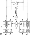
- FIG 3 shows a simplified diagram of a presently preferred clock recovery arrangement according to the invention.
- the analogue signal components xi, xq and yi, yq output by the 90°-hybrids ( FIG 1 ) are fed to analogue-digital converters 20, 21 of a first sample unit 15 and 24, 25 of a second sample unit 16.
- Sequences of the sampled component values XI, XQ and YI, YQ, (time variable [n] is here usually omitted) representing the signal components xi, xq, yi, yq, are fed to a combined phase error detector unit 17 to determine resulting phase error values X WPE , X RPE which are fed via a loop filter 18 as control signal CS - where required after digital-analogue conversion - to a controlled oscillator 19 (CO; numerical controlled or in the analogue domain voltage controlled) of a phase locked loop (PLL).
- the controlled oscillator 19 supplies the sampling units 15, 16 with a common clock signal CL or with separate clock signals.
- the clock signals may be adapted e.g. to different internal delay times.
- the inventive clock recovery can be used both with synchronous for analogue-digital embodiments and asynchronous sampling for full digital realisation.
- the sample frequency of the clock signal CL is a multiple of the symbol frequency for synchronous sampling, or slightly higher or lower if asynchronous sampling is used.
- the sampled values are re-sampled by interpolators 23, 24 and 26, 27 as known to those skilled in the art.
- the invention uses the combined phase error detector unit 17 for extracting the phase error signal from a plurality of linearly combined signal components.
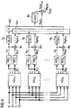
- the combined phase error detector unit 17 shown in FIG 4 comprises a set of N static equalizers EQU i with associated phase error detectors PED i .
- the component values XI, XQ and YI, YQ are fed parallel to all equalizers, each being optimized for a specific polarization mixing condition (polarisation mixing angle ⁇ ).
- polarisation mixing angle ⁇ polarisation mixing angle ⁇
- an optimized equalizer can reconstruct the transmitted orthogonal signals, in the shown embodiment represented by digital equalizer component values X Ei .
- each equalizer EQU i is fed to one of N phase error detectors PED i as well as to N gain coefficient estimators PCE i (PCE - derived from phase detector gain coefficients estimator).
- One of the equalizers may pass through at least one of the input component values, e.g. equalizer EQU 1 passes through component values XI, which are fed to a first phase error detector PED 1 instead of a modified equalizer output signal. But this "equalizer” may compensate other signal distortions.
- phase error detectors PED i output phase error values X PEi which are fed via multipliers M i to a first adder AD1, and the gain coefficient estimators PCE i output gain coefficients K i which are fed via squaring circuits Q i to a further adder AD3.
- the output of the first adder AD1 is connected to a normalizing multiplier M NOR and the output of the further adder AD3 is connected via a division device DD to a further input of said normalizing multiplier.
- the derived resultant weighted phase error values X WPE could be used as an input to the loop filter of the phase locked loop.
- the resulting phase error values X WPE become virtually independent of the input signal distortions by dividing them by a sum of squares of the individual gain coefficients K i summed up by the further adder AD3.
- the calculation of is executed by the division device DD.
- Multiplication with 1/ ⁇ Ki 2 and the scaling factor K SET is executed by the normalizing multiplier M NOR .
- the gain coefficient estimators PCE i - PCE N are the key for the preceding calculation, and hence for a robust clock recovery process. Therefore, a more detailed description of the gain coefficient estimation process will be given here.
- X Ei is at least one out of four signal components (XI Ei , XQ Ei , YI Ei , YQ Ei - only the outputs are shown in FIG 4 ) output from the i-th equalizer.
- Both signals X PEIi [n] and X PEQi [n], derived from equalizer output signals X Ei [n], are functions of the phase error and feature horizontal sinusoidal s-curves. Because they are in quadrature (like sine and cosine function), nearly phase-error-independent gain coefficients K i are obtained when they are "root mean squared" according to equation (4). Their amplitudes are functions of distortions and indicate the performances of the equalizers and are functions of the remaining distortions, mainly of DGD/T and ⁇ effects.
- the derived gain coefficients K i are almost independent of phase errors of the equalizers' output signals X Ei and indicate the quality of the phase information.
- the gain coefficients are used to calculate the resultant phase error values X RPE according to equation (3) which are almost independent of the distortions DGD/T and ⁇ of the component signals x and y.
- the arrangement may be upgraded by using both component values XI, XQ or YI, YQ for a complete Gardner phase error detector or even all component values. This is not shown in FIG 4 and not outlined in the formulas for clarity reasons.
- Two different PLLs may also be used for sampling the signal components xi, xq and yi, yq separately. Two resulting phase error values for the two PLLs are then generated separately by two different sets of phase detectors with allocated gain coefficient estimators.
- FIG 5 shows a further simplified low cost example of a clock recovery comprising two PLLs which does not form an embodiment of the present invention.
- the figure shows a simplified illustration of two sample units 15 and 16.
- a first and a second PLL are controlled by separate (Gardner) phase detector units 31 and 32.
- the first phase detector unit 31 controls via the loop filter 18 the controllable oscillator (CO) 19 generating a first sample signal CL1
- the second phase detector unit 32 controls via a second loop filter 32 a second CO 29 generating a second sample signal CL2.
- the x signal components xi, xq are sampled by the first sample signal CL1 and the y component signals yi, yq are sampled by second sample signal.
- the sampled XI and XQ component values are fed to a first phase error detector PD1, and the YI and YQ component values are fed to a second phase error detector PD2.
- a single fix equalizer 30 is used to generate two pairs of component values XI E , XQ E and YI E , YQ E rotated by 45° and fed to the additional phase detectors PD3 and PD4 respectively.
- the further phase error detectors PD3, PD4 generate appropriate phase error values X PE3 , Y PE4 according to their input values XI E , XQ E and YI E , YQ E respectively.
- Both phase error values X PE1 , X PE3 from the first and third phase error detector are fed to a first adder AD1 and combined to a first resulting phase error values X PE .
- Second resulting phase error values Y PE controlling the second loop are generated by the second phase error detector PD2 receiving the YI and YQ component values and by the fourth phase error detector PD4 receiving the component values XI E and XQ E from further equalizer outputs. Both phase error values Y PE2 and Y PE4 are added by the second adder AD2.
- FIG 6 shows the normalized gain coefficient K/K REF for the example shown in FIG 5 employing only one equalizer and trivial weighting of the phase detector outputs by the gain coefficients 1.0.
- the fluctuations of K/K REF versus DGD are relatively small.
- a second equalizer or further equalizers would improve the performance significantly.
- all static equalizers can be adjusted to compensate different distortions in order to achieve optimum performance.
Landscapes
- Engineering & Computer Science (AREA)
- Computer Networks & Wireless Communication (AREA)
- Signal Processing (AREA)
- Physics & Mathematics (AREA)
- Electromagnetism (AREA)
- Optics & Photonics (AREA)
- Synchronisation In Digital Transmission Systems (AREA)
- Digital Transmission Methods That Use Modulated Carrier Waves (AREA)
- Optical Communication System (AREA)
Claims (12)
- Takt-Wiedergewinnungsverfahren für kohärente Polarisationsmultiplex-Empfänger (1 - 14), das die folgenden Schritte umfasst:- kohärentes Demodulieren eines empfangenen Polarisationsmultiplex-Signals (PMS) und Ableiten orthogonaler Signalkomponenten (xi, xq; yi, yq),- Sampeln und Konvertieren der orthogonalen Signalkomponenten (xi, xq; yi, yq) in digitale Komponentenwerte (XI, XQ; YI, YQ), gekennzeichnet durch die folgenden Schritte:- paralleles Einführen der Komponentenwerte (xi, xq; yi, yq) in mehrere Equalizer (EQUi),- Ableiten von Phasenfehlerwerten (XPEi ; i = 1, 2, ..., N) aus Ausgabewerten (XEi; i = 1, 2, ..., N) der Equalizer (EQUi; i = 1, 2, ..., N),- Berechnen von resultierenden Phasenfehlerwerten (XWPE) aus mindestens zwei abgeleiteten Phasenfehlerwerten (XPEi ; i = 1, 2, ..., N),- Ableiten eines Oszillator-Steuersignals (CS) aus den resultierenden Phasenfehlerwerten (XWPE), und- Steuern mindestens eines steuerbaren Oszillators (19) zum Erzeugen eines Sample-Signals (CL) zum Sampeln der orthogonalen Signalkomponenten (xi, xq; yi, yq) oder zum Resampeln der Komponentenwerte.
- Takt-Wiedergewinnungsverfahren nach Anspruch 1, wobei einer der Equalizer (EQUi) mindestens einen der eingegebenen Komponentenwerte (XI, XQ; YI, YQ) unmodifiziert durchlässt.
- Takt-Wiedergewinnungsverfahren nach Anspruch 1 oder 2, umfassend einen Schritt, in dem resultierende Phasenfehlerwerte (XWPE, XRPE) berechnet werden, indem mehr als zwei Phasenfehlerwerte (XPEi; i = 1, 2, ..., N) kombiniert werden, die aus Ausgangswerten (XEi) von mehr als einem Equalizer (EQUi ; i = 1, 2, ..., N) abgeleitet sind.
- Takt-Wiedergewinnungsverfahren nach Anspruch 1, 2 oder 3, umfassend einen Schritt, in dem- Verstärkungskoeffizienten (Ki) als Gewichtungsfaktoren berechnet werden, die das Verhalten der Phasenfehlerdetektoren (PEDi) bewerten,- gewichtete Phasenfehlerwerte (XWPE) berechnet werden, indem die Verstärkungskoeffizienten (Ki) angewendet werden, und- die gewichteten Phasenfehlerwerte (XWPEi) addiert werden, um resultierende, gewichtete Phasenfehlerwerte (XWPE) abzuleiten.
- Takt-Wiedergewinnungsverfahren nach Anspruch 4, umfassend einen Schritt, in dem- quadrierte Verstärkungskoeffizienten (Ki 2) berechnet werden,- die quadrierten Verstärkungskoeffizienten (Ki 2) addiert werden,- ein Normalisierungsfaktor (1/∑Ki 2) abgeleitet wird, und- resultierende Phasenfehlerwerte (XWPE ; XRPE) berechnet werden, deren Amplituden im Wesentlichen unabhängig von einem Polarisationsmischungswinkel (α) zwischen empfangenen orthogonalen optischen Signalen und einem Polarisationsstrahlteiler (1), und von einer differenziellen Gruppenverzögerung (differential group delay, DGD) ist.
- Takt-Wiedergewinnungsverfahren nach Anspruch 4, umfassend einen Schritt, in dem- resultierende gewichtete Phasenfehlerwerte (XWPE) berechnet werden,



- Takt-Wiedergewinnungsverfahren nach Anspruch 5, umfassend einen Schritt, in dem- die Verstärkungskoeffizienten (Ki), die als Gewichtungsfaktoren verwendet werden, gemäß



- Takt-Wiedergewinnungsverfahren nach einem der folgenden Ansprüche, umfassend einen Schritt, in dem- Phasenfehlerwerte (XPEi ; YPEi) erzeugt werden, gemäß

- Takt-Wiedergewinnungsanordnung (10) für einen kohärenten Polarisationsmultiplexempfänger (1 - 14) mit mindestens einem Phasenregelkreis (phase locked loop) der ein Sample-Signal (CL) ableitet, umfassend eine Phasenfehler-Detektoreinheit (PED), die gesampelte Komponentenwerte (XI, XQ, YI, YQ) empfängt, einen Schleifenfilter (18; 28) und einen steuerbaren Oszillator (CO), umfassend- eine kombinierte Phasenfehler-Detektoreinheit (17) mit einer Mehrzahl von festen Equalizern (EQUi), die dazu geeignet sind, gesampelte Komponentenwerte (XI, XQ, YI, YQ) zu empfangen und Equalizerausgabewerte (XEi) auszugeben, mit- einer Mehrzahl von Phasenfehler-Detektoren (PEDi, i = 1, 2, ..., N ; PD1 - PD4), die geeignet sind, Equalizer - (EQUi) Ausgangswerte (XEi) zu empfangen und Phasenfehlerwerte (XPEi) zu erzeugen, und mit- Mitteln (AD1, AD2) zum Kombinieren von Phasenfehlersignalen (XPEi), um resultierende Fehlerwerte (XWPE, XRPE) abzuleiten, zum Steuern mindestens eines steuerbaren Oszillators (19) des mindestens einen Phasenregelkreises.
- Takt-Wiedergewinnungsanordnung nach Anspruch 9, wobei einer der Equalizer (EQUi) mindestens einen der eingegebenen Komponentenwerte (XI, XQ; YI, YQ) unmodifiziert durchlässt.
- Takt-Wiedergewinnungsanordnung nach Anspruch 10, umfassend- Verstärkungskoeffizientenschätzer (PCEi), die die Equalizer - (EQUi) Ausgangswerte (XEi ; XIE, XQE, YIE, YQE) empfangen, um Verstärkungskoeffizienten (Ki) als Gewichtungsfaktoren zu berechnen,- Multiplizierer (Mi), die Phasenfehlerwerte (XPEi) und zugehörige Verstärkungskoeffizienten (Ki) empfangen, um gewichtete Phasenfehlerwerte (XWPEi) zu berechnen,- einen ersten Addierer (AD1), der die gewichteten Phasenfehlerwerte (XWPEi) empfängt und resultierende gewichtete Phasenfehlerwerte (XWPE) berechnet, um den mindestens einen steuerbaren Oszillator (19) zu steuern.
- Takt-Wiedergewinnungsanordnung nach Anspruch 11, umfassend- Verstärkungskoeffizientenschätzer (PCEi), zum Ableiten von Verstärkungskoeffizienten (Ki), die das Verhalten der Phasenfehler-Detektoren (PEDi) repräsentieren,- Mittel (Qi, AD3, DD, MNOR) zum Ableiten resultierender Phasenfehlerwerte (XWPE, XRPE), die im Wesentlichen unabhängig von einem Polarisationsmischwinkel (α) zwischen empfangenen orthogonalen Signalen und einem Polarisationsstrahlteiler (1), und von einer differenziellen Gruppenverzögerung (differential group delay, DGD) sind.
Priority Applications (7)
| Application Number | Priority Date | Filing Date | Title |
|---|---|---|---|
| EP10001212.9A EP2375603B1 (de) | 2010-02-05 | 2010-02-05 | Taktwiederherstellungsverfahren und Taktwiederherstellungsanordung für Multiplex-Empfänger mit kohärenter Polarisation |
| PCT/EP2011/051441 WO2011095500A1 (en) | 2010-02-05 | 2011-02-02 | Clock recovery method and clock recovery arrangement for coherent polarisation multiplex receivers |
| US13/577,297 US9065590B2 (en) | 2010-02-05 | 2011-02-02 | Clock recovery method and clock recovery arrangement for coherent polarization multiplex receivers |
| CN201180008306.6A CN102725982B (zh) | 2010-02-05 | 2011-02-02 | 用于相干偏振复用接收机的时钟恢复方法及时钟恢复设备 |
| EP11702620.3A EP2532107B1 (de) | 2010-02-05 | 2011-02-02 | Taktwiederherstellungsverfahren und taktwiederherstellungsanordung für multiplex-empfänger mit kohärenter polarisation |
| US14/735,515 US9467246B2 (en) | 2010-02-05 | 2015-06-10 | Clock recovery method and clock recovery arrangement for coherent polarization multiplex receivers |
| US15/278,790 US9871615B2 (en) | 2010-02-05 | 2016-09-28 | Clock recovery method and clock recovery arrangement for coherent polarization multiplex receivers |
Applications Claiming Priority (1)
| Application Number | Priority Date | Filing Date | Title |
|---|---|---|---|
| EP10001212.9A EP2375603B1 (de) | 2010-02-05 | 2010-02-05 | Taktwiederherstellungsverfahren und Taktwiederherstellungsanordung für Multiplex-Empfänger mit kohärenter Polarisation |
Publications (2)
| Publication Number | Publication Date |
|---|---|
| EP2375603A1 EP2375603A1 (de) | 2011-10-12 |
| EP2375603B1 true EP2375603B1 (de) | 2018-05-23 |
Family
ID=42272240
Family Applications (2)
| Application Number | Title | Priority Date | Filing Date |
|---|---|---|---|
| EP10001212.9A Active EP2375603B1 (de) | 2010-02-05 | 2010-02-05 | Taktwiederherstellungsverfahren und Taktwiederherstellungsanordung für Multiplex-Empfänger mit kohärenter Polarisation |
| EP11702620.3A Active EP2532107B1 (de) | 2010-02-05 | 2011-02-02 | Taktwiederherstellungsverfahren und taktwiederherstellungsanordung für multiplex-empfänger mit kohärenter polarisation |
Family Applications After (1)
| Application Number | Title | Priority Date | Filing Date |
|---|---|---|---|
| EP11702620.3A Active EP2532107B1 (de) | 2010-02-05 | 2011-02-02 | Taktwiederherstellungsverfahren und taktwiederherstellungsanordung für multiplex-empfänger mit kohärenter polarisation |
Country Status (4)
| Country | Link |
|---|---|
| US (3) | US9065590B2 (de) |
| EP (2) | EP2375603B1 (de) |
| CN (1) | CN102725982B (de) |
| WO (1) | WO2011095500A1 (de) |
Families Citing this family (26)
| Publication number | Priority date | Publication date | Assignee | Title |
|---|---|---|---|---|
| JP5444877B2 (ja) * | 2009-06-24 | 2014-03-19 | 富士通株式会社 | デジタルコヒーレント受信器 |
| EP2375603B1 (de) | 2010-02-05 | 2018-05-23 | Xieon Networks S.à r.l. | Taktwiederherstellungsverfahren und Taktwiederherstellungsanordung für Multiplex-Empfänger mit kohärenter Polarisation |
| JP5733465B2 (ja) * | 2011-03-31 | 2015-06-10 | 富士通株式会社 | バタフライフィルタの係数設定方法とその装置、受信機、及び受信方法 |
| JP5720425B2 (ja) * | 2011-05-31 | 2015-05-20 | 富士通株式会社 | デジタルコヒーレント受信機及び位相制御方法 |
| US9584250B2 (en) * | 2011-12-30 | 2017-02-28 | Xieon Networks S.A.R.L. | Symbol timing estimation for coherent polarization multiplex optical receivers |
| US8737847B2 (en) * | 2012-03-19 | 2014-05-27 | Futurewei Technologies, Inc. | Method and apparatus of using joint timing recovery for a coherent optical system |
| CN103326722B (zh) * | 2012-03-19 | 2017-11-24 | 深圳市中兴微电子技术有限公司 | 一种自适应样值估计电路和方法 |
| WO2014194940A1 (en) * | 2013-06-05 | 2014-12-11 | Huawei Technologies Co., Ltd. | Coherent optical receiver |
| CN105612700B (zh) * | 2013-10-09 | 2017-12-29 | 华为技术有限公司 | 用于表征光接收信号的色度色散的装置 |
| CN104780037B (zh) * | 2014-01-10 | 2019-04-30 | 深圳市中兴微电子技术有限公司 | 一种时钟恢复方法、装置及系统 |
| US9608735B2 (en) * | 2014-03-11 | 2017-03-28 | Multiphy Ltd. | MIMO equalization optimized for baud rate clock recovery in coherent DP-QPSK metro systems |
| CN105791187B (zh) * | 2014-12-24 | 2019-04-30 | 深圳市中兴微电子技术有限公司 | 时钟恢复均衡装置与方法 |
| CN106716943B (zh) | 2015-05-12 | 2019-11-29 | 华为技术有限公司 | 一种符号同步方法及装置 |
| EP3316498B1 (de) | 2015-06-23 | 2021-08-11 | Huawei Technologies Co., Ltd. | Verfahren und vorrichtung zur phasenschätzung eines polarisationsmultiplexsystems |
| CN105245278B (zh) * | 2015-10-27 | 2017-08-25 | 广东省科技基础条件平台中心 | 一种可见光通信副载波复用时钟同步接收装置 |
| EP3220559A1 (de) * | 2016-03-14 | 2017-09-20 | Xieon Networks S.à r.l. | Parameterverarbeitung und gemeinsame ressourcennutzungsarchitektur für superkanalbasierte übertragungssysteme |
| US10128958B1 (en) * | 2016-10-24 | 2018-11-13 | Inphi Corporation | Forward and backward propagation methods and structures for coherent optical receiver |
| CN109218237B (zh) * | 2017-07-07 | 2021-02-19 | 扬智科技股份有限公司 | 实体层电路、时钟恢复电路与其频偏纠正方法 |
| CN110351066B (zh) * | 2018-04-02 | 2022-03-08 | 华为技术有限公司 | 时钟相位恢复装置、方法和芯片 |
| CN112640329B (zh) * | 2018-09-07 | 2025-01-03 | 日本电气株式会社 | 光学接收器和接收方法 |
| CN109302238B (zh) * | 2018-11-29 | 2020-08-14 | 武汉邮电科学研究院有限公司 | 一种光iq调制器参数调节方法及系统 |
| US10623174B1 (en) * | 2018-12-12 | 2020-04-14 | Xilinx, Inc. | Low latency data transfer technique for mesochronous divided clocks |
| CN112118063B (zh) * | 2019-06-21 | 2022-05-24 | 华为技术有限公司 | 一种时钟同步装置、光发射器、光接收器及方法 |
| US10985900B1 (en) * | 2020-03-03 | 2021-04-20 | Ciena Corporation | Estimating clock phase error based on channel conditions |
| WO2022199859A1 (en) * | 2021-03-22 | 2022-09-29 | Fundació Institut De Ciències Fotòniques | A method and a device for carrier recovery |
| US11962677B2 (en) | 2022-04-13 | 2024-04-16 | Stmicroelectronics S.R.L. | System and method for clock resynchronization |
Family Cites Families (55)
| Publication number | Priority date | Publication date | Assignee | Title |
|---|---|---|---|---|
| JP3403849B2 (ja) * | 1995-03-17 | 2003-05-06 | 富士通株式会社 | 多重無線装置の受信部に設けられるクロック位相検出回路及びクロック再生回路 |
| JP3414558B2 (ja) * | 1995-08-25 | 2003-06-09 | 沖電気工業株式会社 | 最大相関値タイミング推定回路及び受信装置 |
| US5805619A (en) * | 1996-02-16 | 1998-09-08 | Swan Magnetics, Inc. | Method and apparatus for sampled-data partial-response signal timing error detector having zero self-noise |
| US6330273B1 (en) * | 1996-03-28 | 2001-12-11 | Roke Manor Research Limited | Apparatus for code tracking in a direct sequence spread spectrum receiver |
| JPH1056487A (ja) * | 1996-08-09 | 1998-02-24 | Nec Corp | 直交復調回路 |
| KR100224837B1 (ko) * | 1997-02-21 | 1999-10-15 | 윤종용 | 디지털 vcr의 적응적인 신호 처리방법 및 그 회로 |
| US6304621B1 (en) * | 1998-05-13 | 2001-10-16 | Broadcom Corporation | Multi-mode variable rate digital cable receiver |
| US6370188B1 (en) * | 1999-03-31 | 2002-04-09 | Texas Instruments Incorporated | Phase and frequency offset compensation in a telecommunications receiver |
| US6560299B1 (en) * | 1999-07-30 | 2003-05-06 | Christopher H Strolle | Diversity receiver with joint signal processing |
| JP3419397B2 (ja) * | 2001-01-18 | 2003-06-23 | 日本電気株式会社 | クロック同期回路及びクロック同期方法 |
| US7010073B2 (en) * | 2001-01-19 | 2006-03-07 | Qualcomm, Incorporated | Delay lock loops for wireless communication systems |
| DE10133898C1 (de) * | 2001-07-12 | 2002-10-17 | Infineon Technologies Ag | Empfänger mit einem integrierten Taktphasendetektor |
| US7245658B2 (en) * | 2001-09-05 | 2007-07-17 | Mediatek, Inc. | Read channel apparatus for an optical storage system |
| US7062165B2 (en) * | 2001-12-26 | 2006-06-13 | Nortel Networks Limited | Receiver monitoring and optimization using forward error correction information |
| KR100493026B1 (ko) * | 2002-09-09 | 2005-06-07 | 삼성전자주식회사 | 전화선 모뎀을 위한 강건한 심벌 타이밍 복구 회로 |
| DE10243141B4 (de) * | 2002-09-17 | 2006-05-11 | Siemens Ag | Verfahren zur Übertragung von optischen Polarisationsmultiplexsignalen |
| US6922440B2 (en) * | 2002-12-17 | 2005-07-26 | Scintera Networks, Inc. | Adaptive signal latency control for communications systems signals |
| KR100510690B1 (ko) * | 2003-01-20 | 2005-08-31 | 엘지전자 주식회사 | 디지털 티브이 수신기 및 심볼 클럭 복구 장치 |
| US7200196B2 (en) * | 2003-04-24 | 2007-04-03 | Texas Instruments Incorporated | Interpolation based timing recovery |
| US20040223568A1 (en) * | 2003-05-09 | 2004-11-11 | Ming-Kang Liu | Phase sampling determination system |
| US20040223567A1 (en) * | 2003-05-09 | 2004-11-11 | Ming-Kang Liu | Clock recovery system |
| EP1531591A1 (de) * | 2003-11-11 | 2005-05-18 | STMicroelectronics Belgium N.V. | Abtastwerteauswahl für Zeitbereich-Interpolation |
| US7623797B2 (en) * | 2004-07-14 | 2009-11-24 | Fundacion Tarpuy | Compensating impairments of optical channel using adaptive equalization |
| DE602005024573D1 (de) * | 2004-08-30 | 2010-12-16 | Nec Corp | Taktregenerierungsschaltung |
| US7532822B2 (en) * | 2005-02-28 | 2009-05-12 | Nortel Networks Limited | Clock recovery from an optical signal with polarization impairments |
| US7555227B2 (en) * | 2005-10-21 | 2009-06-30 | Nortel Networks Limited | Polarization compensation in a coherent optical receiver |
| US7522841B2 (en) * | 2005-10-21 | 2009-04-21 | Nortel Networks Limited | Efficient data transmission and training of data processing functions |
| US7606498B1 (en) * | 2005-10-21 | 2009-10-20 | Nortel Networks Limited | Carrier recovery in a coherent optical receiver |
| US20080056403A1 (en) * | 2006-09-01 | 2008-03-06 | On Demand Microelectronics | Method and apparatus for timing recovery of pam signals |
| JP4186083B2 (ja) * | 2006-10-03 | 2008-11-26 | 日本電気株式会社 | クロック同期回路 |
| US8078065B2 (en) * | 2006-12-22 | 2011-12-13 | Alcatel Lucent | Polarization tracking and signal equalization for optical receivers configured for on-off keying or pulse amplitude modulation signaling |
| JP4303760B2 (ja) * | 2007-02-16 | 2009-07-29 | 富士通株式会社 | Ad変換制御装置、光受信装置および光受信方法 |
| US8036332B2 (en) * | 2007-03-30 | 2011-10-11 | 4472314 Canada Inc. | Communication signal symbol timing error detection and recovery |
| JP5034770B2 (ja) * | 2007-08-16 | 2012-09-26 | 富士通株式会社 | コヒーレント光受信器および光通信システム |
| US20090113504A1 (en) * | 2007-10-26 | 2009-04-30 | John Mezzalingua Associates, Inc. | Digital Signal Converter Device |
| US8005368B2 (en) * | 2007-12-05 | 2011-08-23 | Ciena Corporation | Signal equalizer in a coherent optical receiver |
| EP2086130B1 (de) * | 2008-01-29 | 2013-01-09 | Alcatel Lucent | Kombinierte Phasen- und Polarisationsmodulation für optische Kommunikationen |
| EP2086157B1 (de) * | 2008-01-30 | 2012-09-26 | Nokia Siemens Networks Oy | Verfahren und Vorrichtung zur Verarbeitung von Daten und Kommunikationssystem mit einer derartigen Vorrichtung |
| EP2109272B1 (de) * | 2008-04-10 | 2018-10-31 | Xieon Networks S.à r.l. | Verfahren und Vorrichtung zur Phasenrückgewinnung und Kommunikationssystem mit einer derartigen Vorrichtung |
| CN101599801B (zh) * | 2008-06-06 | 2012-02-22 | 富士通株式会社 | 滤波器系数调整装置和方法 |
| CN101599929B (zh) | 2008-06-06 | 2012-11-21 | 富士通株式会社 | 自适应均衡装置和方法 |
| JP5136236B2 (ja) * | 2008-06-19 | 2013-02-06 | 富士通株式会社 | 光受信装置 |
| JP5359179B2 (ja) * | 2008-10-17 | 2013-12-04 | 富士通株式会社 | 光受信機及び光受信方法 |
| US8798122B2 (en) * | 2008-12-09 | 2014-08-05 | Telefonaktiebolaget L M Ericsson (Publ) | Symbol-timing recovery techniques for multi-branch receivers |
| US8135283B2 (en) * | 2009-04-07 | 2012-03-13 | Ciena Corporation | Clock recovery with channel coefficients |
| JP5024481B2 (ja) * | 2009-05-07 | 2012-09-12 | 日本電気株式会社 | コヒーレント受信機 |
| US8861648B2 (en) * | 2009-05-11 | 2014-10-14 | Nec Corporation | Receiving device and demodulation device |
| US8655191B2 (en) * | 2009-06-29 | 2014-02-18 | Alcatel Lucent | Symbol timing recovery in polarization division multiplexed coherent optical transmission system |
| KR20110005575A (ko) * | 2009-07-10 | 2011-01-18 | 한국전자통신연구원 | 코히어런트 광 수신기의 디지털 등화 장치 및 방법 |
| US8331803B2 (en) * | 2009-10-07 | 2012-12-11 | Futurewei Technologies, Inc. | Clock recovery method for polarization multiplexed coherent optical communications |
| US8244142B2 (en) * | 2009-10-28 | 2012-08-14 | Opnext Subsystems, Inc. | Optical receiver having fractional sampling |
| US8761609B1 (en) * | 2009-11-02 | 2014-06-24 | Clariphy Communications, Inc. | High-speed optical communications system |
| US8737542B1 (en) * | 2010-01-12 | 2014-05-27 | Marvell International Ltd. | Method and apparatus for data reception in high-speed applications |
| EP2375603B1 (de) | 2010-02-05 | 2018-05-23 | Xieon Networks S.à r.l. | Taktwiederherstellungsverfahren und Taktwiederherstellungsanordung für Multiplex-Empfänger mit kohärenter Polarisation |
| JP5482273B2 (ja) * | 2010-02-12 | 2014-05-07 | 富士通株式会社 | 光受信器 |
-
2010
- 2010-02-05 EP EP10001212.9A patent/EP2375603B1/de active Active
-
2011
- 2011-02-02 WO PCT/EP2011/051441 patent/WO2011095500A1/en not_active Ceased
- 2011-02-02 EP EP11702620.3A patent/EP2532107B1/de active Active
- 2011-02-02 CN CN201180008306.6A patent/CN102725982B/zh active Active
- 2011-02-02 US US13/577,297 patent/US9065590B2/en active Active
-
2015
- 2015-06-10 US US14/735,515 patent/US9467246B2/en active Active
-
2016
- 2016-09-28 US US15/278,790 patent/US9871615B2/en active Active
Non-Patent Citations (1)
| Title |
|---|
| None * |
Also Published As
| Publication number | Publication date |
|---|---|
| US20170019206A1 (en) | 2017-01-19 |
| EP2532107A1 (de) | 2012-12-12 |
| US20150280857A1 (en) | 2015-10-01 |
| US9065590B2 (en) | 2015-06-23 |
| EP2532107B1 (de) | 2017-05-17 |
| CN102725982B (zh) | 2016-08-03 |
| CN102725982A (zh) | 2012-10-10 |
| US9871615B2 (en) | 2018-01-16 |
| WO2011095500A1 (en) | 2011-08-11 |
| US9467246B2 (en) | 2016-10-11 |
| EP2375603A1 (de) | 2011-10-12 |
| US20120308234A1 (en) | 2012-12-06 |
Similar Documents
| Publication | Publication Date | Title |
|---|---|---|
| EP2375603B1 (de) | Taktwiederherstellungsverfahren und Taktwiederherstellungsanordung für Multiplex-Empfänger mit kohärenter Polarisation | |
| US7555227B2 (en) | Polarization compensation in a coherent optical receiver | |
| JP5407595B2 (ja) | 信号処理回路、光受信装置、検出装置および波形歪補償方法 | |
| US8655191B2 (en) | Symbol timing recovery in polarization division multiplexed coherent optical transmission system | |
| US8571423B2 (en) | Receiver algorithms for coherent detection of polarization-multiplexed optical signals | |
| US8526831B2 (en) | Receiver algorithms for coherent detection of polarization-multiplexed optical signals | |
| US9240843B1 (en) | Method and apparatus for blind time skew compensation for coherent optical receivers | |
| EP3932029B1 (de) | Taktphasenerkennung durch benutzung innerer spektraler komponenten | |
| EP2798766B1 (de) | Symbolzeitabschätzung für optische multiplex empfänger mit kohärenter polarisation | |
| EP3926860B1 (de) | Trainingsgestützte vorwärtsgerichtete kanalentzerrung | |
| US20120148265A1 (en) | Coherent optical receiving device capable of digital equalization of optical input, digital equalization method for optical input and coherent optical transmitting/receiving device | |
| EP2436128A1 (de) | Vorrichtung zur wiederherstellung von taktphasen | |
| WO2014194940A1 (en) | Coherent optical receiver | |
| Sun et al. | Timing synchronization in coherent optical transmission systems | |
| WO2013174304A1 (en) | Method with improved phase robustness in coherent detected optical system | |
| Zou et al. | FPGA Implementation of Parallel Non-Integer Oversampling Timing Recovery with IQ Skew Compensation | |
| EP2976852B1 (de) | Taktrückgewinnungsvorrichtung | |
| JP2025079661A (ja) | 光受信装置及び光伝送システム | |
| BR102016018326B1 (pt) | Sistema e método de recuperação de relógio em receptores ópticos coerentes com fatiamento espectral e reconstrução de sinal por equalizador mimo |
Legal Events
| Date | Code | Title | Description |
|---|---|---|---|
| PUAI | Public reference made under article 153(3) epc to a published international application that has entered the european phase |
Free format text: ORIGINAL CODE: 0009012 |
|
| AK | Designated contracting states |
Kind code of ref document: A1 Designated state(s): AT BE BG CH CY CZ DE DK EE ES FI FR GB GR HR HU IE IS IT LI LT LU LV MC MK MT NL NO PL PT RO SE SI SK SM TR |
|
| AX | Request for extension of the european patent |
Extension state: AL BA RS |
|
| 17P | Request for examination filed |
Effective date: 20120412 |
|
| 17Q | First examination report despatched |
Effective date: 20130307 |
|
| RAP1 | Party data changed (applicant data changed or rights of an application transferred) |
Owner name: NOKIA SOLUTIONS AND NETWORKS GMBH & CO. KG |
|
| RAP1 | Party data changed (applicant data changed or rights of an application transferred) |
Owner name: XIEON NETWORKS S.A.R.L. |
|
| RAP1 | Party data changed (applicant data changed or rights of an application transferred) |
Owner name: XIEON NETWORKS S.A R.L. |
|
| STAA | Information on the status of an ep patent application or granted ep patent |
Free format text: STATUS: EXAMINATION IS IN PROGRESS |
|
| REG | Reference to a national code |
Ref country code: DE Ref legal event code: R079 Ref document number: 602010050730 Country of ref document: DE Free format text: PREVIOUS MAIN CLASS: H04J0014060000 Ipc: H04B0010610000 |
|
| GRAP | Despatch of communication of intention to grant a patent |
Free format text: ORIGINAL CODE: EPIDOSNIGR1 |
|
| STAA | Information on the status of an ep patent application or granted ep patent |
Free format text: STATUS: GRANT OF PATENT IS INTENDED |
|
| RIC1 | Information provided on ipc code assigned before grant |
Ipc: H04L 7/00 20060101ALI20171114BHEP Ipc: H04L 7/033 20060101ALI20171114BHEP Ipc: H04J 14/06 20060101ALI20171114BHEP Ipc: H04B 10/61 20130101AFI20171114BHEP |
|
| INTG | Intention to grant announced |
Effective date: 20171211 |
|
| GRAS | Grant fee paid |
Free format text: ORIGINAL CODE: EPIDOSNIGR3 |
|
| GRAA | (expected) grant |
Free format text: ORIGINAL CODE: 0009210 |
|
| STAA | Information on the status of an ep patent application or granted ep patent |
Free format text: STATUS: THE PATENT HAS BEEN GRANTED |
|
| AK | Designated contracting states |
Kind code of ref document: B1 Designated state(s): AT BE BG CH CY CZ DE DK EE ES FI FR GB GR HR HU IE IS IT LI LT LU LV MC MK MT NL NO PL PT RO SE SI SK SM TR |
|
| REG | Reference to a national code |
Ref country code: GB Ref legal event code: FG4D |
|
| REG | Reference to a national code |
Ref country code: CH Ref legal event code: EP |
|
| REG | Reference to a national code |
Ref country code: IE Ref legal event code: FG4D |
|
| REG | Reference to a national code |
Ref country code: AT Ref legal event code: REF Ref document number: 1002367 Country of ref document: AT Kind code of ref document: T Effective date: 20180615 |
|
| REG | Reference to a national code |
Ref country code: DE Ref legal event code: R096 Ref document number: 602010050730 Country of ref document: DE |
|
| REG | Reference to a national code |
Ref country code: NL Ref legal event code: MP Effective date: 20180523 |
|
| REG | Reference to a national code |
Ref country code: LT Ref legal event code: MG4D |
|
| PG25 | Lapsed in a contracting state [announced via postgrant information from national office to epo] |
Ref country code: ES Free format text: LAPSE BECAUSE OF FAILURE TO SUBMIT A TRANSLATION OF THE DESCRIPTION OR TO PAY THE FEE WITHIN THE PRESCRIBED TIME-LIMIT Effective date: 20180523 Ref country code: NO Free format text: LAPSE BECAUSE OF FAILURE TO SUBMIT A TRANSLATION OF THE DESCRIPTION OR TO PAY THE FEE WITHIN THE PRESCRIBED TIME-LIMIT Effective date: 20180823 Ref country code: FI Free format text: LAPSE BECAUSE OF FAILURE TO SUBMIT A TRANSLATION OF THE DESCRIPTION OR TO PAY THE FEE WITHIN THE PRESCRIBED TIME-LIMIT Effective date: 20180523 Ref country code: LT Free format text: LAPSE BECAUSE OF FAILURE TO SUBMIT A TRANSLATION OF THE DESCRIPTION OR TO PAY THE FEE WITHIN THE PRESCRIBED TIME-LIMIT Effective date: 20180523 Ref country code: BG Free format text: LAPSE BECAUSE OF FAILURE TO SUBMIT A TRANSLATION OF THE DESCRIPTION OR TO PAY THE FEE WITHIN THE PRESCRIBED TIME-LIMIT Effective date: 20180823 Ref country code: SE Free format text: LAPSE BECAUSE OF FAILURE TO SUBMIT A TRANSLATION OF THE DESCRIPTION OR TO PAY THE FEE WITHIN THE PRESCRIBED TIME-LIMIT Effective date: 20180523 |
|
| PG25 | Lapsed in a contracting state [announced via postgrant information from national office to epo] |
Ref country code: GR Free format text: LAPSE BECAUSE OF FAILURE TO SUBMIT A TRANSLATION OF THE DESCRIPTION OR TO PAY THE FEE WITHIN THE PRESCRIBED TIME-LIMIT Effective date: 20180824 Ref country code: HR Free format text: LAPSE BECAUSE OF FAILURE TO SUBMIT A TRANSLATION OF THE DESCRIPTION OR TO PAY THE FEE WITHIN THE PRESCRIBED TIME-LIMIT Effective date: 20180523 Ref country code: LV Free format text: LAPSE BECAUSE OF FAILURE TO SUBMIT A TRANSLATION OF THE DESCRIPTION OR TO PAY THE FEE WITHIN THE PRESCRIBED TIME-LIMIT Effective date: 20180523 Ref country code: NL Free format text: LAPSE BECAUSE OF FAILURE TO SUBMIT A TRANSLATION OF THE DESCRIPTION OR TO PAY THE FEE WITHIN THE PRESCRIBED TIME-LIMIT Effective date: 20180523 |
|
| REG | Reference to a national code |
Ref country code: CH Ref legal event code: PK Free format text: BERICHTIGUNGEN |
|
| REG | Reference to a national code |
Ref country code: AT Ref legal event code: MK05 Ref document number: 1002367 Country of ref document: AT Kind code of ref document: T Effective date: 20180523 |
|
| RIC2 | Information provided on ipc code assigned after grant |
Ipc: H04L 7/00 20060101ALI20171114BHEP Ipc: H04J 14/06 20060101ALI20171114BHEP Ipc: H04B 10/61 20130101AFI20171114BHEP Ipc: H04L 7/033 20060101ALI20171114BHEP |
|
| PG25 | Lapsed in a contracting state [announced via postgrant information from national office to epo] |
Ref country code: CZ Free format text: LAPSE BECAUSE OF FAILURE TO SUBMIT A TRANSLATION OF THE DESCRIPTION OR TO PAY THE FEE WITHIN THE PRESCRIBED TIME-LIMIT Effective date: 20180523 Ref country code: SK Free format text: LAPSE BECAUSE OF FAILURE TO SUBMIT A TRANSLATION OF THE DESCRIPTION OR TO PAY THE FEE WITHIN THE PRESCRIBED TIME-LIMIT Effective date: 20180523 Ref country code: RO Free format text: LAPSE BECAUSE OF FAILURE TO SUBMIT A TRANSLATION OF THE DESCRIPTION OR TO PAY THE FEE WITHIN THE PRESCRIBED TIME-LIMIT Effective date: 20180523 Ref country code: PL Free format text: LAPSE BECAUSE OF FAILURE TO SUBMIT A TRANSLATION OF THE DESCRIPTION OR TO PAY THE FEE WITHIN THE PRESCRIBED TIME-LIMIT Effective date: 20180523 Ref country code: DK Free format text: LAPSE BECAUSE OF FAILURE TO SUBMIT A TRANSLATION OF THE DESCRIPTION OR TO PAY THE FEE WITHIN THE PRESCRIBED TIME-LIMIT Effective date: 20180523 Ref country code: EE Free format text: LAPSE BECAUSE OF FAILURE TO SUBMIT A TRANSLATION OF THE DESCRIPTION OR TO PAY THE FEE WITHIN THE PRESCRIBED TIME-LIMIT Effective date: 20180523 Ref country code: AT Free format text: LAPSE BECAUSE OF FAILURE TO SUBMIT A TRANSLATION OF THE DESCRIPTION OR TO PAY THE FEE WITHIN THE PRESCRIBED TIME-LIMIT Effective date: 20180523 |
|
| REG | Reference to a national code |
Ref country code: CH Ref legal event code: PK Free format text: BERICHTIGUNGEN |
|
| RIC2 | Information provided on ipc code assigned after grant |
Ipc: H04L 7/033 20060101ALI20171114BHEP Ipc: H04J 14/06 20060101ALI20171114BHEP Ipc: H04B 10/61 20130101AFI20171114BHEP Ipc: H04L 7/00 20060101ALI20171114BHEP |
|
| REG | Reference to a national code |
Ref country code: DE Ref legal event code: R097 Ref document number: 602010050730 Country of ref document: DE |
|
| PG25 | Lapsed in a contracting state [announced via postgrant information from national office to epo] |
Ref country code: IT Free format text: LAPSE BECAUSE OF FAILURE TO SUBMIT A TRANSLATION OF THE DESCRIPTION OR TO PAY THE FEE WITHIN THE PRESCRIBED TIME-LIMIT Effective date: 20180523 Ref country code: SM Free format text: LAPSE BECAUSE OF FAILURE TO SUBMIT A TRANSLATION OF THE DESCRIPTION OR TO PAY THE FEE WITHIN THE PRESCRIBED TIME-LIMIT Effective date: 20180523 |
|
| PLBE | No opposition filed within time limit |
Free format text: ORIGINAL CODE: 0009261 |
|
| STAA | Information on the status of an ep patent application or granted ep patent |
Free format text: STATUS: NO OPPOSITION FILED WITHIN TIME LIMIT |
|
| 26N | No opposition filed |
Effective date: 20190226 |
|
| PG25 | Lapsed in a contracting state [announced via postgrant information from national office to epo] |
Ref country code: SI Free format text: LAPSE BECAUSE OF FAILURE TO SUBMIT A TRANSLATION OF THE DESCRIPTION OR TO PAY THE FEE WITHIN THE PRESCRIBED TIME-LIMIT Effective date: 20180523 |
|
| REG | Reference to a national code |
Ref country code: CH Ref legal event code: PL |
|
| GBPC | Gb: european patent ceased through non-payment of renewal fee |
Effective date: 20190205 |
|
| PG25 | Lapsed in a contracting state [announced via postgrant information from national office to epo] |
Ref country code: MC Free format text: LAPSE BECAUSE OF FAILURE TO SUBMIT A TRANSLATION OF THE DESCRIPTION OR TO PAY THE FEE WITHIN THE PRESCRIBED TIME-LIMIT Effective date: 20180523 Ref country code: LU Free format text: LAPSE BECAUSE OF NON-PAYMENT OF DUE FEES Effective date: 20190205 |
|
| REG | Reference to a national code |
Ref country code: BE Ref legal event code: MM Effective date: 20190228 |
|
| REG | Reference to a national code |
Ref country code: IE Ref legal event code: MM4A |
|
| PG25 | Lapsed in a contracting state [announced via postgrant information from national office to epo] |
Ref country code: LI Free format text: LAPSE BECAUSE OF NON-PAYMENT OF DUE FEES Effective date: 20190228 Ref country code: CH Free format text: LAPSE BECAUSE OF NON-PAYMENT OF DUE FEES Effective date: 20190228 |
|
| PG25 | Lapsed in a contracting state [announced via postgrant information from national office to epo] |
Ref country code: IE Free format text: LAPSE BECAUSE OF NON-PAYMENT OF DUE FEES Effective date: 20190205 Ref country code: GB Free format text: LAPSE BECAUSE OF NON-PAYMENT OF DUE FEES Effective date: 20190205 |
|
| PG25 | Lapsed in a contracting state [announced via postgrant information from national office to epo] |
Ref country code: BE Free format text: LAPSE BECAUSE OF NON-PAYMENT OF DUE FEES Effective date: 20190228 |
|
| PG25 | Lapsed in a contracting state [announced via postgrant information from national office to epo] |
Ref country code: TR Free format text: LAPSE BECAUSE OF FAILURE TO SUBMIT A TRANSLATION OF THE DESCRIPTION OR TO PAY THE FEE WITHIN THE PRESCRIBED TIME-LIMIT Effective date: 20180523 |
|
| PG25 | Lapsed in a contracting state [announced via postgrant information from national office to epo] |
Ref country code: PT Free format text: LAPSE BECAUSE OF FAILURE TO SUBMIT A TRANSLATION OF THE DESCRIPTION OR TO PAY THE FEE WITHIN THE PRESCRIBED TIME-LIMIT Effective date: 20180924 Ref country code: MT Free format text: LAPSE BECAUSE OF NON-PAYMENT OF DUE FEES Effective date: 20190205 |
|
| PGFP | Annual fee paid to national office [announced via postgrant information from national office to epo] |
Ref country code: FR Payment date: 20200219 Year of fee payment: 11 |
|
| PG25 | Lapsed in a contracting state [announced via postgrant information from national office to epo] |
Ref country code: CY Free format text: LAPSE BECAUSE OF FAILURE TO SUBMIT A TRANSLATION OF THE DESCRIPTION OR TO PAY THE FEE WITHIN THE PRESCRIBED TIME-LIMIT Effective date: 20180523 |
|
| PG25 | Lapsed in a contracting state [announced via postgrant information from national office to epo] |
Ref country code: IS Free format text: LAPSE BECAUSE OF FAILURE TO SUBMIT A TRANSLATION OF THE DESCRIPTION OR TO PAY THE FEE WITHIN THE PRESCRIBED TIME-LIMIT Effective date: 20180923 |
|
| PG25 | Lapsed in a contracting state [announced via postgrant information from national office to epo] |
Ref country code: HU Free format text: LAPSE BECAUSE OF FAILURE TO SUBMIT A TRANSLATION OF THE DESCRIPTION OR TO PAY THE FEE WITHIN THE PRESCRIBED TIME-LIMIT; INVALID AB INITIO Effective date: 20100205 |
|
| PG25 | Lapsed in a contracting state [announced via postgrant information from national office to epo] |
Ref country code: FR Free format text: LAPSE BECAUSE OF NON-PAYMENT OF DUE FEES Effective date: 20210228 |
|
| PG25 | Lapsed in a contracting state [announced via postgrant information from national office to epo] |
Ref country code: MK Free format text: LAPSE BECAUSE OF FAILURE TO SUBMIT A TRANSLATION OF THE DESCRIPTION OR TO PAY THE FEE WITHIN THE PRESCRIBED TIME-LIMIT Effective date: 20180523 |
|
| PGFP | Annual fee paid to national office [announced via postgrant information from national office to epo] |
Ref country code: DE Payment date: 20251230 Year of fee payment: 17 |