EP2376434B1 - Matériau fonctionnel destiné à des composants électroniques imprimés - Google Patents
Matériau fonctionnel destiné à des composants électroniques imprimés Download PDFInfo
- Publication number
- EP2376434B1 EP2376434B1 EP09799248.1A EP09799248A EP2376434B1 EP 2376434 B1 EP2376434 B1 EP 2376434B1 EP 09799248 A EP09799248 A EP 09799248A EP 2376434 B1 EP2376434 B1 EP 2376434B1
- Authority
- EP
- European Patent Office
- Prior art keywords
- oxide
- indium
- gallium
- hafnium
- magnesium
- Prior art date
- Legal status (The legal status is an assumption and is not a legal conclusion. Google has not performed a legal analysis and makes no representation as to the accuracy of the status listed.)
- Not-in-force
Links
Images


Classifications
-
- C—CHEMISTRY; METALLURGY
- C07—ORGANIC CHEMISTRY
- C07F—ACYCLIC, CARBOCYCLIC OR HETEROCYCLIC COMPOUNDS CONTAINING ELEMENTS OTHER THAN CARBON, HYDROGEN, HALOGEN, OXYGEN, NITROGEN, SULFUR, SELENIUM OR TELLURIUM
- C07F3/00—Compounds containing elements of Groups 2 or 12 of the Periodic Table
- C07F3/02—Magnesium compounds
-
- C—CHEMISTRY; METALLURGY
- C09—DYES; PAINTS; POLISHES; NATURAL RESINS; ADHESIVES; COMPOSITIONS NOT OTHERWISE PROVIDED FOR; APPLICATIONS OF MATERIALS NOT OTHERWISE PROVIDED FOR
- C09D—COATING COMPOSITIONS, e.g. PAINTS, VARNISHES OR LACQUERS; FILLING PASTES; CHEMICAL PAINT OR INK REMOVERS; INKS; CORRECTING FLUIDS; WOODSTAINS; PASTES OR SOLIDS FOR COLOURING OR PRINTING; USE OF MATERIALS THEREFOR
- C09D11/00—Inks
- C09D11/02—Printing inks
-
- H—ELECTRICITY
- H10—SEMICONDUCTOR DEVICES; ELECTRIC SOLID-STATE DEVICES NOT OTHERWISE PROVIDED FOR
- H10D—INORGANIC ELECTRIC SEMICONDUCTOR DEVICES
- H10D30/00—Field-effect transistors [FET]
- H10D30/60—Insulated-gate field-effect transistors [IGFET]
- H10D30/67—Thin-film transistors [TFT]
-
- C—CHEMISTRY; METALLURGY
- C07—ORGANIC CHEMISTRY
- C07C—ACYCLIC OR CARBOCYCLIC COMPOUNDS
- C07C249/00—Preparation of compounds containing nitrogen atoms doubly-bound to a carbon skeleton
- C07C249/04—Preparation of compounds containing nitrogen atoms doubly-bound to a carbon skeleton of oximes
- C07C249/08—Preparation of compounds containing nitrogen atoms doubly-bound to a carbon skeleton of oximes by reaction of hydroxylamines with carbonyl compounds
-
- C—CHEMISTRY; METALLURGY
- C07—ORGANIC CHEMISTRY
- C07C—ACYCLIC OR CARBOCYCLIC COMPOUNDS
- C07C251/00—Compounds containing nitrogen atoms doubly-bound to a carbon skeleton
- C07C251/32—Oximes
- C07C251/70—Metal complexes of oximes
-
- C—CHEMISTRY; METALLURGY
- C07—ORGANIC CHEMISTRY
- C07F—ACYCLIC, CARBOCYCLIC OR HETEROCYCLIC COMPOUNDS CONTAINING ELEMENTS OTHER THAN CARBON, HYDROGEN, HALOGEN, OXYGEN, NITROGEN, SULFUR, SELENIUM OR TELLURIUM
- C07F7/00—Compounds containing elements of Groups 4 or 14 of the Periodic Table
- C07F7/22—Tin compounds
- C07F7/2204—Not belonging to the groups C07F7/2208 - C07F7/2296
-
- C—CHEMISTRY; METALLURGY
- C09—DYES; PAINTS; POLISHES; NATURAL RESINS; ADHESIVES; COMPOSITIONS NOT OTHERWISE PROVIDED FOR; APPLICATIONS OF MATERIALS NOT OTHERWISE PROVIDED FOR
- C09D—COATING COMPOSITIONS, e.g. PAINTS, VARNISHES OR LACQUERS; FILLING PASTES; CHEMICAL PAINT OR INK REMOVERS; INKS; CORRECTING FLUIDS; WOODSTAINS; PASTES OR SOLIDS FOR COLOURING OR PRINTING; USE OF MATERIALS THEREFOR
- C09D11/00—Inks
- C09D11/02—Printing inks
- C09D11/03—Printing inks characterised by features other than the chemical nature of the binder
-
- C—CHEMISTRY; METALLURGY
- C09—DYES; PAINTS; POLISHES; NATURAL RESINS; ADHESIVES; COMPOSITIONS NOT OTHERWISE PROVIDED FOR; APPLICATIONS OF MATERIALS NOT OTHERWISE PROVIDED FOR
- C09D—COATING COMPOSITIONS, e.g. PAINTS, VARNISHES OR LACQUERS; FILLING PASTES; CHEMICAL PAINT OR INK REMOVERS; INKS; CORRECTING FLUIDS; WOODSTAINS; PASTES OR SOLIDS FOR COLOURING OR PRINTING; USE OF MATERIALS THEREFOR
- C09D11/00—Inks
- C09D11/30—Inkjet printing inks
- C09D11/38—Inkjet printing inks characterised by non-macromolecular additives other than solvents, pigments or dyes
-
- C—CHEMISTRY; METALLURGY
- C09—DYES; PAINTS; POLISHES; NATURAL RESINS; ADHESIVES; COMPOSITIONS NOT OTHERWISE PROVIDED FOR; APPLICATIONS OF MATERIALS NOT OTHERWISE PROVIDED FOR
- C09D—COATING COMPOSITIONS, e.g. PAINTS, VARNISHES OR LACQUERS; FILLING PASTES; CHEMICAL PAINT OR INK REMOVERS; INKS; CORRECTING FLUIDS; WOODSTAINS; PASTES OR SOLIDS FOR COLOURING OR PRINTING; USE OF MATERIALS THEREFOR
- C09D11/00—Inks
- C09D11/52—Electrically conductive inks
-
- C—CHEMISTRY; METALLURGY
- C23—COATING METALLIC MATERIAL; COATING MATERIAL WITH METALLIC MATERIAL; CHEMICAL SURFACE TREATMENT; DIFFUSION TREATMENT OF METALLIC MATERIAL; COATING BY VACUUM EVAPORATION, BY SPUTTERING, BY ION IMPLANTATION OR BY CHEMICAL VAPOUR DEPOSITION, IN GENERAL; INHIBITING CORROSION OF METALLIC MATERIAL OR INCRUSTATION IN GENERAL
- C23C—COATING METALLIC MATERIAL; COATING MATERIAL WITH METALLIC MATERIAL; SURFACE TREATMENT OF METALLIC MATERIAL BY DIFFUSION INTO THE SURFACE, BY CHEMICAL CONVERSION OR SUBSTITUTION; COATING BY VACUUM EVAPORATION, BY SPUTTERING, BY ION IMPLANTATION OR BY CHEMICAL VAPOUR DEPOSITION, IN GENERAL
- C23C18/00—Chemical coating by decomposition of either liquid compounds or solutions of the coating forming compounds, without leaving reaction products of surface material in the coating; Contact plating
- C23C18/02—Chemical coating by decomposition of either liquid compounds or solutions of the coating forming compounds, without leaving reaction products of surface material in the coating; Contact plating by thermal decomposition
- C23C18/12—Chemical coating by decomposition of either liquid compounds or solutions of the coating forming compounds, without leaving reaction products of surface material in the coating; Contact plating by thermal decomposition characterised by the deposition of inorganic material other than metallic material
- C23C18/1204—Chemical coating by decomposition of either liquid compounds or solutions of the coating forming compounds, without leaving reaction products of surface material in the coating; Contact plating by thermal decomposition characterised by the deposition of inorganic material other than metallic material inorganic material, e.g. non-oxide and non-metallic such as sulfides, nitrides based compounds
- C23C18/1208—Oxides, e.g. ceramics
- C23C18/1216—Metal oxides
-
- C—CHEMISTRY; METALLURGY
- C23—COATING METALLIC MATERIAL; COATING MATERIAL WITH METALLIC MATERIAL; CHEMICAL SURFACE TREATMENT; DIFFUSION TREATMENT OF METALLIC MATERIAL; COATING BY VACUUM EVAPORATION, BY SPUTTERING, BY ION IMPLANTATION OR BY CHEMICAL VAPOUR DEPOSITION, IN GENERAL; INHIBITING CORROSION OF METALLIC MATERIAL OR INCRUSTATION IN GENERAL
- C23C—COATING METALLIC MATERIAL; COATING MATERIAL WITH METALLIC MATERIAL; SURFACE TREATMENT OF METALLIC MATERIAL BY DIFFUSION INTO THE SURFACE, BY CHEMICAL CONVERSION OR SUBSTITUTION; COATING BY VACUUM EVAPORATION, BY SPUTTERING, BY ION IMPLANTATION OR BY CHEMICAL VAPOUR DEPOSITION, IN GENERAL
- C23C18/00—Chemical coating by decomposition of either liquid compounds or solutions of the coating forming compounds, without leaving reaction products of surface material in the coating; Contact plating
- C23C18/02—Chemical coating by decomposition of either liquid compounds or solutions of the coating forming compounds, without leaving reaction products of surface material in the coating; Contact plating by thermal decomposition
- C23C18/12—Chemical coating by decomposition of either liquid compounds or solutions of the coating forming compounds, without leaving reaction products of surface material in the coating; Contact plating by thermal decomposition characterised by the deposition of inorganic material other than metallic material
- C23C18/125—Process of deposition of the inorganic material
- C23C18/1279—Process of deposition of the inorganic material performed under reactive atmosphere, e.g. oxidising or reducing atmospheres
-
- C—CHEMISTRY; METALLURGY
- C23—COATING METALLIC MATERIAL; COATING MATERIAL WITH METALLIC MATERIAL; CHEMICAL SURFACE TREATMENT; DIFFUSION TREATMENT OF METALLIC MATERIAL; COATING BY VACUUM EVAPORATION, BY SPUTTERING, BY ION IMPLANTATION OR BY CHEMICAL VAPOUR DEPOSITION, IN GENERAL; INHIBITING CORROSION OF METALLIC MATERIAL OR INCRUSTATION IN GENERAL
- C23C—COATING METALLIC MATERIAL; COATING MATERIAL WITH METALLIC MATERIAL; SURFACE TREATMENT OF METALLIC MATERIAL BY DIFFUSION INTO THE SURFACE, BY CHEMICAL CONVERSION OR SUBSTITUTION; COATING BY VACUUM EVAPORATION, BY SPUTTERING, BY ION IMPLANTATION OR BY CHEMICAL VAPOUR DEPOSITION, IN GENERAL
- C23C18/00—Chemical coating by decomposition of either liquid compounds or solutions of the coating forming compounds, without leaving reaction products of surface material in the coating; Contact plating
- C23C18/02—Chemical coating by decomposition of either liquid compounds or solutions of the coating forming compounds, without leaving reaction products of surface material in the coating; Contact plating by thermal decomposition
- C23C18/12—Chemical coating by decomposition of either liquid compounds or solutions of the coating forming compounds, without leaving reaction products of surface material in the coating; Contact plating by thermal decomposition characterised by the deposition of inorganic material other than metallic material
- C23C18/125—Process of deposition of the inorganic material
- C23C18/1295—Process of deposition of the inorganic material with after-treatment of the deposited inorganic material
-
- C—CHEMISTRY; METALLURGY
- C23—COATING METALLIC MATERIAL; COATING MATERIAL WITH METALLIC MATERIAL; CHEMICAL SURFACE TREATMENT; DIFFUSION TREATMENT OF METALLIC MATERIAL; COATING BY VACUUM EVAPORATION, BY SPUTTERING, BY ION IMPLANTATION OR BY CHEMICAL VAPOUR DEPOSITION, IN GENERAL; INHIBITING CORROSION OF METALLIC MATERIAL OR INCRUSTATION IN GENERAL
- C23C—COATING METALLIC MATERIAL; COATING MATERIAL WITH METALLIC MATERIAL; SURFACE TREATMENT OF METALLIC MATERIAL BY DIFFUSION INTO THE SURFACE, BY CHEMICAL CONVERSION OR SUBSTITUTION; COATING BY VACUUM EVAPORATION, BY SPUTTERING, BY ION IMPLANTATION OR BY CHEMICAL VAPOUR DEPOSITION, IN GENERAL
- C23C18/00—Chemical coating by decomposition of either liquid compounds or solutions of the coating forming compounds, without leaving reaction products of surface material in the coating; Contact plating
- C23C18/14—Decomposition by irradiation, e.g. photolysis, particle radiation or by mixed irradiation sources
- C23C18/143—Radiation by light, e.g. photolysis or pyrolysis
-
- H—ELECTRICITY
- H10—SEMICONDUCTOR DEVICES; ELECTRIC SOLID-STATE DEVICES NOT OTHERWISE PROVIDED FOR
- H10D—INORGANIC ELECTRIC SEMICONDUCTOR DEVICES
- H10D30/00—Field-effect transistors [FET]
- H10D30/60—Insulated-gate field-effect transistors [IGFET]
- H10D30/67—Thin-film transistors [TFT]
- H10D30/6729—Thin-film transistors [TFT] characterised by the electrodes
- H10D30/6737—Thin-film transistors [TFT] characterised by the electrodes characterised by the electrode materials
- H10D30/6739—Conductor-insulator-semiconductor electrodes
-
- H—ELECTRICITY
- H10—SEMICONDUCTOR DEVICES; ELECTRIC SOLID-STATE DEVICES NOT OTHERWISE PROVIDED FOR
- H10D—INORGANIC ELECTRIC SEMICONDUCTOR DEVICES
- H10D30/00—Field-effect transistors [FET]
- H10D30/60—Insulated-gate field-effect transistors [IGFET]
- H10D30/67—Thin-film transistors [TFT]
- H10D30/674—Thin-film transistors [TFT] characterised by the active materials
- H10D30/6755—Oxide semiconductors, e.g. zinc oxide, copper aluminium oxide or cadmium stannate
-
- H—ELECTRICITY
- H10—SEMICONDUCTOR DEVICES; ELECTRIC SOLID-STATE DEVICES NOT OTHERWISE PROVIDED FOR
- H10D—INORGANIC ELECTRIC SEMICONDUCTOR DEVICES
- H10D30/00—Field-effect transistors [FET]
- H10D30/60—Insulated-gate field-effect transistors [IGFET]
- H10D30/67—Thin-film transistors [TFT]
- H10D30/6758—Thin-film transistors [TFT] characterised by the insulating substrates
-
- H—ELECTRICITY
- H10—SEMICONDUCTOR DEVICES; ELECTRIC SOLID-STATE DEVICES NOT OTHERWISE PROVIDED FOR
- H10D—INORGANIC ELECTRIC SEMICONDUCTOR DEVICES
- H10D64/00—Electrodes of devices having potential barriers
- H10D64/01—Manufacture or treatment
- H10D64/013—Manufacture or treatment of electrodes having a conductor capacitively coupled to a semiconductor by an insulator
-
- H—ELECTRICITY
- H10—SEMICONDUCTOR DEVICES; ELECTRIC SOLID-STATE DEVICES NOT OTHERWISE PROVIDED FOR
- H10D—INORGANIC ELECTRIC SEMICONDUCTOR DEVICES
- H10D64/00—Electrodes of devices having potential barriers
- H10D64/60—Electrodes characterised by their materials
- H10D64/62—Electrodes ohmically coupled to a semiconductor
-
- H—ELECTRICITY
- H10—SEMICONDUCTOR DEVICES; ELECTRIC SOLID-STATE DEVICES NOT OTHERWISE PROVIDED FOR
- H10D—INORGANIC ELECTRIC SEMICONDUCTOR DEVICES
- H10D86/00—Integrated devices formed in or on insulating or conducting substrates, e.g. formed in silicon-on-insulator [SOI] substrates or on stainless steel or glass substrates
- H10D86/40—Integrated devices formed in or on insulating or conducting substrates, e.g. formed in silicon-on-insulator [SOI] substrates or on stainless steel or glass substrates characterised by multiple TFTs
- H10D86/421—Integrated devices formed in or on insulating or conducting substrates, e.g. formed in silicon-on-insulator [SOI] substrates or on stainless steel or glass substrates characterised by multiple TFTs having a particular composition, shape or crystalline structure of the active layer
- H10D86/423—Integrated devices formed in or on insulating or conducting substrates, e.g. formed in silicon-on-insulator [SOI] substrates or on stainless steel or glass substrates characterised by multiple TFTs having a particular composition, shape or crystalline structure of the active layer comprising semiconductor materials not belonging to the Group IV, e.g. InGaZnO
-
- H—ELECTRICITY
- H10—SEMICONDUCTOR DEVICES; ELECTRIC SOLID-STATE DEVICES NOT OTHERWISE PROVIDED FOR
- H10D—INORGANIC ELECTRIC SEMICONDUCTOR DEVICES
- H10D86/00—Integrated devices formed in or on insulating or conducting substrates, e.g. formed in silicon-on-insulator [SOI] substrates or on stainless steel or glass substrates
- H10D86/40—Integrated devices formed in or on insulating or conducting substrates, e.g. formed in silicon-on-insulator [SOI] substrates or on stainless steel or glass substrates characterised by multiple TFTs
- H10D86/451—Integrated devices formed in or on insulating or conducting substrates, e.g. formed in silicon-on-insulator [SOI] substrates or on stainless steel or glass substrates characterised by multiple TFTs characterised by the compositions or shapes of the interlayer dielectrics
-
- H—ELECTRICITY
- H10—SEMICONDUCTOR DEVICES; ELECTRIC SOLID-STATE DEVICES NOT OTHERWISE PROVIDED FOR
- H10D—INORGANIC ELECTRIC SEMICONDUCTOR DEVICES
- H10D86/00—Integrated devices formed in or on insulating or conducting substrates, e.g. formed in silicon-on-insulator [SOI] substrates or on stainless steel or glass substrates
- H10D86/40—Integrated devices formed in or on insulating or conducting substrates, e.g. formed in silicon-on-insulator [SOI] substrates or on stainless steel or glass substrates characterised by multiple TFTs
- H10D86/60—Integrated devices formed in or on insulating or conducting substrates, e.g. formed in silicon-on-insulator [SOI] substrates or on stainless steel or glass substrates characterised by multiple TFTs wherein the TFTs are in active matrices
-
- H—ELECTRICITY
- H10—SEMICONDUCTOR DEVICES; ELECTRIC SOLID-STATE DEVICES NOT OTHERWISE PROVIDED FOR
- H10P—GENERIC PROCESSES OR APPARATUS FOR THE MANUFACTURE OR TREATMENT OF DEVICES COVERED BY CLASS H10
- H10P14/00—Formation of materials, e.g. in the shape of layers or pillars
- H10P14/60—Formation of materials, e.g. in the shape of layers or pillars of insulating materials
- H10P14/63—Formation of materials, e.g. in the shape of layers or pillars of insulating materials characterised by the formation processes
- H10P14/6326—Deposition processes
- H10P14/6342—Liquid deposition, e.g. spin-coating, sol-gel techniques or spray coating
- H10P14/6346—Liquid deposition, e.g. spin-coating, sol-gel techniques or spray coating using printing, e.g. ink-jet printing
-
- H—ELECTRICITY
- H10—SEMICONDUCTOR DEVICES; ELECTRIC SOLID-STATE DEVICES NOT OTHERWISE PROVIDED FOR
- H10P—GENERIC PROCESSES OR APPARATUS FOR THE MANUFACTURE OR TREATMENT OF DEVICES COVERED BY CLASS H10
- H10P14/00—Formation of materials, e.g. in the shape of layers or pillars
- H10P14/60—Formation of materials, e.g. in the shape of layers or pillars of insulating materials
- H10P14/65—Formation of materials, e.g. in the shape of layers or pillars of insulating materials characterised by treatments performed before or after the formation of the materials
- H10P14/6516—Formation of materials, e.g. in the shape of layers or pillars of insulating materials characterised by treatments performed before or after the formation of the materials of treatments performed after formation of the materials
- H10P14/6536—Formation of materials, e.g. in the shape of layers or pillars of insulating materials characterised by treatments performed before or after the formation of the materials of treatments performed after formation of the materials by exposure to radiation, e.g. visible light
- H10P14/6538—Formation of materials, e.g. in the shape of layers or pillars of insulating materials characterised by treatments performed before or after the formation of the materials of treatments performed after formation of the materials by exposure to radiation, e.g. visible light by exposure to UV light
-
- H—ELECTRICITY
- H10—SEMICONDUCTOR DEVICES; ELECTRIC SOLID-STATE DEVICES NOT OTHERWISE PROVIDED FOR
- H10P—GENERIC PROCESSES OR APPARATUS FOR THE MANUFACTURE OR TREATMENT OF DEVICES COVERED BY CLASS H10
- H10P14/00—Formation of materials, e.g. in the shape of layers or pillars
- H10P14/60—Formation of materials, e.g. in the shape of layers or pillars of insulating materials
- H10P14/69—Inorganic materials
- H10P14/692—Inorganic materials composed of oxides, glassy oxides or oxide-based glasses
- H10P14/6938—Inorganic materials composed of oxides, glassy oxides or oxide-based glasses the material containing at least one metal element, e.g. metal oxides, metal oxynitrides or metal oxycarbides
- H10P14/6939—Inorganic materials composed of oxides, glassy oxides or oxide-based glasses the material containing at least one metal element, e.g. metal oxides, metal oxynitrides or metal oxycarbides characterised by the metal
- H10P14/69391—Inorganic materials composed of oxides, glassy oxides or oxide-based glasses the material containing at least one metal element, e.g. metal oxides, metal oxynitrides or metal oxycarbides characterised by the metal the material containing aluminium, e.g. Al2O3
-
- H—ELECTRICITY
- H10—SEMICONDUCTOR DEVICES; ELECTRIC SOLID-STATE DEVICES NOT OTHERWISE PROVIDED FOR
- H10P—GENERIC PROCESSES OR APPARATUS FOR THE MANUFACTURE OR TREATMENT OF DEVICES COVERED BY CLASS H10
- H10P14/00—Formation of materials, e.g. in the shape of layers or pillars
- H10P14/60—Formation of materials, e.g. in the shape of layers or pillars of insulating materials
- H10P14/69—Inorganic materials
- H10P14/692—Inorganic materials composed of oxides, glassy oxides or oxide-based glasses
- H10P14/6938—Inorganic materials composed of oxides, glassy oxides or oxide-based glasses the material containing at least one metal element, e.g. metal oxides, metal oxynitrides or metal oxycarbides
- H10P14/6939—Inorganic materials composed of oxides, glassy oxides or oxide-based glasses the material containing at least one metal element, e.g. metal oxides, metal oxynitrides or metal oxycarbides characterised by the metal
- H10P14/69392—Inorganic materials composed of oxides, glassy oxides or oxide-based glasses the material containing at least one metal element, e.g. metal oxides, metal oxynitrides or metal oxycarbides characterised by the metal the material containing hafnium, e.g. HfO2
-
- H—ELECTRICITY
- H10—SEMICONDUCTOR DEVICES; ELECTRIC SOLID-STATE DEVICES NOT OTHERWISE PROVIDED FOR
- H10P—GENERIC PROCESSES OR APPARATUS FOR THE MANUFACTURE OR TREATMENT OF DEVICES COVERED BY CLASS H10
- H10P14/00—Formation of materials, e.g. in the shape of layers or pillars
- H10P14/60—Formation of materials, e.g. in the shape of layers or pillars of insulating materials
- H10P14/69—Inorganic materials
- H10P14/692—Inorganic materials composed of oxides, glassy oxides or oxide-based glasses
- H10P14/6938—Inorganic materials composed of oxides, glassy oxides or oxide-based glasses the material containing at least one metal element, e.g. metal oxides, metal oxynitrides or metal oxycarbides
- H10P14/6939—Inorganic materials composed of oxides, glassy oxides or oxide-based glasses the material containing at least one metal element, e.g. metal oxides, metal oxynitrides or metal oxycarbides characterised by the metal
- H10P14/69395—Inorganic materials composed of oxides, glassy oxides or oxide-based glasses the material containing at least one metal element, e.g. metal oxides, metal oxynitrides or metal oxycarbides characterised by the metal the material containing zirconium, e.g. ZrO2
-
- H—ELECTRICITY
- H10—SEMICONDUCTOR DEVICES; ELECTRIC SOLID-STATE DEVICES NOT OTHERWISE PROVIDED FOR
- H10P—GENERIC PROCESSES OR APPARATUS FOR THE MANUFACTURE OR TREATMENT OF DEVICES COVERED BY CLASS H10
- H10P14/00—Formation of materials, e.g. in the shape of layers or pillars
- H10P14/60—Formation of materials, e.g. in the shape of layers or pillars of insulating materials
- H10P14/69—Inorganic materials
- H10P14/692—Inorganic materials composed of oxides, glassy oxides or oxide-based glasses
- H10P14/6938—Inorganic materials composed of oxides, glassy oxides or oxide-based glasses the material containing at least one metal element, e.g. metal oxides, metal oxynitrides or metal oxycarbides
- H10P14/6939—Inorganic materials composed of oxides, glassy oxides or oxide-based glasses the material containing at least one metal element, e.g. metal oxides, metal oxynitrides or metal oxycarbides characterised by the metal
- H10P14/69396—Inorganic materials composed of oxides, glassy oxides or oxide-based glasses the material containing at least one metal element, e.g. metal oxides, metal oxynitrides or metal oxycarbides characterised by the metal the material containing at least one rare earth metal element, e.g. oxides of lanthanides, scandium or yttrium
-
- H—ELECTRICITY
- H10—SEMICONDUCTOR DEVICES; ELECTRIC SOLID-STATE DEVICES NOT OTHERWISE PROVIDED FOR
- H10D—INORGANIC ELECTRIC SEMICONDUCTOR DEVICES
- H10D86/00—Integrated devices formed in or on insulating or conducting substrates, e.g. formed in silicon-on-insulator [SOI] substrates or on stainless steel or glass substrates
- H10D86/01—Manufacture or treatment
- H10D86/021—Manufacture or treatment of multiple TFTs
- H10D86/0241—Manufacture or treatment of multiple TFTs using liquid deposition, e.g. printing
Definitions
- the invention relates to a gallium, ruthenium, magnesium, hafnium, indium and / or tin-containing precursor for electronic components and to a production method. Furthermore, the invention relates to corresponding printed electronic components as well as suitable manufacturing methods.
- printed electronic components and systems consist of several material components, such as conductors for e.g. Contacts, semiconductors e.g. as active materials, as well as insulators e.g. as barrier layers.
- Beta-diketonates such as the acetylacetonates of zirconium and hafnium, are used in chemical vapor deposition (CVD) layer depositions.
- the compounds are evaporated in a high vacuum and deposited on heated substrates (above 500 ° C).
- heated substrates above 500 ° C.
- the conversion to the oxide ceramic takes place via several discrete intermediates, which are not used as a functional material. This high temperatures are required, which ensure a defined implementation, which prevents use in printing processes.
- ITO indium-tin-oxide
- sols of tin and indium salts in the presence of amines such as ethanolamine ( Prodi et al. Journal of Sol-Gel Science and Technology 2008, 47, 68 ).
- amines such as ethanolamine
- Zinc-tin oxide can be obtained from anhydrous stannous chloride or stannous acetate and zinc acetate hexahydrate in the presence of bases such as ethanolamine.
- the conversion to the oxide takes place, depending on the reaction procedure, on calcining at at least 350 ° C. ( D. Kim et al. Langmuir 2009, 25, 11149-11154 ) or 400-500 ° C ( SJ Seo et al. Journal of Physics D: Applied Physics, 2009, 42, 035106 ) in air.
- Indium-zinc-tin oxide is obtained from anhydrous indium chloride, zinc chloride and tin (II) chloride in ethylene glycol by reaction with sodium hydroxide solution and subsequent calcination at 600 ° C ( DH Lee et al. Journal of Materials Chemistry 2009, 19, 3135-3137 ).
- JP-B-2556317 describes halogen-containing iminoacetic acid derivatives and their metal salts, which are used for the preparation of crop protection agents.
- inorganic materials whose dielectric, semiconductive and conductive properties can be adjusted on the one hand by the material composition and on the other hand by the production method of the printed materials.
- material systems are to be developed that preserve the advantages of inorganic materials.
- the material should be able to be processed from the wet phase by a printing process. With a process step that requires only a small input of energy, the respective desired electronic performance of the material should be displayed on planar as well as flexible substrates.
- the present invention thus relates to a precursor for coating electronic components, characterized in that it contains an organometallic gallium, ruthenium, magnesium, hafnium, indium and / or tin complex and mixtures thereof containing at least one ligand from the class contains the Oximate.
- the precursors can also be prepared alkali metal-free. This can be advantageous for use in electronic components, since alkali metal-containing residues can have a negative effect on the electronic properties. These elements, as foreign atoms in the crystal, can adversely affect the properties.
- the precursor is printable and is in the form of a printing ink or printing paste for coating printed field effect transistors (FET), preferably thin film transistors (TFT).
- FET printed field effect transistors
- TFT thin film transistors
- printable precursor is to be understood as meaning a precursor material which, due to its material properties, can be processed from the wet phase by a printing process. During the printing process, a printing ink or printing paste is transported from a reservoir pressure-dependent on a substrate.
- the precursor material must be convertible into such a printing ink or printing paste, which has suitable viscosity and stability during the printing process for the printing process, as well as having suitable wettability and adhesion to the substrate.
- suitable viscosity ranges of the ink or paste are preferred for different printing processes; e.g. for inkjet printing (thermal) 1-5 mPa ⁇ s, inkjet printing (piezoelectric) 5-20 mPa ⁇ s, gravure printing 50-200 mPa ⁇ s, flexographic printing 50-500 mPa ⁇ s, screen printing 2000-40000 mPa ⁇ s ,
- the precursor contains an organometallic gallium, ruthenium, magnesium, hafnium, indium and / or tin complex with at least one ligand from the class of the oximes.
- the ligands of the gallium, ruthenium, magnesium, hafnium, indium and / or tin complex contain a 2- (methoxyimino) alkanoate, 2- (ethoxyimino) alkanoate or 2- (hydroxyimino) alkanoate.
- the ligands are synthesized by condensation of alpha-keto acids or oxocarboxylic acids with hydroxylamines or alkylhydroxylamines in the presence of bases in aqueous or methanolic solution.
- the precursors or gallium, ruthenium, magnesium, hafnium, indium and / or tin complexes are formed at room temperature by reacting an oxocarboxylic acid with at least one hydroxyl or alkylhydroxylamine in the presence of a base, such as tetraethylammonium bicarbonate or sodium bicarbonate and subsequent addition an inorganic gallium, ruthenium, magnesium, hafnium, indium and / or tin salt such as Gallium nitrate hexahydrate, ruthenium trichloride hexahydrate, magnesium nitrate hexahydrate, hafnium oxochloride octahydrate, anhydrous indium chloride and / or stannous chloride pentahydrate.
- a base such as tetraethylammonium bicarbonate or sodium bicarbonate
- an oxcarboxylic acid may be reacted in the presence of at least one hydroxyl or alkylhydroxylamine with a hydroxocarbonate of magnesium or hafnium, such as hydromagnesite Mg 5 (CO 3 ) 4 (OH) 2 .4H 2 O.
- a hydroxocarbonate of magnesium or hafnium such as hydromagnesite Mg 5 (CO 3 ) 4 (OH) 2 .4H 2 O.
- hydroxocarboxylic acid all representatives of this class of compounds can be used. However, preference is given to using oxoacetic acid, oxopropionic acid or oxobutyric acid.
- the thermal transformation of the gallium, magnesium or hafnium complex precursor into the functional gallium oxide, magnesium oxide or hafnium oxide layer with insulating properties or of the ruthenium complex precursor in a layer of ruthenium oxide takes place at a temperature ⁇ 80 ° C.
- the temperature is between 150 and 200 ° C.
- the thermal conversion of the indium and tin complex precursors into the functional indium tin oxide layer with conductive properties takes place at a temperature ⁇ 150 ° C.
- the temperature is between 150 and 250 ° C.
- the thermal conversion of the indium, gallium and zinc complex precursors into the functional indium gallium zinc oxide layer with semiconducting properties takes place at a temperature ⁇ 150 ° C.
- the temperature is between 150 and 250 ° C.
- the thermal conversion of the zinc and tin complex precursors into the functional zinc-tin oxide layer with semiconducting properties takes place at a temperature ⁇ 150 ° C.
- the temperature is between 150 and 250 ° C.
- the conversion of the gallium, magnesium or hafnium complex precursor into the functional gallium, magnesium or hafnium oxide layer with insulating properties or the conversion of the ruthenium complex precursor into ruthenium oxide or the conversion of indium and tin complex precursors in the functional indium tin oxide layer having conductive properties or the conversion of the indium gallium zinc and tin complex precursors in the functional oxide layer having semiconducting properties is carried out in a further preferred embodiment by irradiation with UV light having wavelengths ⁇ 400 nm Wavelength between 150 and 380 nm.
- the advantage of the UV irradiation is that the resulting gallium oxide, ruthenium oxide, magnesium oxide, hafnium oxide, indium tin oxide and indium gallium zinc oxide or zinc tin oxide layers have a lower surface roughness exhibit. Namely, an increased roughness of the surfaces would mean, for the thin subsequent layers, an increased risk that these layers can not be formed homogeneously and thus are not electrically functional (for example short circuit due to a defective dielectric layer).
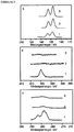
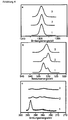
- Aluminum oxide, gallium oxide, neodymium oxide, magnesium oxide, hafnium oxide or zirconium oxide layers which are produced from the corresponding precursors, show a breakdown voltage between two conductors> 0.1 MV / cm. Preferably, breakdown voltages between 1 and 10 MV / cm. The breakdown voltage can be determined by means of the measuring and evaluation methods described in DIN EN ISO 2376: 2009-07.
- the indium-tin oxide layer has a resistivity (determined by four-point measurement) of ⁇ 10 -3 Ohm-cm.
- resistivities are between 10 -3 and 10 -5 ohm.cm.
- the conductivity can be determined by means of four-probe DC methods. This measuring method is described in DIN 50431 or ASTM F43-99.
- the indium-gallium-zinc oxide layers (IGZO) or the zinc-tin oxide layers (ZTO) have a charge carrier mobility> 10 -3 cm 2 / Vs.
- Charge carrier mobilities of 0.1 to 10 cm 2 / Vs are preferred.
- Another object of the present invention is the use of an organometallic aluminum, gallium, neodymium-ruthenium, magnesium, hafnium, zirconium, indium and / or tin complex or precursor for producing one or more functional layers in the field effect transistor.
- the substrate can be both a solid substrate such as glass, ceramic, metal or a plastic substrate and also a flexible substrate, in particular plastic film or metal foil.
- a flexible substrate film is used according to the invention.
- Preferred according to the invention is the TFT, with which large-area electronic circuits can be produced.
- the aluminum, gallium, neodymium, magnesium, hafnium or zirconium oxide layer has a thickness of 15 nm to 1 .mu.m, preferably 30 nm to 750 nm.
- the layer thickness depends on the particular coating technology used and its parameters , In the case of spin coating, these are, for example, the rotation speed and duration.
- the indium-tin-oxide layer has a thickness of 15 nm to 1 .mu.m, preferably 100 nm to 500 nm.
- the layer thickness depends on the particular coating technique used and its parameters. in the In the case of spin coating, these are, for example, the rotation speed and duration.
- the indium-gallium-zinc oxide (IGZO) or zinc-tin oxide (ZTO) layer has a thickness of 15 nm to 1 .mu.m, preferably 20 nm to 200 nm.
- the layer thickness depends on the particular coating technique used and its parameters. In the case of spin coating, these are, for example, the rotation speed and duration.
- the aforementioned electronic components consist of a field-effect transistor or thin-film transistor, which is composed of a gate, an insulating layer, a semiconductor and electrodes (drain and source).
- the gate preferably consists of a highly n-doped silicon wafer, a highly n-doped silicon thin film, conductive polymers (eg polypyrrolepolyaminobenzenesulfonic acid or polyethylenedioxythiophene-polystyrenesulfonic acid (PEDOT-PSS)), conductive ceramics (eg indium-tin-oxide (ITO) or Al, Ga or In-doped tin oxide (AZO, GZO, IZO) as well as F or Sb doped tin oxide (FTO, ATO)) or metals (eg gold, silver, titanium, zinc), depending on the design as a thin layer or substrate material.
- conductive polymers eg polypyrrolepolyaminobenzenesulfonic acid
- the thin layers may be applied in the arrangement below (bottom gate) or above (top gate) the semiconducting or insulating layer.
- the electronic component preferably has an insulating layer which consists of polymers (for example poly (4-vinylphenol), polymethyl methacrylate, polystyrene, polyimides or polycarbonate) or ceramics (for example silicon dioxide, silicon nitride, aluminum oxide, gallium oxide, neodymium oxide, magnesium oxide, hafnium oxide, zirconium oxide).
- the electronic device has a semiconductive layer composed of a semiconducting organic compound (e.g., polythiophene, oligothiophene, or polytriarylamine) or ceramics (e.g., zinc oxide, indium-gallium-zinc oxide (IGZO), or zinc-tin oxide (ZTO)).
- a semiconducting organic compound e.g., polythiophene, oligothiophene, or polytriarylamine
- ceramics e.g., zinc oxide, indium-gallium-zinc oxide (IGZO), or zinc-tin oxide (ZTO)
- the electronic component preferably has source and drain electrodes made of a highly n-doped silicon thin film, conductive polymers (eg polypyrrole-polyaminobenzenesulfonic acid or polyethylenedioxythiophene-polystyrenesulfonic acid (PEDOT-PSS)), conductive ceramics (eg indium tin oxide (ITO) or Al, Ga or In-doped tin oxide (AZO, GZO, IZO) and F or Sb-doped tin oxide (FTO, ATO)) or metals (eg gold, silver, titanium, zinc).
- the electrodes preferably designed as thin layers according to the invention
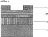
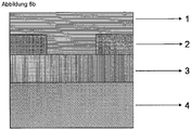
- the electrodes can be applied depending on the design in the arrangement below (bottom contact) or above (top contact) of the semiconducting or the insulating layer (see Figure 8a and b ).
- gate, insulator and semiconductor may be deposited unstructured by spin coating or dipcoating, as well as gaseous or liquid phase deposition techniques.
- Next can be gate, insulator, semiconductors and Electrodes structured by flexo / gravure printing, inkjet printing and deposition techniques from the gaseous or liquid phase can be applied. According to the invention, printing methods are preferred.
- This method produces both electronic components and the connections of individual components in integrated circuits.
- Example 2 Alkali metal-free preparation of the magnesium oxide precursor bis [2- (methoxyimino) propanoato] magnesium
- Example 3 Production of undoped magnesium oxide layers from the magnesium precursor with insulator properties (from Example 1 or 2)
- the magnesium oximat prepared according to Example 1 or 2 is applied to a substrate made of glass, ceramic or polymer by means of spin coating (or dipcoating or else inkjet printing). It is then annealed in air at temperatures above 210 ° C for 10 minutes.
- the magnesium oxide films thus obtained exhibit a uniform, crack-free, non-porous surface morphology.
- the layers consist of amorphous or nanocrystalline material. The layers have insulator properties.
- Example 4 Preparation of a zirconium dioxide precursor zirconium hydroxo [2- (methoxyimino) propanoate], Comparative Example
- the residue is taken up in 100 ml of dichloromethane and the resulting suspension is filtered again.
- the product is then precipitated from the filtrate with plenty of n-hexane, filtered off and dried in a desiccator. Yield 3.50 g.
- the compound thus obtained can be characterized by IR and NMR spectroscopy.
- Example 5 Preparation of zirconium oxide layers from the zirconium dioxide precursor
- the zirconium oxime prepared according to Example 4 is applied to a substrate made of glass, ceramic or polymer by means of spincoating (or dipcoating or else inkjet printing). Subsequently, in the air at temperatures above 200 ° C for 10 minutes annealed or UV irradiation with 150 mW / cm 2 carried out for 15 minutes.
- the zirconia films thus obtained exhibit a uniform, crack-free, non-porous surface morphology.
- the layers consist of amorphous or nanocrystalline material. The layers have insulator properties.
- the hafnium oxime prepared according to Example 6 is applied by spin coating (or dip coating or inkjet printing) to a substrate made of glass, ceramic or polymer. Subsequently, in the air at temperatures above 200 ° C for 10 minutes annealed or UV irradiation with 150 mW / cm 2 carried out for 15 minutes.
- the hafnium oxide films thus obtained exhibit a uniform, crack-free, non-porous surface morphology.
- the layers consist of amorphous or nanocrystalline material. The layers have insulator properties.
- Example 9 Preparation of alumina layers with insulator properties
- the Aluminiumoximat prepared according to Example 8 is applied by spin coating (or dip coating or inkjet printing) to a substrate made of glass, ceramic or polymer. Then it is added in the air Temperatures above 200 ° C annealed for 10 minutes or UV irradiation with 150 mW / cm 2 carried out for 15 minutes.
- the resulting alumina films exhibit a uniform, crack-free, non-porous surface morphology.
- the layers consist of nanocrystalline material.
- the layers have insulator properties.
- Example 11 Preparation of gallium oxide layers with insulator properties
- the gallium oximate produced according to Example 10 is applied to a substrate made of glass, ceramic or polymer by means of spin coating (or dipcoating or else inkjet printing). Subsequently, in the air at temperatures above 200 ° C for 10 minutes annealed or UV irradiation with 150 mW / cm 2 carried out for 15 minutes.
- the gallium oxide films thus obtained show a uniform, crack-free, non-porous Surface morphology.
- the layers consist of nanocrystalline material. The layers have insulator properties.
- Example 12 Preparation of a neodymium oxide precursor Tris [2- (methoxyimino) propanoato] neodymium, comparative example
- Example 13 Preparation of neodymium oxide layers with insulator properties
- the neodymium oxime produced according to Example 12 is applied to a substrate made of glass, ceramic or polymer by means of spin coating (or dipcoating or else inkjet printing). Subsequently, in the air at temperatures above 200 ° C for 10 minutes annealed or UV irradiation with 150 mW / cm 2 carried out for 15 minutes.
- the neodymium oxide films thus obtained exhibit a uniform, crack-free, non-porous surface morphology.
- the layers consist of nanocrystalline material. The layers have insulator properties.
- the Rutheniumoximat prepared according to Example 14 is applied by spin coating (or dip coating or inkjet printing) to a substrate made of glass, ceramic or polymer. Subsequently, in the air at temperatures above 200 ° C for 10 minutes annealed or UV irradiation with 150 mW / cm 2 carried out for 15 minutes.
- the resulting ruthenium oxide films exhibit a uniform, crack-free, non-porous surface morphology. Depending on the calcination temperature, the layers consist of nanocrystalline material.
- the example shows the production of a dielectric layer.
- a layer of zirconia is deposited by spin coating or printing and presented by subsequent calcination at 200 ° C for 10 minutes or UV irradiation at 150 mW / cm 2 for 15 minutes.
- the breakdown voltage for the dielectric layer can be determined to be 1 MV / cm.
- the example shows a field effect transistor (FET) according to Figures 8a and 8b.
- the device consists of a highly n-doped silicon wafer, on which the dielectric layer is applied.
- a semiconducting layer is shown, followed by an electrode structure made of metal, which is produced by vapor deposition of the metal or printing of a metal ink ( Figure 8a ).
- Figure 8b first the production of the electrode structure and then the application of the semiconductor layer can take place.
- the product is then precipitated from the filtrate with plenty of n-hexane, filtered off and dried in a desiccator. Yield 1.80 g (58.9%).
- the compound thus obtained can be characterized by IR and NMR spectroscopy.
- the residue is taken up in 100 ml of acetone or dimethoxyethane and the resulting suspension is filtered again.
- the product from the filtrate is precipitated with plenty of diethyl ether, filtered off and dried in a desiccator. Yield 3.7 g.
- the compound thus obtained can be characterized by IR and NMR spectroscopy.
- Example 20 Preparation of electrically conductive layers of indium tin oxide (ITO)
- the indium and Zinnoximate prepared according to Example 18 and 19 are brought together in a molar ratio of 90:10 in solution and applied by spin coating (or dip coating or inkjet printing) to a substrate made of glass, ceramic or polymer.
- the mixture is then tempered in air at temperatures above 200 ° C for 60 minutes or UV irradiation with 150 mW / cm 2 for 1 hour.
- the indium-tin oxide films thus obtained show a uniform, crack-free, non-porous Surface morphology.
- the layers consist of amorphous or nanocrystalline material.
- the layers have electrical conductivity.
- Example 21 Preparation of semiconductive layers of indium-gallium-zinc oxide (IGZO)
- indium and / or gallium oximes prepared according to Examples 10 and 18, as well as zinc oximes are dissolved in a suitable molar ratio.
- the solution thus obtained is applied by spin coating (or dipcoating or inkjet printing) to a substrate made of glass, ceramic or polymer.
- the mixture is then heated or air at temperatures above 200 ° C for 10 minutes of UV irradiation of 150 mW / cm 2 was carried out for 15 minutes.
- the indium-gallium-zinc oxide films thus obtained exhibit a uniform, crack-free, non-porous surface morphology.
- the layers are made of amorphous material. The layers have semiconducting properties.
- Example 22 Preparation of Semi-conductive Coatings from Zinc-Tin Oxide (ZTO)
- the tin oximes and zinc oximes prepared according to Example 19 are dissolved together in an appropriate ratio.
- tin contents Sn / (Sn + Zn) of 0 to 30 mole percent are suitable.
- the solution is applied to a glass, ceramic or polymer substrate by spin coating (or dipcoating, or else inkjet printing). Subsequently, in air at temperatures above 200 ° C annealed for 10 minutes or UV irradiation at 150 mW / cm 2 for 15 minutes.
- the resulting zinc-tin oxide films show a uniform, crack-free, non-porous surface morphology.
- the layers consist of amorphous or nanocrystalline material. The layers have semiconducting properties.
- Suitable solvents are 2-methoxyethanol, 2-butanol, methanol, dimethylformamide or mixtures thereof.
- the viscosity of the printing inks can be determined using a rheometer, eg MARS Rheometer from Haake. The determination is carried out under standard conditions (DIN 50 014-23).
Landscapes
- Chemical & Material Sciences (AREA)
- Organic Chemistry (AREA)
- Engineering & Computer Science (AREA)
- Materials Engineering (AREA)
- Chemical Kinetics & Catalysis (AREA)
- General Chemical & Material Sciences (AREA)
- Mechanical Engineering (AREA)
- Metallurgy (AREA)
- Thermal Sciences (AREA)
- Physics & Mathematics (AREA)
- Inorganic Chemistry (AREA)
- Life Sciences & Earth Sciences (AREA)
- Wood Science & Technology (AREA)
- Health & Medical Sciences (AREA)
- Toxicology (AREA)
- Ceramic Engineering (AREA)
- Thin Film Transistor (AREA)
- Parts Printed On Printed Circuit Boards (AREA)
- Organic Low-Molecular-Weight Compounds And Preparation Thereof (AREA)
- Non-Metallic Protective Coatings For Printed Circuits (AREA)
Claims (18)
- Précurseur pour le revêtement de composants électroniques, caractérisé en ce qu'il comprend un complexe organométallique de gallium, de ruthénium, de magnésium, d'hafnium, d'indium et/ou d'étain et des mélanges afférents, lequel complexe contient au moins un ligand pris parmi la classe des oximates.
- Précurseur selon la revendication 1, caractérisé en ce que le ligand est un 2-(méthoxyimino)alkanoate, un 2-(éthoxyimino)alkanoate ou un 2-(hydroxyimino)alkanoate.
- Composant électronique imprimé, lequel comporte les couches minces qui suivent :• un substrat conducteur solide ou flexible ou un substrat isolant comportant une couche conductrice (grille),• un isolant comprenant un oxyde d'aluminium, de gallium, de néodyme, de magnésium, d'hafnium ou de zirconium qui peut être obtenu à partir d'un précurseur correspondant, lequel précurseur contient un complexe organométallique d'aluminium, de gallium, de néodyme, de magnésium, d'hafnium ou de zirconium et des mélanges afférents, lequel complexe contient au moins un ligand pris parmi la classe des oximates,• au moins une électrode (électrode de drain),• un semiconducteur.
- Composant électronique imprimé, lequel comporte les couches minces qui suivent :• un substrat conducteur solide ou flexible ou un substrat isolant comportant une couche conductrice (grille) comprenant un oxyde d'indium et d'étain (ITO) qui peut être obtenu à partir du précurseur correspondant selon une ou plusieurs des revendications 1 à 3,• un isolant,• au moins une électrode (électrode de drain),• un semiconducteur.
- Composant électronique imprimé, lequel comporte les couches minces qui suivent :• un substrat conducteur solide ou flexible ou un substrat isolant comportant une couche conductrice (grille),• un isolant,• au moins une électrode (électrode de drain)• un semiconducteur comprenant un oxyde d'indium, de gallium et de zinc (IGZO) ou un oxyde de zinc et d'étain (ZTO) qui peut être obtenu à partir des précurseurs correspondants selon une ou plusieurs des revendications 1 à 3.
- Composant électronique imprimé selon la/les revendication(s) 3, 4 et/ou 5, caractérisé en ce que le substrat peut être à la fois un substrat solide, tel qu'un substrat en verre, en céramique, en métal ou en matière plastique, et un substrat flexible, en particulier un film en matière plastique ou une feuille en métal.
- Procédé pour la préparation d'un précurseur selon une ou plusieurs des revendications 1 ou 2, caractérisé en ce qu'au moins un acide oxocarboxylique est amené à réagir avec au moins un hydroxylamine ou un alkylhydroxylamine en présence d'une base, et un sel inorganique de gallium, de ruthénium, de magnésium, d'hafnium, d'indium et/ou d'étain et des mélanges afférents est ensuite ajouté.
- Procédé selon la revendication 7, caractérisé en ce que l'acide oxocarboxylique utilisé est de l'acide oxoacétique, de l'acide oxopropionique ou de l'acide oxobutyrique.
- Procédé pour la production de structures électroniques comportant une couche ou surface en oxyde d'aluminium, en oxyde de gallium, en oxyde de néodyme, en oxyde de ruthénium, en oxyde de magnésium, en oxyde d'hafnium, en oxyde de zirconium, en oxyde d'indium et/ou en oxyde d'étain et des mélanges afférents, caractérisé en ce que :a. des solutions de précurseur comprenant un complexe organométallique d'aluminium, de magnésium, de gallium, de néodyme, de ruthénium, d'hafnium, de zirconium, d'indium et/ou d'étain et des mélanges afférents, lesquelles contiennent au moins un ligand pris parmi la classe des oximates, sont appliquées sur un substrat selon soit une couche, soit plusieurs couches en correspondance avec la structure électronique destinée à être obtenue par revêtement/ dépôt par trempage/immersion, dépôt à la tournette/par centrifugation ou impression par jet d'encre ou impression flexographique/par gravure,b. la couche de précurseur appliquée est chauffée ou séchée dans l'air ou dans une atmosphère d'oxygène avec la formation d'une couche ou surface en oxyde d'aluminium, en oxyde de gallium, en oxyde de néodyme, en oxyde de ruthénium, en oxyde de magnésium, en oxyde d'hafnium, en oxyde de zirconium, en oxyde, d'indium et/ou en oxyde d'étain et des mélanges afférents,c. pour finir, la structure électronique résultant de l'application peut être scellée/rendue étanche au moyen d'une couche isolante et elle est munie de contacts et parachevée.
- Procédé selon la revendication 9, caractérisé en ce que la température pendant le chauffage T est ≥ 80°C.
- Procédé selon la revendication 9, caractérisé en ce que le chauffage ou le séchage est mis en oeuvre par irradiation avec une lumière UV présentant des longueurs d'onde < 400 nm.
- Procédé selon une ou plusieurs des revendications 9 à 11, caractérisé en ce que les couches en oxyde d'aluminium, en oxyde de gallium, en oxyde de néodyme, en oxyde de ruthénium, en oxyde de magnésium, en oxyde d'hafnium ou en oxyde de zirconium présentent une tension de rupture/claquage > 0,1 MV/cm entre deux conducteurs.
- Procédé selon une ou plusieurs des revendications 9 à 11, caractérisé en ce que la couche en oxyde d'indium et d'étain (couche en ITO) présente une résistance spécifique, déterminée au moyen d'une mesure en quatre points, < 10-3 ohm·cm.
- Procédé selon une ou plusieurs des revendications 9 à 11, caractérisé en ce que les couches en oxyde d'indium, de gallium et de zinc (IGZO) ou les couches en oxyde de zinc et d'étain (ZTO) présentent une mobilité de porteurs de charges > 10-3 cm2/Vs.
- Utilisation d'un précurseur, lequel comprend un complexe organométallique d'aluminium, de gallium, de néodyme, de ruthénium, de magnésium, d'hafnium, de zirconium, d'indium et/ou d'étain et des mélanges afférents, lequel complexe contient au moins un ligand pris parmi la classe des oximates pour le revêtement de composants électroniques.
- Utilisation selon la revendication 15, caractérisée en ce que le ligand est un 2-(méthoxyimino)alkanoate, un 2-(éthoxyimino)alkanoate ou un 2-(hydroxyimino)alkanoate.
- Utilisation selon la revendication 15 ou 16, caractérisée en ce que le précurseur est imprimable et est utilisé sous la forme d'une encre d'impression ou d'une pâte d'impression dans un transistor à effet de champ (FET) imprimé.
- Utilisation selon une ou plusieurs des revendications 15 à 17 pour la production d'une ou de plusieurs couche(s) fonctionnelle(s) dans un transistor à effet de champ.
Applications Claiming Priority (2)
| Application Number | Priority Date | Filing Date | Title |
|---|---|---|---|
| DE102009004491A DE102009004491A1 (de) | 2009-01-09 | 2009-01-09 | Funktionelles Material für gedruckte elektronische Bauteile |
| PCT/EP2009/008821 WO2010078907A1 (fr) | 2009-01-09 | 2009-12-10 | Matériau fonctionnel destiné à des composants électroniques imprimés |
Publications (2)
| Publication Number | Publication Date |
|---|---|
| EP2376434A1 EP2376434A1 (fr) | 2011-10-19 |
| EP2376434B1 true EP2376434B1 (fr) | 2017-05-24 |
Family
ID=42016966
Family Applications (1)
| Application Number | Title | Priority Date | Filing Date |
|---|---|---|---|
| EP09799248.1A Not-in-force EP2376434B1 (fr) | 2009-01-09 | 2009-12-10 | Matériau fonctionnel destiné à des composants électroniques imprimés |
Country Status (8)
| Country | Link |
|---|---|
| US (1) | US8766251B2 (fr) |
| EP (1) | EP2376434B1 (fr) |
| JP (1) | JP5798041B2 (fr) |
| KR (1) | KR101724758B1 (fr) |
| CN (2) | CN102272094B (fr) |
| DE (1) | DE102009004491A1 (fr) |
| TW (1) | TWI495630B (fr) |
| WO (1) | WO2010078907A1 (fr) |
Families Citing this family (24)
| Publication number | Priority date | Publication date | Assignee | Title |
|---|---|---|---|---|
| KR20130034662A (ko) * | 2010-06-29 | 2013-04-05 | 메르크 파텐트 게엠베하 | 반도체막의 제조 |
| US20120082865A1 (en) * | 2010-10-01 | 2012-04-05 | Agency For Science, Technology And Research | Method for forming a magnetic recording medium and a magnetic recording medium formed thereof |
| WO2012163464A1 (fr) | 2011-06-01 | 2012-12-06 | Merck Patent Gmbh | Tft ambipolaires hybrides |
| DE102012006045A1 (de) | 2012-03-27 | 2013-10-02 | Merck Patent Gmbh | Verfahren zur Herstellung elektrisch halbleitender oder leitender Schichten mit verbesserter Leitfähigkeit |
| CN104081498A (zh) * | 2012-01-27 | 2014-10-01 | 默克专利有限公司 | 生产具有改进电导率的半导电或导电层的方法 |
| DE102012001508A1 (de) | 2012-01-27 | 2013-08-01 | Merck Patent Gmbh | Verfahren zur Herstellung elektrisch halbleitender oder leitender Schichten mit verbesserter Leitfähigkeit |
| TWI512840B (zh) * | 2012-02-14 | 2015-12-11 | Innocom Tech Shenzhen Co Ltd | 薄膜電晶體及其製作方法及顯示器 |
| CN104284952A (zh) * | 2012-02-29 | 2015-01-14 | 耶路撒冷希伯来大学伊森姆研究发展有限公司 | 包含金属前体纳米颗粒的油墨 |
| CH706216A1 (de) * | 2012-03-12 | 2013-09-13 | Von Roll Solar Ag | Substrat für elektrische oder elektronische Bauteile. |
| WO2014021850A1 (fr) | 2012-07-31 | 2014-02-06 | Hewlett-Packard Development Company, L.P. | Pile de couches minces |
| EP2852989B1 (fr) | 2012-07-31 | 2016-11-30 | Hewlett-Packard Development Company, L.P. | Pile de couches minces |
| DE102012218647A1 (de) * | 2012-10-12 | 2014-04-17 | Schneider Electric Industries Sas | Bedieneinheit |
| US20150303397A1 (en) * | 2012-12-17 | 2015-10-22 | Merck Patent Gmbh | Inorganic barrier layers |
| KR101288106B1 (ko) * | 2012-12-20 | 2013-07-26 | (주)피이솔브 | 금속 전구체 및 이를 이용한 금속 전구체 잉크 |
| CN103236402B (zh) * | 2013-04-27 | 2016-02-03 | 京东方科技集团股份有限公司 | 薄膜晶体管及其制作方法、阵列基板及显示装置 |
| EP3011373B1 (fr) | 2013-06-20 | 2017-11-15 | Merck Patent GmbH | Procede de commande des proprietes optiques de couches filtrant les uv |
| CN105934535A (zh) * | 2014-01-31 | 2016-09-07 | 默克专利股份有限公司 | 制备uv光检测器的方法 |
| US9982154B2 (en) * | 2014-04-17 | 2018-05-29 | Electroninks Incorporated | Solid ink composition |
| US9768254B2 (en) | 2015-07-30 | 2017-09-19 | International Business Machines Corporation | Leakage-free implantation-free ETSOI transistors |
| KR102208520B1 (ko) | 2016-07-19 | 2021-01-26 | 어플라이드 머티어리얼스, 인코포레이티드 | 디스플레이 디바이스들에서 활용되는 지르코늄 산화물을 포함하는 하이-k 유전체 재료들 |
| CN108022828B (zh) * | 2017-11-13 | 2021-05-14 | 华南理工大学 | 一种uv预处理衬底改善打印氧化物薄膜形貌的方法 |
| JP2020011859A (ja) * | 2018-07-17 | 2020-01-23 | トヨタ自動車株式会社 | 成膜方法、及び、半導体装置の製造方法 |
| DE102018217977A1 (de) * | 2018-10-22 | 2020-04-23 | Zf Friedrichshafen Ag | Verfahren und Vorrichtung zum Anpassen von PWM-Werten einer feldorientierten Regelung einer elektrischen Maschine |
| EP4343432A1 (fr) * | 2022-09-22 | 2024-03-27 | Paul Scherrer Institut | Utilisation d'un cétoacidoximate comprenant un métal et/ou un métalloide et/ou d'un composé métallique comprenant du cétoacidoximate en tant qu'agent de formation de motifs |
Family Cites Families (16)
| Publication number | Priority date | Publication date | Assignee | Title |
|---|---|---|---|---|
| JP2556317B2 (ja) * | 1986-12-25 | 1996-11-20 | 日本曹達株式会社 | イミノアセチル誘導体,その製造方法及び殺菌剤 |
| CA2110097C (fr) * | 1992-11-30 | 2002-07-09 | Soichiro Kawakami | Batterie secondaire |
| DE19851703A1 (de) | 1998-10-30 | 2000-05-04 | Inst Halbleiterphysik Gmbh | Verfahren zur Herstellung von elektronischen Strukturen |
| JP2000133197A (ja) | 1998-10-30 | 2000-05-12 | Applied Materials Inc | イオン注入装置 |
| WO2002015264A2 (fr) | 2000-08-18 | 2002-02-21 | Siemens Aktiengesellschaft | Composant electronique organique encapsule, son procede de production et son utilisation |
| WO2004063806A1 (fr) | 2003-01-09 | 2004-07-29 | Polyic Gmbh & Co. Kg | Platine ou substrat pour un appareil electronique organique et utilisation de ladite platine |
| US7253735B2 (en) | 2003-03-24 | 2007-08-07 | Alien Technology Corporation | RFID tags and processes for producing RFID tags |
| US6875661B2 (en) | 2003-07-10 | 2005-04-05 | International Business Machines Corporation | Solution deposition of chalcogenide films |
| US6867081B2 (en) | 2003-07-31 | 2005-03-15 | Hewlett-Packard Development Company, L.P. | Solution-processed thin film transistor formation method |
| US7145174B2 (en) * | 2004-03-12 | 2006-12-05 | Hewlett-Packard Development Company, Lp. | Semiconductor device |
| US7242039B2 (en) * | 2004-03-12 | 2007-07-10 | Hewlett-Packard Development Company, L.P. | Semiconductor device |
| GB2416428A (en) | 2004-07-19 | 2006-01-25 | Seiko Epson Corp | Method for fabricating a semiconductor element from a dispersion of semiconductor particles |
| JP5177954B2 (ja) * | 2006-01-30 | 2013-04-10 | キヤノン株式会社 | 電界効果型トランジスタ |
| JP5196870B2 (ja) * | 2007-05-23 | 2013-05-15 | キヤノン株式会社 | 酸化物半導体を用いた電子素子及びその製造方法 |
| DE102007043920A1 (de) * | 2007-07-17 | 2009-01-22 | Merck Patent Gmbh | Funktionelles Material für gedruckte elektronische Bauteile |
| JP5396709B2 (ja) * | 2007-12-11 | 2014-01-22 | セイコーエプソン株式会社 | 薄膜トランジスタ、電気光学装置および電子機器 |
-
2009
- 2009-01-09 DE DE102009004491A patent/DE102009004491A1/de not_active Withdrawn
- 2009-12-10 EP EP09799248.1A patent/EP2376434B1/fr not_active Not-in-force
- 2009-12-10 KR KR1020117018509A patent/KR101724758B1/ko not_active Expired - Fee Related
- 2009-12-10 CN CN200980154098.3A patent/CN102272094B/zh not_active Expired - Fee Related
- 2009-12-10 CN CN201410641734.8A patent/CN104530815B/zh not_active Expired - Fee Related
- 2009-12-10 WO PCT/EP2009/008821 patent/WO2010078907A1/fr not_active Ceased
- 2009-12-10 JP JP2011544796A patent/JP5798041B2/ja not_active Expired - Fee Related
- 2009-12-10 US US13/143,837 patent/US8766251B2/en not_active Expired - Fee Related
- 2009-12-30 TW TW098146018A patent/TWI495630B/zh not_active IP Right Cessation
Non-Patent Citations (1)
| Title |
|---|
| None * |
Also Published As
| Publication number | Publication date |
|---|---|
| CN102272094A (zh) | 2011-12-07 |
| DE102009004491A1 (de) | 2010-07-15 |
| CN102272094B (zh) | 2015-04-22 |
| CN104530815B (zh) | 2017-06-06 |
| CN104530815A (zh) | 2015-04-22 |
| TWI495630B (zh) | 2015-08-11 |
| JP5798041B2 (ja) | 2015-10-21 |
| WO2010078907A1 (fr) | 2010-07-15 |
| KR101724758B1 (ko) | 2017-04-07 |
| US20110272691A1 (en) | 2011-11-10 |
| TW201035018A (en) | 2010-10-01 |
| EP2376434A1 (fr) | 2011-10-19 |
| KR20110102509A (ko) | 2011-09-16 |
| JP2012514611A (ja) | 2012-06-28 |
| US8766251B2 (en) | 2014-07-01 |
Similar Documents
| Publication | Publication Date | Title |
|---|---|---|
| EP2376434B1 (fr) | Matériau fonctionnel destiné à des composants électroniques imprimés | |
| DE102007043920A1 (de) | Funktionelles Material für gedruckte elektronische Bauteile | |
| US8013331B2 (en) | Thin film transistor, method of manufacturing the same, and electronic device using the same | |
| CN103959478B (zh) | 制造金属氧化物层的方法,用该方法制造的层及其用途 | |
| US9194046B2 (en) | Method for producing semiconducting indium oxide layers, indium oxide layers produced according to said method and their use | |
| WO2010094581A1 (fr) | Compositions contenant un alcoolate d'indium, leur procédé de fabrication et leur utilisation | |
| US20140367676A1 (en) | Process for the production of electrically semiconducting or conducting metal-oxide layers having improved conductivity | |
| KR102032168B1 (ko) | 산화 인듐-함유 층 제조 방법 | |
| EP2839504A1 (fr) | Formulation contenant des composés ammoniacaux d'hydroxo-zinc | |
| Liu et al. | Compact and ultrathin multi-element oxide films grown by temperature-controlled deposition and their surface-potential based transistor theoretical simulation model | |
| DE102012001508A1 (de) | Verfahren zur Herstellung elektrisch halbleitender oder leitender Schichten mit verbesserter Leitfähigkeit | |
| DE102012006045A1 (de) | Verfahren zur Herstellung elektrisch halbleitender oder leitender Schichten mit verbesserter Leitfähigkeit | |
| KR102682396B1 (ko) | 금속 산화물 박막용 용액 조성물 및 이를 사용한 금속 산화물 박막의 제조 방법 | |
| DE102012201840A1 (de) | Halbleiterzusammensetzung |
Legal Events
| Date | Code | Title | Description |
|---|---|---|---|
| PUAI | Public reference made under article 153(3) epc to a published international application that has entered the european phase |
Free format text: ORIGINAL CODE: 0009012 |
|
| 17P | Request for examination filed |
Effective date: 20110519 |
|
| AK | Designated contracting states |
Kind code of ref document: A1 Designated state(s): AT BE BG CH CY CZ DE DK EE ES FI FR GB GR HR HU IE IS IT LI LT LU LV MC MK MT NL NO PL PT RO SE SI SK SM TR |
|
| RIN1 | Information on inventor provided before grant (corrected) |
Inventor name: HOFFMANN, RUDOLF Inventor name: SCHNEIDER, JOERG J. Inventor name: RENKER, SABINE Inventor name: KLYSZCZ, ANDREAS Inventor name: KUEGLER, RALF |
|
| DAX | Request for extension of the european patent (deleted) | ||
| 17Q | First examination report despatched |
Effective date: 20130228 |
|
| GRAP | Despatch of communication of intention to grant a patent |
Free format text: ORIGINAL CODE: EPIDOSNIGR1 |
|
| INTG | Intention to grant announced |
Effective date: 20161109 |
|
| GRAS | Grant fee paid |
Free format text: ORIGINAL CODE: EPIDOSNIGR3 |
|
| GRAJ | Information related to disapproval of communication of intention to grant by the applicant or resumption of examination proceedings by the epo deleted |
Free format text: ORIGINAL CODE: EPIDOSDIGR1 |
|
| GRAL | Information related to payment of fee for publishing/printing deleted |
Free format text: ORIGINAL CODE: EPIDOSDIGR3 |
|
| INTC | Intention to grant announced (deleted) | ||
| GRAR | Information related to intention to grant a patent recorded |
Free format text: ORIGINAL CODE: EPIDOSNIGR71 |
|
| GRAA | (expected) grant |
Free format text: ORIGINAL CODE: 0009210 |
|
| INTG | Intention to grant announced |
Effective date: 20170412 |
|
| AK | Designated contracting states |
Kind code of ref document: B1 Designated state(s): AT BE BG CH CY CZ DE DK EE ES FI FR GB GR HR HU IE IS IT LI LT LU LV MC MK MT NL NO PL PT RO SE SI SK SM TR |
|
| REG | Reference to a national code |
Ref country code: GB Ref legal event code: FG4D Free format text: NOT ENGLISH |
|
| REG | Reference to a national code |
Ref country code: CH Ref legal event code: EP |
|
| REG | Reference to a national code |
Ref country code: IE Ref legal event code: FG4D Free format text: LANGUAGE OF EP DOCUMENT: GERMAN |
|
| REG | Reference to a national code |
Ref country code: AT Ref legal event code: REF Ref document number: 895959 Country of ref document: AT Kind code of ref document: T Effective date: 20170615 |
|
| REG | Reference to a national code |
Ref country code: DE Ref legal event code: R096 Ref document number: 502009014008 Country of ref document: DE |
|
| REG | Reference to a national code |
Ref country code: NL Ref legal event code: FP |
|
| REG | Reference to a national code |
Ref country code: LT Ref legal event code: MG4D |
|
| PG25 | Lapsed in a contracting state [announced via postgrant information from national office to epo] |
Ref country code: NO Free format text: LAPSE BECAUSE OF FAILURE TO SUBMIT A TRANSLATION OF THE DESCRIPTION OR TO PAY THE FEE WITHIN THE PRESCRIBED TIME-LIMIT Effective date: 20170824 Ref country code: HR Free format text: LAPSE BECAUSE OF FAILURE TO SUBMIT A TRANSLATION OF THE DESCRIPTION OR TO PAY THE FEE WITHIN THE PRESCRIBED TIME-LIMIT Effective date: 20170524 Ref country code: FI Free format text: LAPSE BECAUSE OF FAILURE TO SUBMIT A TRANSLATION OF THE DESCRIPTION OR TO PAY THE FEE WITHIN THE PRESCRIBED TIME-LIMIT Effective date: 20170524 Ref country code: ES Free format text: LAPSE BECAUSE OF FAILURE TO SUBMIT A TRANSLATION OF THE DESCRIPTION OR TO PAY THE FEE WITHIN THE PRESCRIBED TIME-LIMIT Effective date: 20170524 Ref country code: LT Free format text: LAPSE BECAUSE OF FAILURE TO SUBMIT A TRANSLATION OF THE DESCRIPTION OR TO PAY THE FEE WITHIN THE PRESCRIBED TIME-LIMIT Effective date: 20170524 Ref country code: GR Free format text: LAPSE BECAUSE OF FAILURE TO SUBMIT A TRANSLATION OF THE DESCRIPTION OR TO PAY THE FEE WITHIN THE PRESCRIBED TIME-LIMIT Effective date: 20170825 |
|
| REG | Reference to a national code |
Ref country code: FR Ref legal event code: PLFP Year of fee payment: 9 |
|
| PG25 | Lapsed in a contracting state [announced via postgrant information from national office to epo] |
Ref country code: LV Free format text: LAPSE BECAUSE OF FAILURE TO SUBMIT A TRANSLATION OF THE DESCRIPTION OR TO PAY THE FEE WITHIN THE PRESCRIBED TIME-LIMIT Effective date: 20170524 Ref country code: BG Free format text: LAPSE BECAUSE OF FAILURE TO SUBMIT A TRANSLATION OF THE DESCRIPTION OR TO PAY THE FEE WITHIN THE PRESCRIBED TIME-LIMIT Effective date: 20170824 Ref country code: SE Free format text: LAPSE BECAUSE OF FAILURE TO SUBMIT A TRANSLATION OF THE DESCRIPTION OR TO PAY THE FEE WITHIN THE PRESCRIBED TIME-LIMIT Effective date: 20170524 Ref country code: IS Free format text: LAPSE BECAUSE OF FAILURE TO SUBMIT A TRANSLATION OF THE DESCRIPTION OR TO PAY THE FEE WITHIN THE PRESCRIBED TIME-LIMIT Effective date: 20170924 |
|
| PG25 | Lapsed in a contracting state [announced via postgrant information from national office to epo] |
Ref country code: CZ Free format text: LAPSE BECAUSE OF FAILURE TO SUBMIT A TRANSLATION OF THE DESCRIPTION OR TO PAY THE FEE WITHIN THE PRESCRIBED TIME-LIMIT Effective date: 20170524 Ref country code: DK Free format text: LAPSE BECAUSE OF FAILURE TO SUBMIT A TRANSLATION OF THE DESCRIPTION OR TO PAY THE FEE WITHIN THE PRESCRIBED TIME-LIMIT Effective date: 20170524 Ref country code: SK Free format text: LAPSE BECAUSE OF FAILURE TO SUBMIT A TRANSLATION OF THE DESCRIPTION OR TO PAY THE FEE WITHIN THE PRESCRIBED TIME-LIMIT Effective date: 20170524 Ref country code: RO Free format text: LAPSE BECAUSE OF FAILURE TO SUBMIT A TRANSLATION OF THE DESCRIPTION OR TO PAY THE FEE WITHIN THE PRESCRIBED TIME-LIMIT Effective date: 20170524 Ref country code: EE Free format text: LAPSE BECAUSE OF FAILURE TO SUBMIT A TRANSLATION OF THE DESCRIPTION OR TO PAY THE FEE WITHIN THE PRESCRIBED TIME-LIMIT Effective date: 20170524 |
|
| REG | Reference to a national code |
Ref country code: DE Ref legal event code: R097 Ref document number: 502009014008 Country of ref document: DE |
|
| PG25 | Lapsed in a contracting state [announced via postgrant information from national office to epo] |
Ref country code: SM Free format text: LAPSE BECAUSE OF FAILURE TO SUBMIT A TRANSLATION OF THE DESCRIPTION OR TO PAY THE FEE WITHIN THE PRESCRIBED TIME-LIMIT Effective date: 20170524 Ref country code: IT Free format text: LAPSE BECAUSE OF FAILURE TO SUBMIT A TRANSLATION OF THE DESCRIPTION OR TO PAY THE FEE WITHIN THE PRESCRIBED TIME-LIMIT Effective date: 20170524 Ref country code: PL Free format text: LAPSE BECAUSE OF FAILURE TO SUBMIT A TRANSLATION OF THE DESCRIPTION OR TO PAY THE FEE WITHIN THE PRESCRIBED TIME-LIMIT Effective date: 20170524 |
|
| PLBE | No opposition filed within time limit |
Free format text: ORIGINAL CODE: 0009261 |
|
| STAA | Information on the status of an ep patent application or granted ep patent |
Free format text: STATUS: NO OPPOSITION FILED WITHIN TIME LIMIT |
|
| 26N | No opposition filed |
Effective date: 20180227 |
|
| PG25 | Lapsed in a contracting state [announced via postgrant information from national office to epo] |
Ref country code: SI Free format text: LAPSE BECAUSE OF FAILURE TO SUBMIT A TRANSLATION OF THE DESCRIPTION OR TO PAY THE FEE WITHIN THE PRESCRIBED TIME-LIMIT Effective date: 20170524 |
|
| REG | Reference to a national code |
Ref country code: CH Ref legal event code: PL |
|
| REG | Reference to a national code |
Ref country code: IE Ref legal event code: MM4A |
|
| PG25 | Lapsed in a contracting state [announced via postgrant information from national office to epo] |
Ref country code: LU Free format text: LAPSE BECAUSE OF NON-PAYMENT OF DUE FEES Effective date: 20171210 Ref country code: MT Free format text: LAPSE BECAUSE OF FAILURE TO SUBMIT A TRANSLATION OF THE DESCRIPTION OR TO PAY THE FEE WITHIN THE PRESCRIBED TIME-LIMIT Effective date: 20170524 |
|
| REG | Reference to a national code |
Ref country code: BE Ref legal event code: MM Effective date: 20171231 |
|
| PG25 | Lapsed in a contracting state [announced via postgrant information from national office to epo] |
Ref country code: IE Free format text: LAPSE BECAUSE OF NON-PAYMENT OF DUE FEES Effective date: 20171210 |
|
| PG25 | Lapsed in a contracting state [announced via postgrant information from national office to epo] |
Ref country code: LI Free format text: LAPSE BECAUSE OF NON-PAYMENT OF DUE FEES Effective date: 20171231 Ref country code: CH Free format text: LAPSE BECAUSE OF NON-PAYMENT OF DUE FEES Effective date: 20171231 Ref country code: BE Free format text: LAPSE BECAUSE OF NON-PAYMENT OF DUE FEES Effective date: 20171231 |
|
| REG | Reference to a national code |
Ref country code: AT Ref legal event code: MM01 Ref document number: 895959 Country of ref document: AT Kind code of ref document: T Effective date: 20171210 |
|
| PG25 | Lapsed in a contracting state [announced via postgrant information from national office to epo] |
Ref country code: AT Free format text: LAPSE BECAUSE OF NON-PAYMENT OF DUE FEES Effective date: 20171210 |
|
| PG25 | Lapsed in a contracting state [announced via postgrant information from national office to epo] |
Ref country code: MC Free format text: LAPSE BECAUSE OF FAILURE TO SUBMIT A TRANSLATION OF THE DESCRIPTION OR TO PAY THE FEE WITHIN THE PRESCRIBED TIME-LIMIT Effective date: 20170524 Ref country code: HU Free format text: LAPSE BECAUSE OF FAILURE TO SUBMIT A TRANSLATION OF THE DESCRIPTION OR TO PAY THE FEE WITHIN THE PRESCRIBED TIME-LIMIT; INVALID AB INITIO Effective date: 20091210 |
|
| PG25 | Lapsed in a contracting state [announced via postgrant information from national office to epo] |
Ref country code: CY Free format text: LAPSE BECAUSE OF NON-PAYMENT OF DUE FEES Effective date: 20170524 |
|
| PG25 | Lapsed in a contracting state [announced via postgrant information from national office to epo] |
Ref country code: MK Free format text: LAPSE BECAUSE OF FAILURE TO SUBMIT A TRANSLATION OF THE DESCRIPTION OR TO PAY THE FEE WITHIN THE PRESCRIBED TIME-LIMIT Effective date: 20170524 |
|
| PGFP | Annual fee paid to national office [announced via postgrant information from national office to epo] |
Ref country code: DE Payment date: 20191126 Year of fee payment: 11 Ref country code: NL Payment date: 20191114 Year of fee payment: 11 |
|
| PGFP | Annual fee paid to national office [announced via postgrant information from national office to epo] |
Ref country code: FR Payment date: 20191115 Year of fee payment: 11 |
|
| PG25 | Lapsed in a contracting state [announced via postgrant information from national office to epo] |
Ref country code: TR Free format text: LAPSE BECAUSE OF FAILURE TO SUBMIT A TRANSLATION OF THE DESCRIPTION OR TO PAY THE FEE WITHIN THE PRESCRIBED TIME-LIMIT Effective date: 20170524 |
|
| PGFP | Annual fee paid to national office [announced via postgrant information from national office to epo] |
Ref country code: GB Payment date: 20191206 Year of fee payment: 11 |
|
| PG25 | Lapsed in a contracting state [announced via postgrant information from national office to epo] |
Ref country code: PT Free format text: LAPSE BECAUSE OF FAILURE TO SUBMIT A TRANSLATION OF THE DESCRIPTION OR TO PAY THE FEE WITHIN THE PRESCRIBED TIME-LIMIT Effective date: 20170524 |
|
| REG | Reference to a national code |
Ref country code: DE Ref legal event code: R119 Ref document number: 502009014008 Country of ref document: DE |
|
| REG | Reference to a national code |
Ref country code: NL Ref legal event code: MM Effective date: 20210101 |
|
| GBPC | Gb: european patent ceased through non-payment of renewal fee |
Effective date: 20201210 |
|
| PG25 | Lapsed in a contracting state [announced via postgrant information from national office to epo] |
Ref country code: NL Free format text: LAPSE BECAUSE OF NON-PAYMENT OF DUE FEES Effective date: 20210101 |
|
| PG25 | Lapsed in a contracting state [announced via postgrant information from national office to epo] |
Ref country code: FR Free format text: LAPSE BECAUSE OF NON-PAYMENT OF DUE FEES Effective date: 20201231 |
|
| PG25 | Lapsed in a contracting state [announced via postgrant information from national office to epo] |
Ref country code: DE Free format text: LAPSE BECAUSE OF NON-PAYMENT OF DUE FEES Effective date: 20210701 Ref country code: GB Free format text: LAPSE BECAUSE OF NON-PAYMENT OF DUE FEES Effective date: 20201210 |