EP2378352A2 - Flachbildschirm - Google Patents
Flachbildschirm Download PDFInfo
- Publication number
- EP2378352A2 EP2378352A2 EP11158336A EP11158336A EP2378352A2 EP 2378352 A2 EP2378352 A2 EP 2378352A2 EP 11158336 A EP11158336 A EP 11158336A EP 11158336 A EP11158336 A EP 11158336A EP 2378352 A2 EP2378352 A2 EP 2378352A2
- Authority
- EP
- European Patent Office
- Prior art keywords
- flat panel
- panel display
- light
- sensing unit
- photosensor
- Prior art date
- Legal status (The legal status is an assumption and is not a legal conclusion. Google has not performed a legal analysis and makes no representation as to the accuracy of the status listed.)
- Granted
Links
Images



Classifications
-
- G—PHYSICS
- G02—OPTICS
- G02F—OPTICAL DEVICES OR ARRANGEMENTS FOR THE CONTROL OF LIGHT BY MODIFICATION OF THE OPTICAL PROPERTIES OF THE MEDIA OF THE ELEMENTS INVOLVED THEREIN; NON-LINEAR OPTICS; FREQUENCY-CHANGING OF LIGHT; OPTICAL LOGIC ELEMENTS; OPTICAL ANALOGUE/DIGITAL CONVERTERS
- G02F1/00—Devices or arrangements for the control of the intensity, colour, phase, polarisation or direction of light arriving from an independent light source, e.g. switching, gating or modulating; Non-linear optics
- G02F1/01—Devices or arrangements for the control of the intensity, colour, phase, polarisation or direction of light arriving from an independent light source, e.g. switching, gating or modulating; Non-linear optics for the control of the intensity, phase, polarisation or colour
- G02F1/13—Devices or arrangements for the control of the intensity, colour, phase, polarisation or direction of light arriving from an independent light source, e.g. switching, gating or modulating; Non-linear optics for the control of the intensity, phase, polarisation or colour based on liquid crystals, e.g. single liquid crystal display cells
- G02F1/133—Constructional arrangements; Operation of liquid crystal cells; Circuit arrangements
- G02F1/13306—Circuit arrangements or driving methods for the control of single liquid crystal cells
- G02F1/13318—Circuits comprising a photodetector
-
- G—PHYSICS
- G02—OPTICS
- G02F—OPTICAL DEVICES OR ARRANGEMENTS FOR THE CONTROL OF LIGHT BY MODIFICATION OF THE OPTICAL PROPERTIES OF THE MEDIA OF THE ELEMENTS INVOLVED THEREIN; NON-LINEAR OPTICS; FREQUENCY-CHANGING OF LIGHT; OPTICAL LOGIC ELEMENTS; OPTICAL ANALOGUE/DIGITAL CONVERTERS
- G02F1/00—Devices or arrangements for the control of the intensity, colour, phase, polarisation or direction of light arriving from an independent light source, e.g. switching, gating or modulating; Non-linear optics
- G02F1/01—Devices or arrangements for the control of the intensity, colour, phase, polarisation or direction of light arriving from an independent light source, e.g. switching, gating or modulating; Non-linear optics for the control of the intensity, phase, polarisation or colour
- G02F1/13—Devices or arrangements for the control of the intensity, colour, phase, polarisation or direction of light arriving from an independent light source, e.g. switching, gating or modulating; Non-linear optics for the control of the intensity, phase, polarisation or colour based on liquid crystals, e.g. single liquid crystal display cells
- G02F1/133—Constructional arrangements; Operation of liquid crystal cells; Circuit arrangements
- G02F1/13306—Circuit arrangements or driving methods for the control of single liquid crystal cells
- G02F1/13312—Circuits comprising photodetectors for purposes other than feedback
-
- G—PHYSICS
- G09—EDUCATION; CRYPTOGRAPHY; DISPLAY; ADVERTISING; SEALS
- G09G—ARRANGEMENTS OR CIRCUITS FOR CONTROL OF INDICATING DEVICES USING STATIC MEANS TO PRESENT VARIABLE INFORMATION
- G09G3/00—Control arrangements or circuits, of interest only in connection with visual indicators other than cathode-ray tubes
- G09G3/20—Control arrangements or circuits, of interest only in connection with visual indicators other than cathode-ray tubes for presentation of an assembly of a number of characters, e.g. a page, by composing the assembly by combination of individual elements arranged in a matrix no fixed position being assigned to or needed to be assigned to the individual characters or partial characters
- G09G3/34—Control arrangements or circuits, of interest only in connection with visual indicators other than cathode-ray tubes for presentation of an assembly of a number of characters, e.g. a page, by composing the assembly by combination of individual elements arranged in a matrix no fixed position being assigned to or needed to be assigned to the individual characters or partial characters by control of light from an independent source
- G09G3/3406—Control of illumination source
-
- H—ELECTRICITY
- H10—SEMICONDUCTOR DEVICES; ELECTRIC SOLID-STATE DEVICES NOT OTHERWISE PROVIDED FOR
- H10K—ORGANIC ELECTRIC SOLID-STATE DEVICES
- H10K59/00—Integrated devices, or assemblies of multiple devices, comprising at least one organic light-emitting element covered by group H10K50/00
- H10K59/60—OLEDs integrated with inorganic light-sensitive elements, e.g. with inorganic solar cells or inorganic photodiodes
-
- G—PHYSICS
- G09—EDUCATION; CRYPTOGRAPHY; DISPLAY; ADVERTISING; SEALS
- G09G—ARRANGEMENTS OR CIRCUITS FOR CONTROL OF INDICATING DEVICES USING STATIC MEANS TO PRESENT VARIABLE INFORMATION
- G09G2360/00—Aspects of the architecture of display systems
- G09G2360/14—Detecting light within display terminals, e.g. using a single or a plurality of photosensors
- G09G2360/144—Detecting light within display terminals, e.g. using a single or a plurality of photosensors the light being ambient light
Definitions
- the present invention relates to a flat panel display.
- Photosensors that convert light signals to electrical signals are being developed to provide various functions owing to the developments of the optical industry and the semiconductor industry.
- photosensors are built in mobile devices including display units such as mobile phones, digital cameras, and personal digital assistances (PDAs).
- Display units such as mobile phones, digital cameras, and personal digital assistances (PDAs).
- Image display apparatuses such as liquid crystal displays (LCDs) and organic light emitting devices (OLEDs) may be used to provide touch panel functions to the display devices.
- LCDs liquid crystal displays
- OLEDs organic light emitting devices
- photosensors used in LCDs may be used to adjust the intensity of light emitted from a backlight by sensing external light. Therefore, research involving the use of photosensors to improve the quality of image display apparatuses is ongoing.
- an aspect of the present invention provides a flat panel display capable of calculating a tilt angle (e.g., a gradient) of the flat panel display by using a difference between intensities of light incident on two or more different photosensors.
- a tilt angle e.g., a gradient
- a flat panel display including: a first substrate including an emission region and a non-emission region; a light emission unit on the emission region; a first sensing unit on the non-emission region; and a second sensing unit on the non-emission region, wherein the first and second sensing units are arranged to allow determination of a tilt angle of the flat panel display using light intensities measured by the first and second sensing units.
- the flat panel display may further include a second substrate on the light emission unit and a bonding member for bonding the first substrate and the second substrate together.
- the flat panel display may comprise means for selectively blocking the light path of external light falling on one of the first and second sensing units as the display is tilted.
- the selective blocking means is, for example, one or more light shielding members that are arranged to progressively shield one of the sensing units from external light as the display is tilted.
- the first sensing unit may include a first photosensor and the second sensing unit may include a second photosensor and a light shielding member.
- the light shielding member may be adjacent the second photosensor.
- the light shielding member may be adjacent at least one side of the second photosensor.
- the light shielding member may contact a side of the second photosensor.
- a height of the light shielding member may be greater than a height of the second photosensor.
- a width of the light shielding member may be less than or equal to a width of the second photosensor.
- the light shielding member may be pillar-shaped.
- the light shielding member may be perpendicular to a surface of the first substrate.
- a height of the light shielding member may be less than or equal to a height of the bonding member.
- the first sensing unit may be configured to measure a first intensity of light incident on the first sensing unit
- the second sensing unit may be configured to measure a second intensity of light incident on the second sensing unit, such that the tilt angle of the flat panel display may be determinable by comparing the second light intensity to the first light intensity.
- the second light intensity may be reduced at a rate that exceeds a rate of reduction of the first light intensity as the flat panel display is tilted.
- the first sensing unit may be configured to measure a first intensity of light incident on the first sensing unit
- the second sensing unit may be configured to measure a second intensity of light incident on the second sensing unit, such that the tilt angle of the flat panel display may be determinable by using a ratio of the second light intensity to the first light intensity.
- the ratio of the second light intensity to the first light intensity may be decreased when the tilt angle is increased.
- the flat panel display may further include a look-up table for storing various ratios of the second light intensity to the first light intensity corresponding to various tilt angles of the flat panel display.
- the first sensing unit and the second sensing unit may be on the non-emission region so as to be substantially symmetrically located about the light emission unit.
- the emission region may be on a center portion of the first substrate, and the non-emission region may be on a peripheral portion of the first substrate.
- the flat panel display may further include a look-up table for storing various intensities measured by the first and second sensing units corresponding to various tilt angles of the flat panel display.
- the flat panel display may further include a backlight, wherein light emitted by the backlight may be adjusted according to the tilt angle of the flat panel display.
- the tilt angle of the flat panel display may affect an amount of light incident on the flat panel display that is shielded by the light shielding element, which in turn affects the intensity of the light perceived by the second sensing unit, and because the first sensing unit might not be similarly affected, as it might not have a similar light shielding element, the intensity of light perceived by the second sensing unit can be compared to the intensity of light perceived by the first sensing unit to determine the tilt angle of the flat panel display.
- FIG. 1 is a cutaway perspective view illustrating a flat panel display 100 according to one embodiment of the present invention.
- the flat panel display 100 may include a first substrate 110, a light emission unit 120, a first sensing unit 130, a second sensing unit 140, a second substrate 150, and a bonding member 160.
- the flat panel display 100 is an organic light emitting display apparatus.
- the flat panel display 100 may be a liquid crystal display (LCD), a plasma display panel (PDP), or some other suitable type of display.
- LCD liquid crystal display
- PDP plasma display panel
- the flat panel display 100 of one embodiment according to the present invention includes the first substrate 110 facing the second substrate 150, and edge portions (e.g., peripheral portions) of the first substrate 110 and the second substrate 150 may be sealed by the bonding member 160.
- the first substrate 110 may be divided into a non-emission region 111 and an emission region 112, wherein the light emission unit 120 is located on the emission region 112.
- the emission region 112 is located on a centre portion of the first substrate 110, and the non-emission region 111 is located on peripheral portions of the first substrate 110. In other embodiments, the emission region 112 and the non-emission region 111 may be located at other locations.
- the first sensing unit 130 and the second sensing unit 140 are located on the non-emission region 111, which will be described in further detail below.
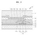
- FIG. 2 is a cross-sectional view illustrating a light emission unit 120 according to the embodiment of the present invention shown in FIG. 1 .
- an insulating layer 121 such as a barrier layer and/or a buffer layer may be formed on an upper surface of the first substrate 110 in order to prevent or reduce impurity ions from diffusing, to prevent or reduce humidity or external air from infiltrating in the first substrate 110, and/or to more closely planarize the upper surface of the first substrate 110.
- An active layer 122 of a thin film transistor (TFT) is formed on the insulating layer 121 by using one or more semiconductor materials, and a gate insulating layer 123 is formed on the first substrate 110 to cover the active layer 122.
- the active layer 122 may be formed of an inorganic semiconductor, such as amorphous silicon or polysilicon, or may be formed of an organic semiconductor.
- the active layer 122 has a source region 122a and a drain region 122b on two sides of a channel region 122c.
- a gate electrode 124 is formed on the gate insulating layer 123, and an interlayer dielectric 125 is formed on the gate insulating layer 123 to cover the gate electrode 124.
- a source electrode 126a and a drain electrode 126b are formed on the interlayer dielectric 125, and a planarization layer 127 and a pixel definition layer 128 are formed (e.g., sequentially formed in the order stated) to cover the source and drain electrodes 126a and 126b.
- the gate insulating layer 123, the interlayer dielectric 125, the planarization layer 127, and the pixel definition layer 128 may be formed of an insulating material, and may be formed in a single-layered structure or a multi-layered structure including an organic material, an inorganic material, and/or an organic/inorganic compound material.
- the present invention is not limited to the above-described stacked structure of the TFT, and TFTs having various structures may be used.
- a pixel electrode 129a which is an electrode included in an OLED, is formed on the planarization layer 127, and the pixel definition layer 128 is formed on the pixel electrode 129a. Furthermore, an opening (e.g., a predetermined opening) is formed in the pixel definition layer 128 to expose the pixel electrode 129a, and an organic emission layer 129b of the OLED is formed on the exposed portion of the pixel electrode 129a.
- the OLED may display image information (e.g., predetermined image information) by emitting red, green, or blue light according to the flow of electric current.
- the OLED includes the pixel electrode 129a that contacts the source electrode 126a of the TFT via a contact hole 127a formed in the planarization layer 127, an opposite electrode 129c located to cover all the pixels of the OLED, and the organic emission layer 129b located between the pixel electrode 129a and the opposite electrode 129c to emit light.
- the pixel electrode 129a and the opposite electrode 129c are insulated from each other by the organic emission layer 129b and may be used to apply voltages of different polarities to the organic emission layer 129b to make the organic emission layer 129b emit light.
- the organic emission layer 129b may be a low molecular weight organic film or a polymer organic film.
- the organic emission layer 129b may be formed by stacking a hole injection layer (HIL), a hole transport layer (HTL), an emission layer (EML), an electron transport layer (ETL), and an electron injection layer (EIL).
- HIL hole injection layer
- HTL hole transport layer
- EML emission layer
- ETL electron transport layer
- EIL electron injection layer
- the organic emission layer 129b may be formed in a single structure or a composite structure, and may be formed of any of various materials such as copper phthalocyanine (CuPc), N,N'-Di(naphthalene-1-yl)-N,N'-diphenyl-benzidine (NPB), or tris-8-hydroxyquinoline aluminum (Alq3). These layers may be formed by vacuum deposition.
- CuPc copper phthalocyanine
- NPB N,N'-Di(naphthalene-1-yl
- the HIL, the HTL, the ETL, and the EIL are common layers and may be commonly applied to red, green, and blue pixels. Accordingly, unlike the organic emission layer 129b in FIG. 2 , the common layers may be formed to cover all of the pixels, in a similar manner as, for example, the opposite electrode 129c.
- the pixel electrode 129a functions as an anode electrode
- the opposite electrode 129c functions as a cathode electrode.
- the present invention is not limited thereto, and the polarities of the pixel electrode 129a and the opposite electrode 129c may be reversed in other embodiments.
- the pixel electrode 129a may be a transparent electrode, and the opposite electrode 129c may be a reflection electrode.
- the pixel electrode 129a may be formed of an oxide having a high work function, such as indium tin oxide (ITO), indium zinc oxide (IZO), ZnO, or In 2 O 3
- the opposite electrode 129c may be formed of a metal having a low work function, such as, for example, silver (Ag), magnesium (Mg), aluminum (Al), platinum (Pt), palladium (Pd), gold (Au), nickel (Ni), neodymium (Nd), iridium (Ir), chromium (Cr), lithium (Li), or calcium (Ca).
- the pixel electrode 129a may be a reflection electrode, and the opposite electrode 129c may be a transparent electrode.
- the pixel electrode 129a may include a reflection film formed of Ag, Mg, Al, Pt, Pd, Au, Ni, Nd, Ir, Cr, Li, Ca, a compound of these materials, or an oxide having a high work function, such as, for example, ITO, IZO, ZnO, or In 2 O 3 .
- the opposite electrode 129c may be formed by first depositing a metal having a low work function, such as, for example, Ag, Mg, Al, Pt, Pd, Au, Ni, Nd, Ir, Cr, Li, Ca, or a compound of these materials, and then by forming an auxiliary electrode layer or a bus electrode line by using a transparent conductive material such as, for example, ITO, IZO, ZnO, or In 2 O 3 .
- a metal having a low work function such as, for example, Ag, Mg, Al, Pt, Pd, Au, Ni, Nd, Ir, Cr, Li, Ca, or a compound of these materials
- a transparent conductive material such as, for example, ITO, IZO, ZnO, or In 2 O 3 .
- both the pixel electrode 129a and the opposite electrode 129c may be formed as transparent electrodes.
- the OLED is a top emission type display, and the images may be displayed toward the second substrate 150.
- the OLED may be a bottom emission type display or a double emission type display.
- the materials of the pixel electrode 129a and the opposite electrode 129c are not limited to the above examples, and the pixel electrode 129a and the opposite electrode 129c may be formed of a conductive organic material or a conductive paste including conductive particles such as Ag, Mg, or Cu.
- a conductive paste including conductive particles such as Ag, Mg, or Cu.
- a passivation layer 10 composed of an inorganic material, an organic material, or an inorganic/organic compound material may be further formed on the opposite electrode 129c to cover the light emission unit 120.
- the present invention is not limited to the above-described formation, composition, or structure of the OLED and its corresponding components and layers, nor is the present invention limited to the above-described materials, as various displays of various structures and materials may be used.
- FIG. 3 is a top view illustrating the flat panel display 100 according to the embodiment of the present invention shown in FIG. 1 .
- the first sensing unit 130 and the second sensing unit 140 are located on the flat panel display 100 to measure intensities of light incident from outside of the flat panel display 100.
- the first and second sensing units 130 and 140 may be located on the non-emission region 111 of the first substrate 110.
- the non-emission region 111 may be a region corresponding to an outer portion of the emission region 112 and an inner portion of the bonding member 160.
- the first and second sensing units 130 and 140 may be symmetrically or substantially symmetrically arranged about the light emission unit 120.
- the first and second sensing units 130 and 140 are respectively located on a left non-emission region 111a and a right non-emission region 111b of the light emission unit 120, have substantially the same or identical heights, and are located symmetrically or substantially symmetrically about the light emission unit 120.
- the first and second sensing units 130 and 140 are located symmetrically or substantially symmetrically about the light emission unit 120, a difference between light intensities that may be generated if the first and second sensing units 130 and 140 are asymmetric with respect to each other may be reduced or prevented.
- external light may be incident on the first and second sensing units 130 and 140 under the same or similar conditions for each sensing unit 130 and 140, and variations in the intensities of incident light depending on the location and orientation of the first and second sensing units 130 and 140 may be reduced. It should be understood that the present invention is not limited to the above-mentioned locations of the sensing units 130 and 140, as different arrangements may be used.
- the first sensing unit 130 may include a first photosensor.
- the first photosensor 130 may be a PN junction optical diode and may include a first light receiving layer 131 and a second light receiving layer 132.
- the first light receiving layer 131 may be an N-type layer in the PN junction optical diode 130
- the second light receiving layer 132 may be a P-type layer in the PN junction optical diode 130.
- the first light receiving layer 131 may be a P-type layer in the PN junction optical diode 130
- the second light receiving layer 132 may be an N-type layer in the PN junction optical diode 130.
- the first light receiving layer 131 may include one or more elements selected from the group consisting of gallium (Ga), indium (In), zinc (Zn), and tin (Sn), and combined with oxygen (O).
- the first light receiving layer 131 may include ZnO, ZnGaO, ZnInO, GaInO, GaSnO, ZnSnO, InSnO, or ZnGaInO.
- the second light receiving layer 132 may include a phthalocyanine compound including one or more metals selected from the group consisting of Cu, Fe, Ni, Co, Mn, Al, Pd, Sn, In, Pb, Ti, Rb, V, Ga, Tb, Ce, La, and Zn.
- the first photosensor 130 may be a PIN junction optical diode.
- the second sensing unit 140 may include a second photosensor 141 and a light shielding member 142.
- the second photosensor 141 may be a PN junction optical diode.
- the second photosensor 141 may include a first light receiving layer 141a and a second light receiving layer 141b.
- the first light receiving layer 141a may be an N-type layer of the PN junction optical diode 141
- the second light receiving layer 141b may be a P-type layer of the PN junction optical diode 141.
- the first light receiving layer 141a may be a P-type layer of the PN junction optical diode 141
- the second light receiving layer 141 may be an N-type layer of the PN junction optical diode 141.
- the first light receiving layer 141a may include one or more selected from the group consisting of Ga, In, Zn, and Sn, and combined with O.
- the first light receiving layer 141a may include a material such as ZnO, ZnGaO, ZnInO, GaInO, GaSnO, ZnSnO, InSnO, or ZnGaInO.
- the second light receiving layer 141b may include a phthalocyanine compound including one or more metals selected from the group consisting of Cu, Fe, Ni, Co, Mn, Al, Pd, Sn, In, Pb, Ti, Rb, V, Ga, Tb, Ce, La, and Zn.
- the light shielding member 142 may be arranged to contact a side of the second photosensor 141. Furthermore, the light shielding member 142 may be arranged to contact an upper end portion of the second photosensor 141. However, the present invention is not limited thereto, and the light shielding member 142 may be arranged to contact other portions (e.g., sides) of the second photosensor 141 without contacting the upper end portion of the second photosensor 141. Furthermore, the light shielding member 142 may be arranged to not contact the second photosensor. Also, the light shielding member 142 may be pillar-shaped.
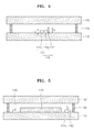
- FIG. 4 is a cross-sectional view illustrating the flat panel display 100 of the embodiment of the present invention shown in FIG. 1 and taken along the line I-I of FIG. 1
- FIG. 5 is a cross-sectional view illustrating the flat panel display 100 of the embodiment of the present invention shown in FIG. 1 and taken along the line II-II of FIG. 1 .
- the light shielding member 142 may have a width w1 that is less than a width w2 of the second photosensor 141, and may have a height t1 that is greater than a height t2 of the second photosensor 141.
- the light shielding member 142 may be formed with a height that is equal to or smaller than a height of the bonding member 160.
- the light shielding member 142 located on the side of the second photosensor 141 may reduce luminous flux of external light incident on the second photosensor 141. Accordingly, there may be a difference between the intensities of light incident on the first photosensor 130 and second photosensor 141, and thus, a tilt angle of the flat panel display 100 may be calculated by using such a difference. This will be described later in more detail.
- the present invention is not limited to the above-mentioned dimensions, locations, or orientations of the light shielding member 142, nor to the foregoing materials and arrangements, as they are provided merely as examples.
- FIG. 6 is a partial perspective view of a second sensing unit 140 of the flat panel display 100 according to another embodiment of the present invention.
- light shielding members 142a, 142b, 142c, and 142d may be respectively located at or near four sides of the second photosensor 141.
- the present invention is not limited thereto (e.g., at least one of the light shielding members 142a, 142b, 142c, and 142d may be located on or near a side of the second photosensor 141).
- By providing light shielding members at more than one side complex tilting of the flat panel display can be captured. In other words, tilting in more than one axis can be determined since, for example, first and second shielding members 142a, 142d provide for up and down tilting, while third and fourth shielding members 142c, 142d provide for side to side tilting.
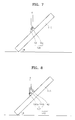
- FIGS. 7 and 8 are side views illustrating operations of the flat panel display 100 according to one embodiment of the present invention.
- FIG. 7 is a view of the flat panel display 100 seen from a side of the first sensing unit 130
- FIG. 8 is a view of the flat panel display 100 seen from a side of the second sensing unit 140, wherein the flat panel display 100 is tilted at a predetermined tilt angle ⁇ with respect to the ground.
- the flat panel display 100 is tilted (e.g., tilted with respect to the ground)
- some of the light proceeding toward the second photosensor 141 may be blocked by the light shielding member 142, so that it is not incident on the second photosensor 141.
- the light shielding member 142 may shield more light, the amount of light incident on the second photosensor 141 is then reduced, and the difference between the intensities of the light incident on the first photosensor 130 and on the second photosensor 141 becomes larger. It should be noted that although there is no light shielding member corresponding to the first photosensor 130 in the described embodiment, the present invention is not limited thereto.
- the intensity of the light incident on the first photosensor 130 is a first light intensity and the intensity of the light incident on the second photosensor 141 is a second light intensity
- the second light intensity may be reduced by the light shielding member 142 and a ratio of the second light intensity to the first light intensity decreases.
- the amount of light shielded by the light shielding member 142 is reduced, and a ratio of the second light intensity to the first light intensity increases.
- the first light intensity and the second light intensity may be equal or approximately equal to each other, and the ratio of the second light intensity to the first light intensity then approaches or becomes 1.
- the tilt angle of the flat panel display 100 may be calculated by measuring the first and second light intensities and calculating their ratio.
- the relations between the ratio of the second light intensity to the first light intensity, and/or its inverse (i.e., the ratio of the first light intensity with respect to the second light intensity), and the tilt angle of the flat panel display 100 may be listed in a look-up table and stored, and thus, the tilt angle of the flat panel display 100 may be calculated by measuring the first and second light intensities, calculating a ratio, and using the look-up table.
- the tilt angle of the flat panel display 100 may similarly by calculated to a reference other than the ground, and that the present invention is, therefore, not limited thereto.
- the tilt angle of the flat panel display 100 may be easily calculated using the first and second sensing units 130 and 140 in the absence of using an additional gyro sensor or a light intensity sensor.
Landscapes
- Physics & Mathematics (AREA)
- Nonlinear Science (AREA)
- Chemical & Material Sciences (AREA)
- General Physics & Mathematics (AREA)
- Optics & Photonics (AREA)
- Crystallography & Structural Chemistry (AREA)
- Mathematical Physics (AREA)
- Life Sciences & Earth Sciences (AREA)
- Inorganic Chemistry (AREA)
- Sustainable Development (AREA)
- Engineering & Computer Science (AREA)
- Computer Hardware Design (AREA)
- Theoretical Computer Science (AREA)
- Devices For Indicating Variable Information By Combining Individual Elements (AREA)
- Electroluminescent Light Sources (AREA)
Applications Claiming Priority (1)
| Application Number | Priority Date | Filing Date | Title |
|---|---|---|---|
| KR1020100023396A KR101074815B1 (ko) | 2010-03-16 | 2010-03-16 | 평판 디스플레이 장치 |
Publications (3)
| Publication Number | Publication Date |
|---|---|
| EP2378352A2 true EP2378352A2 (de) | 2011-10-19 |
| EP2378352A3 EP2378352A3 (de) | 2013-08-21 |
| EP2378352B1 EP2378352B1 (de) | 2017-07-19 |
Family
ID=44544046
Family Applications (1)
| Application Number | Title | Priority Date | Filing Date |
|---|---|---|---|
| EP11158336.5A Not-in-force EP2378352B1 (de) | 2010-03-16 | 2011-03-15 | Flachbildschirm |
Country Status (5)
| Country | Link |
|---|---|
| US (1) | US8730163B2 (de) |
| EP (1) | EP2378352B1 (de) |
| JP (1) | JP5623866B2 (de) |
| KR (1) | KR101074815B1 (de) |
| CN (1) | CN102194855B (de) |
Cited By (1)
| Publication number | Priority date | Publication date | Assignee | Title |
|---|---|---|---|---|
| KR102824933B1 (ko) * | 2024-12-31 | 2025-06-25 | 주식회사 원테이크 | 액정층을 포함하는 안티 글레어 미러 |
Families Citing this family (1)
| Publication number | Priority date | Publication date | Assignee | Title |
|---|---|---|---|---|
| JP6211688B2 (ja) * | 2015-08-31 | 2017-10-11 | Eizo株式会社 | 表示パネルモジュール、表示装置及び製造方法 |
Family Cites Families (17)
| Publication number | Priority date | Publication date | Assignee | Title |
|---|---|---|---|---|
| US4314546A (en) * | 1980-01-21 | 1982-02-09 | Rca Corporation | Array positioning system |
| US4672191A (en) * | 1984-06-19 | 1987-06-09 | Dennis Cofield | Shadow solar tracking device and system |
| JPH04254820A (ja) | 1991-02-06 | 1992-09-10 | Fujitsu Ltd | 液晶表示装置 |
| JPH1163981A (ja) * | 1997-08-25 | 1999-03-05 | Sony Corp | 光学式センサ |
| JP2002072963A (ja) * | 2000-06-12 | 2002-03-12 | Semiconductor Energy Lab Co Ltd | 発光モジュールおよびその駆動方法並びに光センサ |
| JP3840077B2 (ja) * | 2001-09-03 | 2006-11-01 | Tdk株式会社 | 光センサ及びそれを備えた表示装置 |
| US7026597B2 (en) * | 2003-04-09 | 2006-04-11 | Eastman Kodak Company | OLED display with integrated elongated photosensor |
| JP4409873B2 (ja) | 2003-08-21 | 2010-02-03 | シチズンホールディングス株式会社 | 表示装置 |
| KR20060026537A (ko) | 2004-09-21 | 2006-03-24 | 김동완 | 마이컴 제어를 이용한 디지털 조명제어시스템 |
| KR100689458B1 (ko) | 2005-07-08 | 2007-03-08 | 삼성전자주식회사 | 휴대단말기에서 표시부의 밝기조절 방법 |
| KR101256663B1 (ko) | 2005-12-28 | 2013-04-19 | 엘지디스플레이 주식회사 | 액정표시장치와 그의 제조 및 구동방법 |
| KR101284926B1 (ko) * | 2006-06-23 | 2013-07-10 | 엘지디스플레이 주식회사 | 액정표시장치와 그의 제조 및 구동방법 |
| JP2009092935A (ja) * | 2007-10-09 | 2009-04-30 | Toshiba Matsushita Display Technology Co Ltd | 表示装置及び表示装置の製造方法 |
| JP4571198B2 (ja) * | 2008-03-07 | 2010-10-27 | 京セラ株式会社 | 携帯通信端末 |
| JP4752922B2 (ja) * | 2009-01-30 | 2011-08-17 | ソニー株式会社 | 画像表示装置および電子装置 |
| JP5412868B2 (ja) * | 2009-02-23 | 2014-02-12 | エプソンイメージングデバイス株式会社 | 位置検出装置、電気光学装置及び電子機器 |
| JP2012068393A (ja) * | 2010-09-22 | 2012-04-05 | Mitsubishi Electric Corp | 表示装置 |
-
2010
- 2010-03-16 KR KR1020100023396A patent/KR101074815B1/ko not_active Expired - Fee Related
- 2010-10-22 JP JP2010237478A patent/JP5623866B2/ja not_active Expired - Fee Related
-
2011
- 2011-02-15 US US13/028,027 patent/US8730163B2/en active Active
- 2011-03-15 EP EP11158336.5A patent/EP2378352B1/de not_active Not-in-force
- 2011-03-15 CN CN201110064207.1A patent/CN102194855B/zh not_active Expired - Fee Related
Non-Patent Citations (1)
| Title |
|---|
| None |
Cited By (1)
| Publication number | Priority date | Publication date | Assignee | Title |
|---|---|---|---|---|
| KR102824933B1 (ko) * | 2024-12-31 | 2025-06-25 | 주식회사 원테이크 | 액정층을 포함하는 안티 글레어 미러 |
Also Published As
| Publication number | Publication date |
|---|---|
| US20110227888A1 (en) | 2011-09-22 |
| US8730163B2 (en) | 2014-05-20 |
| KR20110104315A (ko) | 2011-09-22 |
| KR101074815B1 (ko) | 2011-10-19 |
| EP2378352B1 (de) | 2017-07-19 |
| EP2378352A3 (de) | 2013-08-21 |
| CN102194855A (zh) | 2011-09-21 |
| JP2011191733A (ja) | 2011-09-29 |
| CN102194855B (zh) | 2015-09-30 |
| JP5623866B2 (ja) | 2014-11-12 |
Similar Documents
| Publication | Publication Date | Title |
|---|---|---|
| JP5240796B2 (ja) | 有機発光表示装置 | |
| US8854578B2 (en) | Display apparatus and method of operating the same | |
| US9099674B2 (en) | Organic light-emitting display device | |
| US8569762B2 (en) | Organic light-emitting display device having improved transmittance | |
| JP5969450B2 (ja) | 有機発光ディスプレイ装置および有機発光ディスプレイ装置の製造方法 | |
| US8421342B2 (en) | Organic light-emitting display device | |
| US7928431B2 (en) | Organic light emitting display apparatus | |
| US8797239B2 (en) | Organic light-emitting display device | |
| US20180151839A1 (en) | Organic light emitting display apparatus | |
| US8441182B2 (en) | Organic light emitting diode display | |
| US8541784B2 (en) | Organic light-emitting display | |
| US20110215329A1 (en) | Organic light-emitting display device | |
| KR20150059478A (ko) | 유기전계 발광소자 | |
| US9711576B2 (en) | Display, method of manufacturing display and electronic device | |
| US8461592B2 (en) | Organic light emitting display device | |
| KR20150066428A (ko) | 유기전계 발광소자 | |
| US9634072B2 (en) | Organic light-emitting display device and method of manufacturing the same | |
| EP2378352B1 (de) | Flachbildschirm | |
| KR101587822B1 (ko) | 유기전계발광 표시장치 및 그 제조 방법 | |
| US12238972B2 (en) | Display device | |
| JP2013080769A (ja) | 薄膜トランジスタならびに表示装置および電子機器 | |
| KR20130070301A (ko) | 유기전계 발광소자 |
Legal Events
| Date | Code | Title | Description |
|---|---|---|---|
| AK | Designated contracting states |
Kind code of ref document: A2 Designated state(s): AL AT BE BG CH CY CZ DE DK EE ES FI FR GB GR HR HU IE IS IT LI LT LU LV MC MK MT NL NO PL PT RO RS SE SI SK SM TR |
|
| AX | Request for extension of the european patent |
Extension state: BA ME |
|
| PUAI | Public reference made under article 153(3) epc to a published international application that has entered the european phase |
Free format text: ORIGINAL CODE: 0009012 |
|
| RAP1 | Party data changed (applicant data changed or rights of an application transferred) |
Owner name: SAMSUNG DISPLAY CO., LTD. |
|
| PUAL | Search report despatched |
Free format text: ORIGINAL CODE: 0009013 |
|
| AK | Designated contracting states |
Kind code of ref document: A3 Designated state(s): AL AT BE BG CH CY CZ DE DK EE ES FI FR GB GR HR HU IE IS IT LI LT LU LV MC MK MT NL NO PL PT RO RS SE SI SK SM TR |
|
| AX | Request for extension of the european patent |
Extension state: BA ME |
|
| RIC1 | Information provided on ipc code assigned before grant |
Ipc: G09G 3/34 20060101ALI20130718BHEP Ipc: G02F 1/133 20060101AFI20130718BHEP Ipc: H01L 27/32 20060101ALI20130718BHEP |
|
| 17P | Request for examination filed |
Effective date: 20131108 |
|
| RBV | Designated contracting states (corrected) |
Designated state(s): AL AT BE BG CH CY CZ DE DK EE ES FI FR GB GR HR HU IE IS IT LI LT LU LV MC MK MT NL NO PL PT RO RS SE SI SK SM TR |
|
| RAP1 | Party data changed (applicant data changed or rights of an application transferred) |
Owner name: SAMSUNG DISPLAY CO., LTD. |
|
| GRAP | Despatch of communication of intention to grant a patent |
Free format text: ORIGINAL CODE: EPIDOSNIGR1 |
|
| STAA | Information on the status of an ep patent application or granted ep patent |
Free format text: STATUS: GRANT OF PATENT IS INTENDED |
|
| RIC1 | Information provided on ipc code assigned before grant |
Ipc: H01L 27/32 20060101ALI20161221BHEP Ipc: G02F 1/133 20060101AFI20161221BHEP Ipc: G09G 3/34 20060101ALI20161221BHEP |
|
| INTG | Intention to grant announced |
Effective date: 20170119 |
|
| GRAS | Grant fee paid |
Free format text: ORIGINAL CODE: EPIDOSNIGR3 |
|
| GRAA | (expected) grant |
Free format text: ORIGINAL CODE: 0009210 |
|
| STAA | Information on the status of an ep patent application or granted ep patent |
Free format text: STATUS: THE PATENT HAS BEEN GRANTED |
|
| AK | Designated contracting states |
Kind code of ref document: B1 Designated state(s): AL AT BE BG CH CY CZ DE DK EE ES FI FR GB GR HR HU IE IS IT LI LT LU LV MC MK MT NL NO PL PT RO RS SE SI SK SM TR |
|
| REG | Reference to a national code |
Ref country code: GB Ref legal event code: FG4D |
|
| REG | Reference to a national code |
Ref country code: CH Ref legal event code: EP |
|
| REG | Reference to a national code |
Ref country code: IE Ref legal event code: FG4D |
|
| REG | Reference to a national code |
Ref country code: AT Ref legal event code: REF Ref document number: 910939 Country of ref document: AT Kind code of ref document: T Effective date: 20170815 |
|
| REG | Reference to a national code |
Ref country code: DE Ref legal event code: R096 Ref document number: 602011039629 Country of ref document: DE |
|
| REG | Reference to a national code |
Ref country code: NL Ref legal event code: MP Effective date: 20170719 |
|
| REG | Reference to a national code |
Ref country code: LT Ref legal event code: MG4D |
|
| REG | Reference to a national code |
Ref country code: AT Ref legal event code: MK05 Ref document number: 910939 Country of ref document: AT Kind code of ref document: T Effective date: 20170719 |
|
| PG25 | Lapsed in a contracting state [announced via postgrant information from national office to epo] |
Ref country code: LT Free format text: LAPSE BECAUSE OF FAILURE TO SUBMIT A TRANSLATION OF THE DESCRIPTION OR TO PAY THE FEE WITHIN THE PRESCRIBED TIME-LIMIT Effective date: 20170719 Ref country code: SE Free format text: LAPSE BECAUSE OF FAILURE TO SUBMIT A TRANSLATION OF THE DESCRIPTION OR TO PAY THE FEE WITHIN THE PRESCRIBED TIME-LIMIT Effective date: 20170719 Ref country code: AT Free format text: LAPSE BECAUSE OF FAILURE TO SUBMIT A TRANSLATION OF THE DESCRIPTION OR TO PAY THE FEE WITHIN THE PRESCRIBED TIME-LIMIT Effective date: 20170719 Ref country code: HR Free format text: LAPSE BECAUSE OF FAILURE TO SUBMIT A TRANSLATION OF THE DESCRIPTION OR TO PAY THE FEE WITHIN THE PRESCRIBED TIME-LIMIT Effective date: 20170719 Ref country code: NO Free format text: LAPSE BECAUSE OF FAILURE TO SUBMIT A TRANSLATION OF THE DESCRIPTION OR TO PAY THE FEE WITHIN THE PRESCRIBED TIME-LIMIT Effective date: 20171019 Ref country code: NL Free format text: LAPSE BECAUSE OF FAILURE TO SUBMIT A TRANSLATION OF THE DESCRIPTION OR TO PAY THE FEE WITHIN THE PRESCRIBED TIME-LIMIT Effective date: 20170719 Ref country code: FI Free format text: LAPSE BECAUSE OF FAILURE TO SUBMIT A TRANSLATION OF THE DESCRIPTION OR TO PAY THE FEE WITHIN THE PRESCRIBED TIME-LIMIT Effective date: 20170719 |
|
| REG | Reference to a national code |
Ref country code: FR Ref legal event code: PLFP Year of fee payment: 8 |
|
| PG25 | Lapsed in a contracting state [announced via postgrant information from national office to epo] |
Ref country code: LV Free format text: LAPSE BECAUSE OF FAILURE TO SUBMIT A TRANSLATION OF THE DESCRIPTION OR TO PAY THE FEE WITHIN THE PRESCRIBED TIME-LIMIT Effective date: 20170719 Ref country code: ES Free format text: LAPSE BECAUSE OF FAILURE TO SUBMIT A TRANSLATION OF THE DESCRIPTION OR TO PAY THE FEE WITHIN THE PRESCRIBED TIME-LIMIT Effective date: 20170719 Ref country code: RS Free format text: LAPSE BECAUSE OF FAILURE TO SUBMIT A TRANSLATION OF THE DESCRIPTION OR TO PAY THE FEE WITHIN THE PRESCRIBED TIME-LIMIT Effective date: 20170719 Ref country code: PL Free format text: LAPSE BECAUSE OF FAILURE TO SUBMIT A TRANSLATION OF THE DESCRIPTION OR TO PAY THE FEE WITHIN THE PRESCRIBED TIME-LIMIT Effective date: 20170719 Ref country code: BG Free format text: LAPSE BECAUSE OF FAILURE TO SUBMIT A TRANSLATION OF THE DESCRIPTION OR TO PAY THE FEE WITHIN THE PRESCRIBED TIME-LIMIT Effective date: 20171019 Ref country code: GR Free format text: LAPSE BECAUSE OF FAILURE TO SUBMIT A TRANSLATION OF THE DESCRIPTION OR TO PAY THE FEE WITHIN THE PRESCRIBED TIME-LIMIT Effective date: 20171020 Ref country code: IS Free format text: LAPSE BECAUSE OF FAILURE TO SUBMIT A TRANSLATION OF THE DESCRIPTION OR TO PAY THE FEE WITHIN THE PRESCRIBED TIME-LIMIT Effective date: 20171119 |
|
| REG | Reference to a national code |
Ref country code: DE Ref legal event code: R097 Ref document number: 602011039629 Country of ref document: DE |
|
| PG25 | Lapsed in a contracting state [announced via postgrant information from national office to epo] |
Ref country code: DK Free format text: LAPSE BECAUSE OF FAILURE TO SUBMIT A TRANSLATION OF THE DESCRIPTION OR TO PAY THE FEE WITHIN THE PRESCRIBED TIME-LIMIT Effective date: 20170719 Ref country code: RO Free format text: LAPSE BECAUSE OF FAILURE TO SUBMIT A TRANSLATION OF THE DESCRIPTION OR TO PAY THE FEE WITHIN THE PRESCRIBED TIME-LIMIT Effective date: 20170719 Ref country code: CZ Free format text: LAPSE BECAUSE OF FAILURE TO SUBMIT A TRANSLATION OF THE DESCRIPTION OR TO PAY THE FEE WITHIN THE PRESCRIBED TIME-LIMIT Effective date: 20170719 |
|
| PLBE | No opposition filed within time limit |
Free format text: ORIGINAL CODE: 0009261 |
|
| STAA | Information on the status of an ep patent application or granted ep patent |
Free format text: STATUS: NO OPPOSITION FILED WITHIN TIME LIMIT |
|
| PG25 | Lapsed in a contracting state [announced via postgrant information from national office to epo] |
Ref country code: SM Free format text: LAPSE BECAUSE OF FAILURE TO SUBMIT A TRANSLATION OF THE DESCRIPTION OR TO PAY THE FEE WITHIN THE PRESCRIBED TIME-LIMIT Effective date: 20170719 Ref country code: SK Free format text: LAPSE BECAUSE OF FAILURE TO SUBMIT A TRANSLATION OF THE DESCRIPTION OR TO PAY THE FEE WITHIN THE PRESCRIBED TIME-LIMIT Effective date: 20170719 Ref country code: IT Free format text: LAPSE BECAUSE OF FAILURE TO SUBMIT A TRANSLATION OF THE DESCRIPTION OR TO PAY THE FEE WITHIN THE PRESCRIBED TIME-LIMIT Effective date: 20170719 Ref country code: EE Free format text: LAPSE BECAUSE OF FAILURE TO SUBMIT A TRANSLATION OF THE DESCRIPTION OR TO PAY THE FEE WITHIN THE PRESCRIBED TIME-LIMIT Effective date: 20170719 |
|
| 26N | No opposition filed |
Effective date: 20180420 |
|
| PG25 | Lapsed in a contracting state [announced via postgrant information from national office to epo] |
Ref country code: SI Free format text: LAPSE BECAUSE OF FAILURE TO SUBMIT A TRANSLATION OF THE DESCRIPTION OR TO PAY THE FEE WITHIN THE PRESCRIBED TIME-LIMIT Effective date: 20170719 |
|
| REG | Reference to a national code |
Ref country code: CH Ref legal event code: PL |
|
| PG25 | Lapsed in a contracting state [announced via postgrant information from national office to epo] |
Ref country code: MC Free format text: LAPSE BECAUSE OF FAILURE TO SUBMIT A TRANSLATION OF THE DESCRIPTION OR TO PAY THE FEE WITHIN THE PRESCRIBED TIME-LIMIT Effective date: 20170719 |
|
| REG | Reference to a national code |
Ref country code: BE Ref legal event code: MM Effective date: 20180331 |
|
| REG | Reference to a national code |
Ref country code: IE Ref legal event code: MM4A |
|
| PG25 | Lapsed in a contracting state [announced via postgrant information from national office to epo] |
Ref country code: LU Free format text: LAPSE BECAUSE OF NON-PAYMENT OF DUE FEES Effective date: 20180315 |
|
| PG25 | Lapsed in a contracting state [announced via postgrant information from national office to epo] |
Ref country code: IE Free format text: LAPSE BECAUSE OF NON-PAYMENT OF DUE FEES Effective date: 20180315 |
|
| PG25 | Lapsed in a contracting state [announced via postgrant information from national office to epo] |
Ref country code: LI Free format text: LAPSE BECAUSE OF NON-PAYMENT OF DUE FEES Effective date: 20180331 Ref country code: CH Free format text: LAPSE BECAUSE OF NON-PAYMENT OF DUE FEES Effective date: 20180331 Ref country code: BE Free format text: LAPSE BECAUSE OF NON-PAYMENT OF DUE FEES Effective date: 20180331 |
|
| PGFP | Annual fee paid to national office [announced via postgrant information from national office to epo] |
Ref country code: DE Payment date: 20190305 Year of fee payment: 9 Ref country code: FR Payment date: 20190307 Year of fee payment: 9 Ref country code: GB Payment date: 20190306 Year of fee payment: 9 |
|
| PG25 | Lapsed in a contracting state [announced via postgrant information from national office to epo] |
Ref country code: MT Free format text: LAPSE BECAUSE OF NON-PAYMENT OF DUE FEES Effective date: 20180315 |
|
| PG25 | Lapsed in a contracting state [announced via postgrant information from national office to epo] |
Ref country code: TR Free format text: LAPSE BECAUSE OF FAILURE TO SUBMIT A TRANSLATION OF THE DESCRIPTION OR TO PAY THE FEE WITHIN THE PRESCRIBED TIME-LIMIT Effective date: 20170719 |
|
| PG25 | Lapsed in a contracting state [announced via postgrant information from national office to epo] |
Ref country code: PT Free format text: LAPSE BECAUSE OF FAILURE TO SUBMIT A TRANSLATION OF THE DESCRIPTION OR TO PAY THE FEE WITHIN THE PRESCRIBED TIME-LIMIT Effective date: 20170719 Ref country code: HU Free format text: LAPSE BECAUSE OF FAILURE TO SUBMIT A TRANSLATION OF THE DESCRIPTION OR TO PAY THE FEE WITHIN THE PRESCRIBED TIME-LIMIT; INVALID AB INITIO Effective date: 20110315 |
|
| PG25 | Lapsed in a contracting state [announced via postgrant information from national office to epo] |
Ref country code: MK Free format text: LAPSE BECAUSE OF NON-PAYMENT OF DUE FEES Effective date: 20170719 Ref country code: CY Free format text: LAPSE BECAUSE OF FAILURE TO SUBMIT A TRANSLATION OF THE DESCRIPTION OR TO PAY THE FEE WITHIN THE PRESCRIBED TIME-LIMIT Effective date: 20170719 |
|
| PG25 | Lapsed in a contracting state [announced via postgrant information from national office to epo] |
Ref country code: AL Free format text: LAPSE BECAUSE OF FAILURE TO SUBMIT A TRANSLATION OF THE DESCRIPTION OR TO PAY THE FEE WITHIN THE PRESCRIBED TIME-LIMIT Effective date: 20170719 |
|
| REG | Reference to a national code |
Ref country code: DE Ref legal event code: R119 Ref document number: 602011039629 Country of ref document: DE |
|
| PG25 | Lapsed in a contracting state [announced via postgrant information from national office to epo] |
Ref country code: FR Free format text: LAPSE BECAUSE OF NON-PAYMENT OF DUE FEES Effective date: 20200331 Ref country code: DE Free format text: LAPSE BECAUSE OF NON-PAYMENT OF DUE FEES Effective date: 20201001 |
|
| GBPC | Gb: european patent ceased through non-payment of renewal fee |
Effective date: 20200315 |
|
| PG25 | Lapsed in a contracting state [announced via postgrant information from national office to epo] |
Ref country code: GB Free format text: LAPSE BECAUSE OF NON-PAYMENT OF DUE FEES Effective date: 20200315 |