EP2378538A2 - Cathode annulaire pour une utilisation dans un dispositif de pulvérisation de magnétron - Google Patents
Cathode annulaire pour une utilisation dans un dispositif de pulvérisation de magnétron Download PDFInfo
- Publication number
- EP2378538A2 EP2378538A2 EP11162661A EP11162661A EP2378538A2 EP 2378538 A2 EP2378538 A2 EP 2378538A2 EP 11162661 A EP11162661 A EP 11162661A EP 11162661 A EP11162661 A EP 11162661A EP 2378538 A2 EP2378538 A2 EP 2378538A2
- Authority
- EP
- European Patent Office
- Prior art keywords
- cathode
- magnetron sputtering
- radius
- sputtering device
- anode
- Prior art date
- Legal status (The legal status is an assumption and is not a legal conclusion. Google has not performed a legal analysis and makes no representation as to the accuracy of the status listed.)
- Granted
Links
Images




Classifications
-
- C—CHEMISTRY; METALLURGY
- C23—COATING METALLIC MATERIAL; COATING MATERIAL WITH METALLIC MATERIAL; CHEMICAL SURFACE TREATMENT; DIFFUSION TREATMENT OF METALLIC MATERIAL; COATING BY VACUUM EVAPORATION, BY SPUTTERING, BY ION IMPLANTATION OR BY CHEMICAL VAPOUR DEPOSITION, IN GENERAL; INHIBITING CORROSION OF METALLIC MATERIAL OR INCRUSTATION IN GENERAL
- C23C—COATING METALLIC MATERIAL; COATING MATERIAL WITH METALLIC MATERIAL; SURFACE TREATMENT OF METALLIC MATERIAL BY DIFFUSION INTO THE SURFACE, BY CHEMICAL CONVERSION OR SUBSTITUTION; COATING BY VACUUM EVAPORATION, BY SPUTTERING, BY ION IMPLANTATION OR BY CHEMICAL VAPOUR DEPOSITION, IN GENERAL
- C23C14/00—Coating by vacuum evaporation, by sputtering or by ion implantation of the coating forming material
- C23C14/22—Coating by vacuum evaporation, by sputtering or by ion implantation of the coating forming material characterised by the process of coating
- C23C14/34—Sputtering
- C23C14/35—Sputtering by application of a magnetic field, e.g. magnetron sputtering
-
- C—CHEMISTRY; METALLURGY
- C23—COATING METALLIC MATERIAL; COATING MATERIAL WITH METALLIC MATERIAL; CHEMICAL SURFACE TREATMENT; DIFFUSION TREATMENT OF METALLIC MATERIAL; COATING BY VACUUM EVAPORATION, BY SPUTTERING, BY ION IMPLANTATION OR BY CHEMICAL VAPOUR DEPOSITION, IN GENERAL; INHIBITING CORROSION OF METALLIC MATERIAL OR INCRUSTATION IN GENERAL
- C23C—COATING METALLIC MATERIAL; COATING MATERIAL WITH METALLIC MATERIAL; SURFACE TREATMENT OF METALLIC MATERIAL BY DIFFUSION INTO THE SURFACE, BY CHEMICAL CONVERSION OR SUBSTITUTION; COATING BY VACUUM EVAPORATION, BY SPUTTERING, BY ION IMPLANTATION OR BY CHEMICAL VAPOUR DEPOSITION, IN GENERAL
- C23C14/00—Coating by vacuum evaporation, by sputtering or by ion implantation of the coating forming material
- C23C14/0021—Reactive sputtering or evaporation
- C23C14/0036—Reactive sputtering
-
- C—CHEMISTRY; METALLURGY
- C23—COATING METALLIC MATERIAL; COATING MATERIAL WITH METALLIC MATERIAL; CHEMICAL SURFACE TREATMENT; DIFFUSION TREATMENT OF METALLIC MATERIAL; COATING BY VACUUM EVAPORATION, BY SPUTTERING, BY ION IMPLANTATION OR BY CHEMICAL VAPOUR DEPOSITION, IN GENERAL; INHIBITING CORROSION OF METALLIC MATERIAL OR INCRUSTATION IN GENERAL
- C23C—COATING METALLIC MATERIAL; COATING MATERIAL WITH METALLIC MATERIAL; SURFACE TREATMENT OF METALLIC MATERIAL BY DIFFUSION INTO THE SURFACE, BY CHEMICAL CONVERSION OR SUBSTITUTION; COATING BY VACUUM EVAPORATION, BY SPUTTERING, BY ION IMPLANTATION OR BY CHEMICAL VAPOUR DEPOSITION, IN GENERAL
- C23C14/00—Coating by vacuum evaporation, by sputtering or by ion implantation of the coating forming material
- C23C14/22—Coating by vacuum evaporation, by sputtering or by ion implantation of the coating forming material characterised by the process of coating
- C23C14/34—Sputtering
- C23C14/3407—Cathode assembly for sputtering apparatus, e.g. Target
-
- C—CHEMISTRY; METALLURGY
- C23—COATING METALLIC MATERIAL; COATING MATERIAL WITH METALLIC MATERIAL; CHEMICAL SURFACE TREATMENT; DIFFUSION TREATMENT OF METALLIC MATERIAL; COATING BY VACUUM EVAPORATION, BY SPUTTERING, BY ION IMPLANTATION OR BY CHEMICAL VAPOUR DEPOSITION, IN GENERAL; INHIBITING CORROSION OF METALLIC MATERIAL OR INCRUSTATION IN GENERAL
- C23C—COATING METALLIC MATERIAL; COATING MATERIAL WITH METALLIC MATERIAL; SURFACE TREATMENT OF METALLIC MATERIAL BY DIFFUSION INTO THE SURFACE, BY CHEMICAL CONVERSION OR SUBSTITUTION; COATING BY VACUUM EVAPORATION, BY SPUTTERING, BY ION IMPLANTATION OR BY CHEMICAL VAPOUR DEPOSITION, IN GENERAL
- C23C14/00—Coating by vacuum evaporation, by sputtering or by ion implantation of the coating forming material
- C23C14/22—Coating by vacuum evaporation, by sputtering or by ion implantation of the coating forming material characterised by the process of coating
- C23C14/50—Substrate holders
- C23C14/505—Substrate holders for rotation of the substrates
-
- H—ELECTRICITY
- H01—ELECTRIC ELEMENTS
- H01J—ELECTRIC DISCHARGE TUBES OR DISCHARGE LAMPS
- H01J37/00—Discharge tubes with provision for introducing objects or material to be exposed to the discharge, e.g. for the purpose of examination or processing thereof
- H01J37/32—Gas-filled discharge tubes
- H01J37/34—Gas-filled discharge tubes operating with cathodic sputtering
- H01J37/3402—Gas-filled discharge tubes operating with cathodic sputtering using supplementary magnetic fields
- H01J37/3405—Magnetron sputtering
-
- H—ELECTRICITY
- H01—ELECTRIC ELEMENTS
- H01J—ELECTRIC DISCHARGE TUBES OR DISCHARGE LAMPS
- H01J37/00—Discharge tubes with provision for introducing objects or material to be exposed to the discharge, e.g. for the purpose of examination or processing thereof
- H01J37/32—Gas-filled discharge tubes
- H01J37/34—Gas-filled discharge tubes operating with cathodic sputtering
- H01J37/3411—Constructional aspects of the reactor
- H01J37/3414—Targets
- H01J37/3417—Arrangements
-
- H—ELECTRICITY
- H01—ELECTRIC ELEMENTS
- H01J—ELECTRIC DISCHARGE TUBES OR DISCHARGE LAMPS
- H01J37/00—Discharge tubes with provision for introducing objects or material to be exposed to the discharge, e.g. for the purpose of examination or processing thereof
- H01J37/32—Gas-filled discharge tubes
- H01J37/34—Gas-filled discharge tubes operating with cathodic sputtering
- H01J37/3411—Constructional aspects of the reactor
- H01J37/3414—Targets
- H01J37/3423—Shape
-
- H—ELECTRICITY
- H01—ELECTRIC ELEMENTS
- H01J—ELECTRIC DISCHARGE TUBES OR DISCHARGE LAMPS
- H01J37/00—Discharge tubes with provision for introducing objects or material to be exposed to the discharge, e.g. for the purpose of examination or processing thereof
- H01J37/32—Gas-filled discharge tubes
- H01J37/34—Gas-filled discharge tubes operating with cathodic sputtering
- H01J37/3411—Constructional aspects of the reactor
- H01J37/3438—Electrodes other than cathode
-
- H—ELECTRICITY
- H01—ELECTRIC ELEMENTS
- H01J—ELECTRIC DISCHARGE TUBES OR DISCHARGE LAMPS
- H01J37/00—Discharge tubes with provision for introducing objects or material to be exposed to the discharge, e.g. for the purpose of examination or processing thereof
- H01J37/32—Gas-filled discharge tubes
- H01J37/34—Gas-filled discharge tubes operating with cathodic sputtering
- H01J37/3464—Operating strategies
- H01J37/347—Thickness uniformity of coated layers or desired profile of target erosion
-
- H—ELECTRICITY
- H10—SEMICONDUCTOR DEVICES; ELECTRIC SOLID-STATE DEVICES NOT OTHERWISE PROVIDED FOR
- H10P—GENERIC PROCESSES OR APPARATUS FOR THE MANUFACTURE OR TREATMENT OF DEVICES COVERED BY CLASS H10
- H10P72/00—Handling or holding of wafers, substrates or devices during manufacture or treatment thereof
- H10P72/70—Handling or holding of wafers, substrates or devices during manufacture or treatment thereof for supporting or gripping
- H10P72/76—Handling or holding of wafers, substrates or devices during manufacture or treatment thereof for supporting or gripping using mechanical means, e.g. clamps or pinches
- H10P72/7604—Handling or holding of wafers, substrates or devices during manufacture or treatment thereof for supporting or gripping using mechanical means, e.g. clamps or pinches the wafers being placed on a susceptor, stage or support
- H10P72/7618—Handling or holding of wafers, substrates or devices during manufacture or treatment thereof for supporting or gripping using mechanical means, e.g. clamps or pinches the wafers being placed on a susceptor, stage or support characterised by a movable susceptor, stage or support, others than those only rotating on their own vertical axis, e.g. susceptors on a rotating carrousel
-
- H—ELECTRICITY
- H10—SEMICONDUCTOR DEVICES; ELECTRIC SOLID-STATE DEVICES NOT OTHERWISE PROVIDED FOR
- H10P—GENERIC PROCESSES OR APPARATUS FOR THE MANUFACTURE OR TREATMENT OF DEVICES COVERED BY CLASS H10
- H10P72/00—Handling or holding of wafers, substrates or devices during manufacture or treatment thereof
- H10P72/70—Handling or holding of wafers, substrates or devices during manufacture or treatment thereof for supporting or gripping
- H10P72/76—Handling or holding of wafers, substrates or devices during manufacture or treatment thereof for supporting or gripping using mechanical means, e.g. clamps or pinches
- H10P72/7604—Handling or holding of wafers, substrates or devices during manufacture or treatment thereof for supporting or gripping using mechanical means, e.g. clamps or pinches the wafers being placed on a susceptor, stage or support
- H10P72/7621—Handling or holding of wafers, substrates or devices during manufacture or treatment thereof for supporting or gripping using mechanical means, e.g. clamps or pinches the wafers being placed on a susceptor, stage or support characterised by supporting two or more semiconductor substrates
Definitions
- This invention relates generally to a magnetron sputtering device for depositing materials onto substrates in which the deposited films have a predictive thickness distribution with low defect levels. More particularly the invention relates to a ring cathode for use in a magnetron sputtering device and a magnetron sputtering device incorporating the same.
- Sputter coating is a widely used technique for depositing a thin film of material on a substrate.
- ions are usually created by collisions between gas atoms and electrons in a glow discharge.
- the ions are accelerated into the target of coating material at the cathode by an electric field causing atoms of the target material to be ejected from the target surface.
- a substrate is placed in a suitable location so that it intercepts a portion of the ejected atoms.
- a coating of target material is deposited on the surface of the substrate.
- a gaseous species is also present at the substrate surface and reacts with, and in some embodiments combines with, the atoms from the target surface to form the desired coating material.
- sputter gas e.g. argon
- a DC voltage applied between the cathode and the anode ionizes the argon into a plasma, and the positively charged argon ions are attracted to the negatively charged cathode.
- the ions strike the target in front of the cathode with a substantial energy and cause target atoms or atomic clusters to be sputtered from the target. Some of the target particles strike and deposit on the wafer or substrate material to be coated, thereby forming a film.
- the cathode includes an array of permanent magnets arranged in a closed loop and mounted in a fixed position in relation to the flat target plate of coating material.
- the magnetic field causes the electrons to travel in a closed loop, commonly referred to as a "race track", which establishes the path or region along which sputtering or erosion of the target material takes place.
- a magnetic field confines the glow discharge plasma and increases the path length of the electrons moving under the influence of the electric field. This results in an increase in the gas atom-electron collision probability, thereby leading to a much higher sputtering rate than that obtained without the use of magnetic confinement. Furthermore, the sputtering process can be accomplished at a much lower gas pressure.
- a magnetron sputtering system is operated at a pressure of 2* 10 ⁇ -2 Pa-1*10 ⁇ -1 Pa. during sputtering.
- the chamber is pumped down to a pressure of ⁇ 1*10 ⁇ -4 and a controlled flow of a gas, typically Argon (and in case of reactive sputtering Argon and Oxygen) is fed into the chamber to maintain the desired pressure.
- a gas typically Argon (and in case of reactive sputtering Argon and Oxygen) is fed into the chamber to maintain the desired pressure.
- a pressure of>2Pa. is required to be able to ignite and sustain a plasma.
- High pressure has the disadvantage that the mean-free path is greatly reduced, which causes extensive gas scatter. This results in hazy coatings.
- Cathode geometry particularly the relationship between the cathode shape, position and dimensions and the objects to be coated, has a significant effect on the rate of deposition and the area coated, as well as product quality and consistency.
- Variation in layer thickness across a substrate is referred to as runoff.
- the runoff can be predicted through modeling. It is desired to provide good film thickness uniformity, low runoff, over large diameter substrates.
- the anode provides a charge differential to the negatively charged cathode. This can be provided as simply as an electric charge provided to the chamber walls. However, the sputtered material is also deposited on any surface exposed to the sputtered atoms. If the coating is an electrically insulating material, such as a metal oxide, the build up of the material on other parts of the sputtering apparatus can cause problems. In particular, the build up of an insulating coating on the anode interferes with the ability of the anode to remove electrons from the plasma, as required to maintain the plasma's charge balance. This destabilizes the plasma and interferes with deposition control. Coating build-up will cause the anode location to move to another surface in the system. This instability affects coating quality.
- An increase coating capacity can be realized through an increase in deposition rates or an increase in load size, or both.
- To increase deposition rates it is necessary to increase the power density at the target.
- higher power density leads to an increase in arcing and in some targets, such as silicon, to an increase in target cracking.
- a larger target allows a higher material removal rate without increasing the power density.
- Greater efficiency of oxidation of the deposited film can also increase the deposition rate for reactive sputtering. Maintaining runoff limits is a challenge to increasing load size. In a concentric system where the cathode and planetary drive share a common center point, enlarging the planetary drive system for larger or a greater number of substrates requires an increase in throw distance.
- the present invention has found a ring cathode geometry that increases coating area and target material efficiency in a magnetron sputtering device with a planetary drive system, where the cathode axis is offset to the planetary drive.
- the ring cathode geometry and the off-center double rotation system for the substrates allows the realization of excellent coating uniformity across large substrates without the use of masking. Low defect levels are maintained by lowering power density on the cathode.
- the invention provides a magnetron sputtering device including:
- the invention further comprises a magnetron sputtering device for providing a sputter coating to a substrate without the use of a mask.
- the magnetron sputtering device described above further includes an activated source for a reactive gas.
- the activated source for a reactive gas is located at the center of the ring shaped cathode.
- the magnetron sputtering device further includes an anode for providing a voltage difference to the cathode, such that the anode is the preferred return path for electrons.
- the anode comprises an interior conductive surface of a vessel having an insulated outer surface electrically isolated from the chamber walls.
- the vessel has an opening in communication with a chamber interior, the opening being significantly smaller than a circumference of the vessel to shield the interior conductive surface from most sputtered material.
- a source for sputtering gas is coupled into the vessel for providing sputtering gas through the opening into the chamber, and the opening is dimensioned to permit a flow of gas to increase the pressure locally within the anode vessel above the pressure of the evacuated chamber.
- the magnetron sputtering device including the anode described above further includes an activated source for a reactive gas.
- the anode including a source for sputtering gas is located such that the opening of the vessel in communication with the chamber interior is at the center of the ring shaped cathode.
- the invention further includes the magnetron sputtering device including an activated source for reactive gas, wherein the anode is located such that the opening of the vessel in communication with the chamber interior is at the center of the ring shaped cathode.
- the invention further includes the magnetron sputtering device including the anode as a source for sputtering gas, wherein the activated source for a reactive gas is located at the center of the ring shaped cathode.
- the magnetron sputtering device including the anode as a source for sputtering gas, wherein the anode further includes a source for a reactive gas coupled into the vessel for providing an activated reactive gas together with the sputtering gas through the opening into the chamber.
- the magnetron sputtering device above including the anode as a source for sputtering gas and a reactive gas, wherein the opening into the chamber of the vessel comprising the anode is located at the center of the ring shaped cathode.
- the magnetron sputtering device above including the anode as a source for sputtering gas and a reactive gas located at the center of the ring shaped cathode, further including an auxiliary activated reactive source located a distance from the cathode.
- the magnetron sputtering device includes the cathode radius r1/r2 wherein 0.95*r2 > r1 > 0.6*r2.
- the cathode diameter r2 is equal to or larger than1.11 times the planet radius (r2> 1.11 * r W ).
- the magnetron sputtering device as defined above further includes within the chamber one or more alternate ring shaped cathode including a ring shaped target comprising material for forming a coating, wherein the offset distance r T is greater than one times the outer radius r2 (r T >1 *r2).
- the present invention increases coating uniformity in both runoff and planet to planet results over the prior art. Tolerance to mechanical deviation in vertical and horizontal positioning is significantly relaxed. Thus with close mechanical control significant improvement in planet to planet uniformity can be achieved. This quality control can be maintained over relatively large substrates (300mm) and despite scale up for increased load, while still maintaining a relatively short throw distance. In accordance with the present invention this uniformity can be achieved without the use of a mask.
- FIG. 1 An isometric view of the coating chamber 2 of the magnetron sputter coating device 10 is shown in Fig. 1 .
- Pumps 8 evacuate the coating chamber 2 for operation under vacuum conditions, understood to mean where the pressure is below atmospheric pressure.
- the chamber walls 32 are grounded and isolated from the positively charged anode 20 and the negatively charged cathode 12.
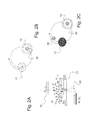
- a planetary drive 14, seen in more detail in Figs. 3A and 3B comprises a carrier 16 or rack rotatable about a central rotational axis C, with a plurality of eg. seven or eight, planets 17 supported radially about the central rotational axis C.
- a carrier radius r c is defined between the central axis C and the planet axis Cs.
- a ring shaped cathode 12, in this embodiment two cathodes 12, are shown each having a central axis Cc that is offset from the central axis C of the planetary drive 14.
- Anode 20, in the form of a vessel with an opening in communication with the coating chamber 2, is shielded from coating material and averted from a direct line to the target material of the cathode 12.
- An activated reactive gas source 36 is shown at the center of cathode 12. These positions can be reversed with 36 comprising an anode at the center of the cathode 12 and an activated reactive source 20 disposed a distance from the cathode 12.
- a preferred location for a reactive source 36 is at a radial position r C from C. as seen in Fig.
- FIG. 2C An alternative embodiment is shown in Fig. 2A and 2B in which the anode vessel 20' is positioned in the center of the ring cathode 12 functioning also as the source of reactive gas. If the anode 20' is a source of activated reactive gas at the center of the cathode (36 in Fig. 1 ), an auxiliary activated oxygen source can be located at 20 in Fig. 1 , to enable a higher deposition rate.
- the magnetron sputter coating device 10 includes a load lock 1 for loading and unloading substrates or other objects 23, for coating. This allows the deposition chamber 2 to remain under vacuum conditions at all times.
- the device is depicted here in the sputter up configuration. However, the geometry of the present invention applies equally to a sputter down, horizontal, or other orientation.
- Pulsed DC magnetron sputtering is the preferred process.
- the invention can also be implemented in DC magnetron, AC magnetron sputtering and rf magnetron sputtering.
- optical coatings have discriminating features in their spectral response.
- an edge filter for color separation lets one color pass while rejecting other colors.
- the precision requirement across a whole 200 mm or 300 mm substrate for the coating is assumed to be 0.5%.
- the edge were at 500 nm, this would translate to a 2.5 nm absolute edge placement variation.
- the placement of the spectral feature is related to the thickness of the layers in the coating design.
- the variation in coating rates across the substrate needs to be below 0.5%. If multiple substrates are coated in the same batch, the variation from one substrate to another needs to be a fraction of that.
- the variation in placement of a spectral feature is also referred to as runoff.
- the planetary drive 14 and ring cathode 12 are shown schematically in greater detail in Figs. 3A and 3B .
- the planetary drive 14 includes a central axis C about which the drive system rotates, and a plurality of secondary axes Cs, about which each planet 17 rotates independently.
- the distance between the central axis C and secondary axes Cs is a carrier radius r c .
- Each planet 17 has a radius r w that defines a largest usable coating area.
- the number and size of planets 17 desired determines the size of the planetary drive 14 and the capacity of the device 10.
- the planets 17 in a planetary coating geometry are supported at a common distance r c from the central rotational axis C.
- Each planet 17 can support single or a plurality of substrates, optical prisms, lenses or other objects 23.
- the object 23 to be coated can comprise a plurality of smaller separated parts mounted on a support substrate.
- the planet radius r w merely defines the usable coating area for each planet 17.
- a planet 17 in structure need not be this dimension itself, but is able to support a substrate 23 of this radius, or multiple objects 23 to be coated within this area.
- large objects such as bulk optics may have a thickness of up to 32 mm. With controlled height adjustment, a well defined target surface to object surface distance results in minimum runoff.
- Independent planet rotation may comprise a coordinated rotation rate relative to the rotation about the central rotational axis C.
- the secondary axes Cs are preferably parallel to the central rotational axis C, but may be at some other angle.
- Each planet 17 is disposed to experience substantially the same conditions as every other planet 17.
- an object plane 46 is illustrated at the coating surface of the substrates or other objects 23.
- a throw distance h is measured between the object plane 46 and the target surface plane 44 of the cathode 12.
- the ring cathode 12 has a large radius r2, larger than the planet radius r w .
- the cathode radius r2 can be optimized to maintain a required runoff.
- One other factor is the ring width.
- the cathode has an inner radius r1. The narrower the ring is, that is the larger r1/r2, the larger the rack or substrate 17 can be to achieve the same uniformity.
- a larger cathode radius requires a lower power density to achieve high deposition rates, despite a high total power in the cathode 12. This minimizes charge buildup on the target 24 and resultant arcing.
- the central axis Cc of the cathode 12 is translated an offset distance r T from the central axis C.
- This translation or offset distance r T is equal to between 2/3 and 4/3 the carrier radius, r c .
- the offset distance is varied in dependence on the substrate size or number of substrates to be coated.
- the cathode 12 has an inner radius r1 and an outer radius r2, measured at the erosion zone of the target, shown clearly in Fig. 4B . Together these radii define a preferably narrow ring. Both the cathode 12 and the target 24 of coating material have substantially the same annular ring shape and dimension.
- An inner radius can be as large as 0.98*r2, and should be at least 0.25*r2. While improved results are seen at 0.55*r2. For a 300mm substrate an optimum runoff is achieved with a narrow cathode ring of r1/r2 of 0.70 or larger.
- the outer radius r2 is dependent on the radius r w of the planets 17.
- the radius r2 is greater than the planet radius (r2>r w ) and ideally is 2 times the radius of the planet 17.
- the cathode radius can be larger than r2>2*r w though this depends on space limitations in the chamber.
- a larger radius (r2) ring cathode results in better coating uniformity when comparing rings of equal width (eg. r2 - r1). This can be seen in Figure 6 . It is important to note that a large target by itself does not necessarily result in good uniformity. Simulation shows that circular (non-annular) high utilization cathodes result in poor uniformity. Simulation data is shown in Fig. 6 .
- the performance of the geometry of the present invention had been predicted through numerical modeling.
- the large ring cathode 12 includes an inner magnetic ring 35 and an outer magnetic ring 37.
- the ring target can be described as having an inner and outer racetrack radius.
- the racetrack of a magnetron cathode describes the area over which material is ejected.
- the main contributor to this pattern is the horizontal magnetic field strength in front of the target 24.
- the magnetic field is generated by the permanent magnets 35, 37 in two concentric rings below the target.
- the inner magnetic ring 35 having a radius substantially equal or smaller than r1, and the outer magnetic ring having a radius substantially equal or larger than r2.
- the two magnetic rings 35,37 have opposing polarity with their axes perpendicular to the surface 44 of the target 24.. Due to the relatively narrow ring, high magnetic fields can be achieved which lead to low target voltage (between -250V and -650 V) and usually to lower stress in the deposited layers.
- the cathode can be driven with any electrical mode, eg. RF, DC, pulsed DC, MF, dual cathode-AC, single cathode AC.
- FIG. 7A and 8A graphically demonstrates the effect on surface uniformity with increasing carrier radius r c .
- Fig. 7B demonstrates the potential for increased number of planets, hence substrates, with the increased carrier radius r c .
- Fig. 8B graphically demonstrates the optimized throw distance with increasing carrier radius.
- Fig. 7 calculations are made with a constant r2 diameter of the cathode.
- the throw distance impacts the coating rate and the efficiency of use of the target material. It also has an important effect on coating quality.
- the larger the target to substrate distance the higher the probability that sputtered atoms will be scattered into the remaining working gas (argon and oxygen). The scatter leads to a reduction in energy of the sputtered particle and a change in direction. Both of these mechanisms have a negative impact on coating quality, causing rough coatings, and in the case of dielectric films haze and light scatter.
- the lower throw distance h in the present invention is significant in improving coating capacity and quality for larger coating capacity.
- FIGs. 10A illustrates the change in uniformity with planet size for different inner radius r1 of the target 24 and cathode 12. Again the narrowest ring (largest r1) results in the lowest runoff.
- Fig. 10B illustrates a relatively flat relative throw distance to cathode diameter (r2) with respect to relative planet size.
- FIG. 11 shows data for this prototype demonstrating relative runoff with respect to position across a 300mm substrate (rW + 150mm) for different throw distances h. A throw distance of 210 mm shows the best runoff results.
- two cathodes 12 are included in the coating chamber 2 with different targets 24 to provide different materials for multi layer coatings.
- Each cathode 12 is operated independently, while the idle cathode may be shuttered to avoid contamination.
- Targets 24 can be, for example, silicon to form SiO 2 and a tantalum target to form Ta 2 O 5 .
- the offset distance r T must be larger than the cathode outer diameter r2. Since the design is relatively insensitive to small changes in offset r T , in this way additional and different target materials can be provided without sacrificing coating quality.
- the relationship r T of each cathode 12 to the planet drive 14 is the same.
- multiple cathodes can be disposed in the chamber to provide additional materials or to decrease run time. Consideration of cross contamination between the different targets, available space in the coating chamber 2 and additional pump costs for a larger chamber will in part determine the number of cathodes.
- Adjustments can be made to the position of the cathode 12 to alter the throw distance by movement of a mounting platform for the cathode 12 or the rotary drive 14, or both. This can be done manually or by activating a motor. Such adjustment can also be made to improve the geometry for different materials, or to maintain the distance as the target is eroded from use. The adjustment can be made with the process chamber under vacuum.
- a height adjustment mechanism in the planetary drive mounting or the cathode mounting allows throw distance compensation for different substrate or object thicknesses. In operation the height adjustment can provide continuous compensation for target erosion in order to maintain the correct throw distance h throughout a coating run.
- the rotation speed of the planets 17 should be above 300 rpm. In case of very thin layers (about 10 nm) higher planet rotation speeds (>600 rpm) are required to result in good runoff. This assumes that the planetary drive 14 is rotating at 40-80 rpm.
- the anode 20 provides a charge differential to the negatively charged cathode.
- a preferred anode 20 for use in the present invention shown in detail in Figure 5 , is disclosed in related application US SN 11/074,249 filed March 7, 2005 and owned by the assignee of the present invention, herein incorporated by reference.
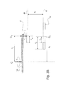
- an anode 20 is shown in the form of a container or vessel having inner conductive surface of copper or stainless steel 22 having an opening 21 at a first end for communicating with a vacuum chamber 2 to which it is directly coupled.
- the outer surface 26 of the container 20 is electrically insulated.
- water cooling pipes 28 are shown substantially around the anode 20 for maintaining the temperature of the anode in operation.
- a gas inlet port 29 is shown for providing a conduit into which sputter gas may enter the anode vessel.
- the size of the opening 21 and the flow of sputter gas can be selected to locally pressurize the anode 20.
- the anode body 20 can be disposed external to or within the vacuum coating chamber 2.
- the opening 21 can be located on a side or end of the anode vessel.
- the relatively small opening 21, significantly smaller than the circumference of the vessel, and the location of the opening 21 out of a line of sight to the target prevent coating material from entering and coating the inner conductive surface of the anode vessel.
- the anode 20 is pressurized with argon gas which promotes the formation of plasma in the coating chamber 2 in the presence of a suitable ignition voltage and maintenance voltage thereafter.
- Positive power supply lead 25 connects the power supply to the inner conductive walls 22 of the anode 20.
- the anode shown in Fig. 5 was designed to function with a low anode voltage and little or no arcing. A low anode voltage of approximately +15 to +60 volts is preferred to reduce process variation.
- the anode 20 is electrically insulated from the grounded chamber walls 32 by an insulating material 33.
- the chamber pressure is below 0.267 Pa (2 mTorr.)
- a higher pressure at the anode is achieved by a constricted opening 21 of the anode 20 and a controlled flow of process gas into the anode 20 via the inlet port 29.
- An optimum opening has an area of about 20cm 2 and is preferably round.
- the anode 20 can be pressurized to more than 0.400 Pa (3mTorr.) This anode 20 can run in nearly continuous operation for extended periods of time.
- the anode vessel 20 can be conveniently located in the chamber walls 32 adjacent the cathode 12 as shown in Fig. 1 also serving as the source of sputter gas.
- An anode vessel 20 can be integrated into the center of the ring cathode, as shown in Fig. 2 , since the anode opening is relatively far away from strong magnetic fields. This improves the symmetry of the system, which improves target utilization.
- Many optical coatings require the deposition of oxides or other compounds.
- Such materials are preferably produced in reactive sputter mode where a metallic target is sputtered and oxygen, nitrogen, or another reactive gas is added to the process.
- the sputtered material and the activated oxygen species arrive simultaneously at the substrate.
- the optimum flow, of oxygen for example, for the optimum oxygen partial pressure needs to be found. If the oxygen flow is too low, the films are not stoichiometric and have high absorption losses. If it is too high, the target surface becomes more oxidized than necessary preventing operation at the highest possible deposition rate.
- the sputter rate for a metallic target can be ten times higher than that of a fully oxidized target.
- the reactive gas flows through a mass flow controller and enters the coating chamber through a simple gas line or a complex manifold.
- the oxidation effectiveness can be increased if the oxygen is activated and directed at the substrates, thus increasing the possible deposition rate.
- the output orifice of an inductively coupled reactive activation source 36 is located in the center of the ring cathode 12.
- a directed oxygen activation or acceleration device 36 shown in Fig. 1 helps the formation of stoichiometric films while minimizing the target oxidation.
- Such a device can be an inductively or capacitively coupled plasma source with or without an extraction or acceleration system.
- the source output can be ionized or otherwise activated oxygen species (e.g. atomic oxygen, ozone). Examples include the JDSU PAS source, a Taurion source from Pro Vac, an APS source from Leybold, or other commercially available ion or activation sources.
- the activated oxygen source 36 is positioned just at the target surface plane 44 in the center of the cathode 12. If the activated reactive source is separated from the cathode, it should be directed such that the cathode 12 is between the oxygen source 36 and the object plane 46 to be outside the line of sight from the sputtered target surface 24, as it is important to prevent massive coating buildup at the oxygen source 36. As shown in Fig.
- the oxygen source 36 can be mounted on a radius r C from C with its opening tilted toward the direction of the target 24 and planet 17.
- the opening should be at a vertical distance greater than or equal to h from the object plane 46. A distance h is preferred. Moving the target surface plane 44 close to the object plane 46 as enabled by the present geometry allows positioning the oxygen activation source 36 closer to the substrates 23 while keeping it free from massive coating buildup. That increases the oxidation effectiveness and allows to coat at higher rates.
- the reactive sputter process is disclosed for oxides. All aspects can similarly be applied to nitrides or other reactive processes.
- the anode vessel 20 has been found to be a suitable structure to provide an activated reactive gas.
- the anode vessel 20 in its typical arrangement contains a plasma.
- the plasma is ignited by the high density of electrons coming from the cathode 12 and returning to the power supply through the anode 20.
- auxiliary activated reactive source located a distance from the cathode 12 (eg. at 20 as shown in Fig. 1 ) can be provided in addition to enable a higher deposition rate.
Landscapes
- Chemical & Material Sciences (AREA)
- Engineering & Computer Science (AREA)
- Physics & Mathematics (AREA)
- Plasma & Fusion (AREA)
- Analytical Chemistry (AREA)
- Chemical Kinetics & Catalysis (AREA)
- Materials Engineering (AREA)
- Mechanical Engineering (AREA)
- Metallurgy (AREA)
- Organic Chemistry (AREA)
- Physical Vapour Deposition (AREA)
Applications Claiming Priority (1)
| Application Number | Priority Date | Filing Date | Title |
|---|---|---|---|
| US32516210P | 2010-04-16 | 2010-04-16 |
Publications (3)
| Publication Number | Publication Date |
|---|---|
| EP2378538A2 true EP2378538A2 (fr) | 2011-10-19 |
| EP2378538A3 EP2378538A3 (fr) | 2014-05-14 |
| EP2378538B1 EP2378538B1 (fr) | 2019-07-24 |
Family
ID=44278672
Family Applications (1)
| Application Number | Title | Priority Date | Filing Date |
|---|---|---|---|
| EP11162661.0A Active EP2378538B1 (fr) | 2010-04-16 | 2011-04-15 | Cathode annulaire pour une utilisation dans un dispositif de pulvérisation magnétron |
Country Status (6)
| Country | Link |
|---|---|
| US (1) | US8480865B2 (fr) |
| EP (1) | EP2378538B1 (fr) |
| JP (1) | JP5619666B2 (fr) |
| KR (2) | KR20110115970A (fr) |
| CN (1) | CN102220561B (fr) |
| TW (4) | TWI648418B (fr) |
Cited By (5)
| Publication number | Priority date | Publication date | Assignee | Title |
|---|---|---|---|---|
| EP2660350A1 (fr) * | 2012-05-04 | 2013-11-06 | JDS Uniphase Corporation | Dépôt par pulvérisation réactive de couches dielectriques |
| EP2509100A3 (fr) * | 2011-04-06 | 2014-05-28 | JDS Uniphase Corporation | Anode intégrée et source de gaz réactif activée pour une utilisation dans un dispositif de pulvérisation de magnétron |
| US9502222B2 (en) | 2010-04-16 | 2016-11-22 | Viavi Solutions Inc. | Integrated anode and activated reactive gas source for use in magnetron sputtering device |
| WO2019246183A1 (fr) * | 2018-06-19 | 2019-12-26 | Applied Materials, Inc. | Système de dépôt à multi-cathode |
| WO2021115758A1 (fr) * | 2019-12-13 | 2021-06-17 | Evatec Ag | Procédé de revêtement par pulvérisation de substrats ou de fabrication de substrats revêtus par pulvérisation et appareil |
Families Citing this family (10)
| Publication number | Priority date | Publication date | Assignee | Title |
|---|---|---|---|---|
| JP5619666B2 (ja) * | 2010-04-16 | 2014-11-05 | ジェイディーエス ユニフェイズ コーポレーションJDS Uniphase Corporation | マグネトロン・スパッタリング・デバイスで使用するためのリング・カソード |
| US20170268095A1 (en) * | 2015-05-04 | 2017-09-21 | University Of Virginia Patent Foundation | Physical vapor deposition on doublet airfoil substrates:controlling the coating thickness |
| US9960199B2 (en) | 2015-12-29 | 2018-05-01 | Viavi Solutions Inc. | Dielectric mirror based multispectral filter array |
| US9923007B2 (en) | 2015-12-29 | 2018-03-20 | Viavi Solutions Inc. | Metal mirror based multispectral filter array |
| DE102018213534A1 (de) | 2018-08-10 | 2020-02-13 | Fraunhofer-Gesellschaft zur Förderung der angewandten Forschung e.V. | Vorrichtung und Verfahren zur Herstellung von Schichten mit verbesserter Uniformität bei Beschichtungsanlagen mit horizontal rotierender Substratführung |
| CN110042346B (zh) * | 2019-05-17 | 2020-02-04 | 济南市半导体元件实验所 | 一种提高蒸铝均匀度的装置、设备及方法 |
| CN110952063B (zh) * | 2019-12-01 | 2022-02-08 | 广东金辉铝板幕墙有限公司 | 一种用于铝板加工防偏转多弧离子复合镀膜机 |
| DE102020201829A1 (de) | 2020-02-13 | 2021-08-19 | Fraunhofer-Gesellschaft zur Förderung der angewandten Forschung eingetragener Verein | Vorrichtung und Verfahren zur Herstellung von Schichten mit verbesserter Uniformität bei Beschichtungsanlagen mit horizontal rotierender Substratführung mit zusätzlichen Plasmaquellen |
| JP7111380B2 (ja) * | 2020-04-01 | 2022-08-02 | 株式会社シンクロン | スパッタ装置及びこれを用いた成膜方法 |
| JP7581953B2 (ja) * | 2021-02-24 | 2024-11-13 | 東京エレクトロン株式会社 | スパッタリング処理を行う装置、及び方法 |
Citations (1)
| Publication number | Priority date | Publication date | Assignee | Title |
|---|---|---|---|---|
| US7424905B2 (en) | 2005-06-16 | 2008-09-16 | Tony Lai | Window blind |
Family Cites Families (23)
| Publication number | Priority date | Publication date | Assignee | Title |
|---|---|---|---|---|
| US4610774A (en) | 1984-11-14 | 1986-09-09 | Hitachi, Ltd. | Target for sputtering |
| US4927515A (en) | 1989-01-09 | 1990-05-22 | The Board Of Trustees Of The Leland Stanford Junior University | Circular magnetron sputtering device |
| JP2975649B2 (ja) * | 1990-07-20 | 1999-11-10 | アネルバ株式会社 | スパッタリング装置 |
| US5366607A (en) | 1991-08-05 | 1994-11-22 | Hmt Technology Corporation | Sputtering target and assembly |
| US5525199A (en) * | 1991-11-13 | 1996-06-11 | Optical Corporation Of America | Low pressure reactive magnetron sputtering apparatus and method |
| JP3378043B2 (ja) * | 1993-03-05 | 2003-02-17 | 同和鉱業株式会社 | スパッタリング装置 |
| JPH08134642A (ja) * | 1994-11-09 | 1996-05-28 | Sony Corp | スパッタリング装置 |
| US5597459A (en) | 1995-02-08 | 1997-01-28 | Nobler Technologies, Inc. | Magnetron cathode sputtering method and apparatus |
| JPH10320852A (ja) * | 1997-05-21 | 1998-12-04 | Nikon Corp | 薄膜形成方法およびそれを用いた光ディスクの製造方法 |
| US6287435B1 (en) | 1998-05-06 | 2001-09-11 | Tokyo Electron Limited | Method and apparatus for ionized physical vapor deposition |
| JP4656744B2 (ja) | 2000-03-09 | 2011-03-23 | キヤノンアネルバ株式会社 | スパッタリング装置 |
| SE519931C2 (sv) * | 2000-06-19 | 2003-04-29 | Chemfilt R & D Ab | Anordning och förfarande för pulsad, starkt joniserad magnetronsputtering |
| JP2002069632A (ja) * | 2000-09-05 | 2002-03-08 | Canon Inc | スパッタ装置およびスパッタ方法 |
| US6638402B2 (en) * | 2001-06-05 | 2003-10-28 | Praxair S.T. Technology, Inc. | Ring-type sputtering target |
| DE10347521A1 (de) | 2002-12-04 | 2004-06-24 | Leybold Optics Gmbh | Verfahren zur Herstellung Multilayerschicht und Vorrichtung zur Durchführung des Verfahrens |
| US20060049041A1 (en) * | 2004-08-20 | 2006-03-09 | Jds Uniphase Corporation | Anode for sputter coating |
| US7879209B2 (en) * | 2004-08-20 | 2011-02-01 | Jds Uniphase Corporation | Cathode for sputter coating |
| US8500973B2 (en) * | 2004-08-20 | 2013-08-06 | Jds Uniphase Corporation | Anode for sputter coating |
| DK1630260T3 (da) * | 2004-08-20 | 2011-10-31 | Jds Uniphase Inc | Magnetisk holdemekanisme til et dampudfældningssystem |
| JP5194427B2 (ja) * | 2006-10-27 | 2013-05-08 | 株式会社ブリヂストン | 光触媒酸化タングステン薄膜 |
| TW200839021A (en) * | 2007-03-20 | 2008-10-01 | Japan Science & Tech Agency | Spattering apparatus and spattering method |
| TWI359872B (en) * | 2007-11-15 | 2012-03-11 | Wintek Corp | Magnetron sputter cathode mechanism |
| JP5619666B2 (ja) * | 2010-04-16 | 2014-11-05 | ジェイディーエス ユニフェイズ コーポレーションJDS Uniphase Corporation | マグネトロン・スパッタリング・デバイスで使用するためのリング・カソード |
-
2011
- 2011-04-12 JP JP2011088373A patent/JP5619666B2/ja active Active
- 2011-04-14 US US13/087,301 patent/US8480865B2/en active Active
- 2011-04-14 KR KR1020110034655A patent/KR20110115970A/ko not_active Ceased
- 2011-04-15 TW TW105116905A patent/TWI648418B/zh active
- 2011-04-15 TW TW108143550A patent/TWI749412B/zh active
- 2011-04-15 EP EP11162661.0A patent/EP2378538B1/fr active Active
- 2011-04-15 TW TW107106301A patent/TWI682049B/zh active
- 2011-04-15 TW TW100113269A patent/TWI548767B/zh active
- 2011-04-18 CN CN201110096949.2A patent/CN102220561B/zh active Active
-
2018
- 2018-01-02 KR KR1020180000395A patent/KR101920907B1/ko active Active
Patent Citations (1)
| Publication number | Priority date | Publication date | Assignee | Title |
|---|---|---|---|---|
| US7424905B2 (en) | 2005-06-16 | 2008-09-16 | Tony Lai | Window blind |
Cited By (9)
| Publication number | Priority date | Publication date | Assignee | Title |
|---|---|---|---|---|
| US9502222B2 (en) | 2010-04-16 | 2016-11-22 | Viavi Solutions Inc. | Integrated anode and activated reactive gas source for use in magnetron sputtering device |
| EP2509100A3 (fr) * | 2011-04-06 | 2014-05-28 | JDS Uniphase Corporation | Anode intégrée et source de gaz réactif activée pour une utilisation dans un dispositif de pulvérisation de magnétron |
| EP2660350A1 (fr) * | 2012-05-04 | 2013-11-06 | JDS Uniphase Corporation | Dépôt par pulvérisation réactive de couches dielectriques |
| US9988705B2 (en) | 2012-05-04 | 2018-06-05 | Viavi Solutions Inc. | Reactive sputter deposition of silicon films |
| US10920310B2 (en) | 2012-05-04 | 2021-02-16 | Viavi Solutions Inc. | Reactive sputter deposition of dielectric films |
| US11584982B2 (en) | 2012-05-04 | 2023-02-21 | Viavi Solutions Inc. | Reactive sputter deposition of dielectric films |
| US12545987B2 (en) | 2012-05-04 | 2026-02-10 | Viavi Solutions Inc. | Reactive sputter deposition of dielectric films |
| WO2019246183A1 (fr) * | 2018-06-19 | 2019-12-26 | Applied Materials, Inc. | Système de dépôt à multi-cathode |
| WO2021115758A1 (fr) * | 2019-12-13 | 2021-06-17 | Evatec Ag | Procédé de revêtement par pulvérisation de substrats ou de fabrication de substrats revêtus par pulvérisation et appareil |
Also Published As
| Publication number | Publication date |
|---|---|
| US20110253529A1 (en) | 2011-10-20 |
| KR20110115970A (ko) | 2011-10-24 |
| TW201833359A (zh) | 2018-09-16 |
| US8480865B2 (en) | 2013-07-09 |
| HK1162619A1 (en) | 2012-08-31 |
| TW201700760A (zh) | 2017-01-01 |
| JP5619666B2 (ja) | 2014-11-05 |
| KR20180004845A (ko) | 2018-01-12 |
| EP2378538B1 (fr) | 2019-07-24 |
| TWI682049B (zh) | 2020-01-11 |
| JP2011225992A (ja) | 2011-11-10 |
| TW202026446A (zh) | 2020-07-16 |
| CN102220561B (zh) | 2015-04-22 |
| CN102220561A (zh) | 2011-10-19 |
| KR101920907B1 (ko) | 2018-11-21 |
| TWI648418B (zh) | 2019-01-21 |
| TWI749412B (zh) | 2021-12-11 |
| TW201142064A (en) | 2011-12-01 |
| EP2378538A3 (fr) | 2014-05-14 |
| TWI548767B (zh) | 2016-09-11 |
Similar Documents
| Publication | Publication Date | Title |
|---|---|---|
| EP2378538B1 (fr) | Cathode annulaire pour une utilisation dans un dispositif de pulvérisation magnétron | |
| US6562200B2 (en) | Thin-film formation system and thin-film formation process | |
| US8163144B2 (en) | Magnetron sputtering device | |
| KR102616067B1 (ko) | Pvd 스퍼터링 증착 챔버의 경사형 마그네트론 | |
| US20090194412A1 (en) | Multi-cathode ionized physical vapor deposition system | |
| KR20070008369A (ko) | 큰 영역 기판의 마그네트론 스퍼터링 시스템 | |
| EP2509100B1 (fr) | Anode et source de gaz réactif activé intégrées pour une utilisation dans un dispositif de pulvérisation magnétron | |
| EP3449496B1 (fr) | Kit de traitement pour une chambre de traitement au plasma | |
| US9502222B2 (en) | Integrated anode and activated reactive gas source for use in magnetron sputtering device | |
| HK1162619B (en) | Ring cathode for use in a magnetron sputtering device |
Legal Events
| Date | Code | Title | Description |
|---|---|---|---|
| AK | Designated contracting states |
Kind code of ref document: A2 Designated state(s): AL AT BE BG CH CY CZ DE DK EE ES FI FR GB GR HR HU IE IS IT LI LT LU LV MC MK MT NL NO PL PT RO RS SE SI SK SM TR |
|
| AX | Request for extension of the european patent |
Extension state: BA ME |
|
| PUAI | Public reference made under article 153(3) epc to a published international application that has entered the european phase |
Free format text: ORIGINAL CODE: 0009012 |
|
| PUAL | Search report despatched |
Free format text: ORIGINAL CODE: 0009013 |
|
| AK | Designated contracting states |
Kind code of ref document: A3 Designated state(s): AL AT BE BG CH CY CZ DE DK EE ES FI FR GB GR HR HU IE IS IT LI LT LU LV MC MK MT NL NO PL PT RO RS SE SI SK SM TR |
|
| AX | Request for extension of the european patent |
Extension state: BA ME |
|
| RIC1 | Information provided on ipc code assigned before grant |
Ipc: H01J 37/34 20060101AFI20140407BHEP Ipc: C23C 14/50 20060101ALI20140407BHEP |
|
| 17P | Request for examination filed |
Effective date: 20141111 |
|
| RBV | Designated contracting states (corrected) |
Designated state(s): AL AT BE BG CH CY CZ DE DK EE ES FI FR GB GR HR HU IE IS IT LI LT LU LV MC MK MT NL NO PL PT RO RS SE SI SK SM TR |
|
| RAP1 | Party data changed (applicant data changed or rights of an application transferred) |
Owner name: VIAVI SOLUTIONS INC. |
|
| RAP1 | Party data changed (applicant data changed or rights of an application transferred) |
Owner name: VIAVI SOLUTIONS INC. |
|
| GRAP | Despatch of communication of intention to grant a patent |
Free format text: ORIGINAL CODE: EPIDOSNIGR1 |
|
| STAA | Information on the status of an ep patent application or granted ep patent |
Free format text: STATUS: GRANT OF PATENT IS INTENDED |
|
| RIC1 | Information provided on ipc code assigned before grant |
Ipc: H01J 37/34 20060101AFI20190207BHEP Ipc: C23C 14/50 20060101ALI20190207BHEP Ipc: C23C 14/00 20060101ALI20190207BHEP |
|
| INTG | Intention to grant announced |
Effective date: 20190226 |
|
| GRAS | Grant fee paid |
Free format text: ORIGINAL CODE: EPIDOSNIGR3 |
|
| GRAA | (expected) grant |
Free format text: ORIGINAL CODE: 0009210 |
|
| STAA | Information on the status of an ep patent application or granted ep patent |
Free format text: STATUS: THE PATENT HAS BEEN GRANTED |
|
| AK | Designated contracting states |
Kind code of ref document: B1 Designated state(s): AL AT BE BG CH CY CZ DE DK EE ES FI FR GB GR HR HU IE IS IT LI LT LU LV MC MK MT NL NO PL PT RO RS SE SI SK SM TR |
|
| REG | Reference to a national code |
Ref country code: GB Ref legal event code: FG4D |
|
| REG | Reference to a national code |
Ref country code: CH Ref legal event code: EP |
|
| REG | Reference to a national code |
Ref country code: DE Ref legal event code: R096 Ref document number: 602011060611 Country of ref document: DE |
|
| REG | Reference to a national code |
Ref country code: CH Ref legal event code: NV Representative=s name: MURGITROYD AND COMPANY, CH Ref country code: AT Ref legal event code: REF Ref document number: 1159205 Country of ref document: AT Kind code of ref document: T Effective date: 20190815 |
|
| REG | Reference to a national code |
Ref country code: IE Ref legal event code: FG4D |
|
| REG | Reference to a national code |
Ref country code: SE Ref legal event code: TRGR |
|
| REG | Reference to a national code |
Ref country code: NL Ref legal event code: MP Effective date: 20190724 |
|
| REG | Reference to a national code |
Ref country code: LT Ref legal event code: MG4D |
|
| REG | Reference to a national code |
Ref country code: AT Ref legal event code: MK05 Ref document number: 1159205 Country of ref document: AT Kind code of ref document: T Effective date: 20190724 |
|
| PG25 | Lapsed in a contracting state [announced via postgrant information from national office to epo] |
Ref country code: BG Free format text: LAPSE BECAUSE OF FAILURE TO SUBMIT A TRANSLATION OF THE DESCRIPTION OR TO PAY THE FEE WITHIN THE PRESCRIBED TIME-LIMIT Effective date: 20191024 Ref country code: NO Free format text: LAPSE BECAUSE OF FAILURE TO SUBMIT A TRANSLATION OF THE DESCRIPTION OR TO PAY THE FEE WITHIN THE PRESCRIBED TIME-LIMIT Effective date: 20191024 Ref country code: AT Free format text: LAPSE BECAUSE OF FAILURE TO SUBMIT A TRANSLATION OF THE DESCRIPTION OR TO PAY THE FEE WITHIN THE PRESCRIBED TIME-LIMIT Effective date: 20190724 Ref country code: HR Free format text: LAPSE BECAUSE OF FAILURE TO SUBMIT A TRANSLATION OF THE DESCRIPTION OR TO PAY THE FEE WITHIN THE PRESCRIBED TIME-LIMIT Effective date: 20190724 Ref country code: FI Free format text: LAPSE BECAUSE OF FAILURE TO SUBMIT A TRANSLATION OF THE DESCRIPTION OR TO PAY THE FEE WITHIN THE PRESCRIBED TIME-LIMIT Effective date: 20190724 Ref country code: PT Free format text: LAPSE BECAUSE OF FAILURE TO SUBMIT A TRANSLATION OF THE DESCRIPTION OR TO PAY THE FEE WITHIN THE PRESCRIBED TIME-LIMIT Effective date: 20191125 Ref country code: NL Free format text: LAPSE BECAUSE OF FAILURE TO SUBMIT A TRANSLATION OF THE DESCRIPTION OR TO PAY THE FEE WITHIN THE PRESCRIBED TIME-LIMIT Effective date: 20190724 Ref country code: LT Free format text: LAPSE BECAUSE OF FAILURE TO SUBMIT A TRANSLATION OF THE DESCRIPTION OR TO PAY THE FEE WITHIN THE PRESCRIBED TIME-LIMIT Effective date: 20190724 |
|
| PG25 | Lapsed in a contracting state [announced via postgrant information from national office to epo] |
Ref country code: GR Free format text: LAPSE BECAUSE OF FAILURE TO SUBMIT A TRANSLATION OF THE DESCRIPTION OR TO PAY THE FEE WITHIN THE PRESCRIBED TIME-LIMIT Effective date: 20191025 Ref country code: ES Free format text: LAPSE BECAUSE OF FAILURE TO SUBMIT A TRANSLATION OF THE DESCRIPTION OR TO PAY THE FEE WITHIN THE PRESCRIBED TIME-LIMIT Effective date: 20190724 Ref country code: RS Free format text: LAPSE BECAUSE OF FAILURE TO SUBMIT A TRANSLATION OF THE DESCRIPTION OR TO PAY THE FEE WITHIN THE PRESCRIBED TIME-LIMIT Effective date: 20190724 Ref country code: AL Free format text: LAPSE BECAUSE OF FAILURE TO SUBMIT A TRANSLATION OF THE DESCRIPTION OR TO PAY THE FEE WITHIN THE PRESCRIBED TIME-LIMIT Effective date: 20190724 Ref country code: LV Free format text: LAPSE BECAUSE OF FAILURE TO SUBMIT A TRANSLATION OF THE DESCRIPTION OR TO PAY THE FEE WITHIN THE PRESCRIBED TIME-LIMIT Effective date: 20190724 Ref country code: IS Free format text: LAPSE BECAUSE OF FAILURE TO SUBMIT A TRANSLATION OF THE DESCRIPTION OR TO PAY THE FEE WITHIN THE PRESCRIBED TIME-LIMIT Effective date: 20191124 |
|
| PG25 | Lapsed in a contracting state [announced via postgrant information from national office to epo] |
Ref country code: TR Free format text: LAPSE BECAUSE OF FAILURE TO SUBMIT A TRANSLATION OF THE DESCRIPTION OR TO PAY THE FEE WITHIN THE PRESCRIBED TIME-LIMIT Effective date: 20190724 |
|
| PG25 | Lapsed in a contracting state [announced via postgrant information from national office to epo] |
Ref country code: PL Free format text: LAPSE BECAUSE OF FAILURE TO SUBMIT A TRANSLATION OF THE DESCRIPTION OR TO PAY THE FEE WITHIN THE PRESCRIBED TIME-LIMIT Effective date: 20190724 Ref country code: RO Free format text: LAPSE BECAUSE OF FAILURE TO SUBMIT A TRANSLATION OF THE DESCRIPTION OR TO PAY THE FEE WITHIN THE PRESCRIBED TIME-LIMIT Effective date: 20190724 Ref country code: DK Free format text: LAPSE BECAUSE OF FAILURE TO SUBMIT A TRANSLATION OF THE DESCRIPTION OR TO PAY THE FEE WITHIN THE PRESCRIBED TIME-LIMIT Effective date: 20190724 Ref country code: EE Free format text: LAPSE BECAUSE OF FAILURE TO SUBMIT A TRANSLATION OF THE DESCRIPTION OR TO PAY THE FEE WITHIN THE PRESCRIBED TIME-LIMIT Effective date: 20190724 Ref country code: IT Free format text: LAPSE BECAUSE OF FAILURE TO SUBMIT A TRANSLATION OF THE DESCRIPTION OR TO PAY THE FEE WITHIN THE PRESCRIBED TIME-LIMIT Effective date: 20190724 |
|
| PG25 | Lapsed in a contracting state [announced via postgrant information from national office to epo] |
Ref country code: IS Free format text: LAPSE BECAUSE OF FAILURE TO SUBMIT A TRANSLATION OF THE DESCRIPTION OR TO PAY THE FEE WITHIN THE PRESCRIBED TIME-LIMIT Effective date: 20200224 Ref country code: SM Free format text: LAPSE BECAUSE OF FAILURE TO SUBMIT A TRANSLATION OF THE DESCRIPTION OR TO PAY THE FEE WITHIN THE PRESCRIBED TIME-LIMIT Effective date: 20190724 Ref country code: SK Free format text: LAPSE BECAUSE OF FAILURE TO SUBMIT A TRANSLATION OF THE DESCRIPTION OR TO PAY THE FEE WITHIN THE PRESCRIBED TIME-LIMIT Effective date: 20190724 Ref country code: CZ Free format text: LAPSE BECAUSE OF FAILURE TO SUBMIT A TRANSLATION OF THE DESCRIPTION OR TO PAY THE FEE WITHIN THE PRESCRIBED TIME-LIMIT Effective date: 20190724 |
|
| REG | Reference to a national code |
Ref country code: DE Ref legal event code: R097 Ref document number: 602011060611 Country of ref document: DE |
|
| PLBE | No opposition filed within time limit |
Free format text: ORIGINAL CODE: 0009261 |
|
| STAA | Information on the status of an ep patent application or granted ep patent |
Free format text: STATUS: NO OPPOSITION FILED WITHIN TIME LIMIT |
|
| PG2D | Information on lapse in contracting state deleted |
Ref country code: IS |
|
| 26N | No opposition filed |
Effective date: 20200603 |
|
| PG25 | Lapsed in a contracting state [announced via postgrant information from national office to epo] |
Ref country code: SI Free format text: LAPSE BECAUSE OF FAILURE TO SUBMIT A TRANSLATION OF THE DESCRIPTION OR TO PAY THE FEE WITHIN THE PRESCRIBED TIME-LIMIT Effective date: 20190724 |
|
| PG25 | Lapsed in a contracting state [announced via postgrant information from national office to epo] |
Ref country code: MC Free format text: LAPSE BECAUSE OF FAILURE TO SUBMIT A TRANSLATION OF THE DESCRIPTION OR TO PAY THE FEE WITHIN THE PRESCRIBED TIME-LIMIT Effective date: 20190724 |
|
| PG25 | Lapsed in a contracting state [announced via postgrant information from national office to epo] |
Ref country code: LU Free format text: LAPSE BECAUSE OF NON-PAYMENT OF DUE FEES Effective date: 20200415 |
|
| REG | Reference to a national code |
Ref country code: BE Ref legal event code: MM Effective date: 20200430 |
|
| PG25 | Lapsed in a contracting state [announced via postgrant information from national office to epo] |
Ref country code: BE Free format text: LAPSE BECAUSE OF NON-PAYMENT OF DUE FEES Effective date: 20200430 |
|
| PG25 | Lapsed in a contracting state [announced via postgrant information from national office to epo] |
Ref country code: IE Free format text: LAPSE BECAUSE OF NON-PAYMENT OF DUE FEES Effective date: 20200415 |
|
| PG25 | Lapsed in a contracting state [announced via postgrant information from national office to epo] |
Ref country code: MT Free format text: LAPSE BECAUSE OF FAILURE TO SUBMIT A TRANSLATION OF THE DESCRIPTION OR TO PAY THE FEE WITHIN THE PRESCRIBED TIME-LIMIT Effective date: 20190724 Ref country code: CY Free format text: LAPSE BECAUSE OF FAILURE TO SUBMIT A TRANSLATION OF THE DESCRIPTION OR TO PAY THE FEE WITHIN THE PRESCRIBED TIME-LIMIT Effective date: 20190724 |
|
| PG25 | Lapsed in a contracting state [announced via postgrant information from national office to epo] |
Ref country code: MK Free format text: LAPSE BECAUSE OF FAILURE TO SUBMIT A TRANSLATION OF THE DESCRIPTION OR TO PAY THE FEE WITHIN THE PRESCRIBED TIME-LIMIT Effective date: 20190724 |
|
| P01 | Opt-out of the competence of the unified patent court (upc) registered |
Effective date: 20230530 |
|
| PGFP | Annual fee paid to national office [announced via postgrant information from national office to epo] |
Ref country code: DE Payment date: 20250430 Year of fee payment: 15 |
|
| PGFP | Annual fee paid to national office [announced via postgrant information from national office to epo] |
Ref country code: FR Payment date: 20250429 Year of fee payment: 15 |
|
| PGFP | Annual fee paid to national office [announced via postgrant information from national office to epo] |
Ref country code: CH Payment date: 20250501 Year of fee payment: 15 |
|
| PGFP | Annual fee paid to national office [announced via postgrant information from national office to epo] |
Ref country code: SE Payment date: 20250429 Year of fee payment: 15 |
|
| PGFP | Annual fee paid to national office [announced via postgrant information from national office to epo] |
Ref country code: GB Payment date: 20260331 Year of fee payment: 16 |