EP2378548A1 - Procédés de traitement et d'inspection de substrats de semi-conducteur - Google Patents
Procédés de traitement et d'inspection de substrats de semi-conducteur Download PDFInfo
- Publication number
- EP2378548A1 EP2378548A1 EP20100004141 EP10004141A EP2378548A1 EP 2378548 A1 EP2378548 A1 EP 2378548A1 EP 20100004141 EP20100004141 EP 20100004141 EP 10004141 A EP10004141 A EP 10004141A EP 2378548 A1 EP2378548 A1 EP 2378548A1
- Authority
- EP
- European Patent Office
- Prior art keywords
- substrate
- measuring light
- back surface
- wafer
- thinning process
- Prior art date
- Legal status (The legal status is an assumption and is not a legal conclusion. Google has not performed a legal analysis and makes no representation as to the accuracy of the status listed.)
- Withdrawn
Links
Images

Classifications
-
- H—ELECTRICITY
- H10—SEMICONDUCTOR DEVICES; ELECTRIC SOLID-STATE DEVICES NOT OTHERWISE PROVIDED FOR
- H10P—GENERIC PROCESSES OR APPARATUS FOR THE MANUFACTURE OR TREATMENT OF DEVICES COVERED BY CLASS H10
- H10P74/00—Testing or measuring during manufacture or treatment of wafers, substrates or devices
- H10P74/20—Testing or measuring during manufacture or treatment of wafers, substrates or devices characterised by the properties tested or measured, e.g. structural or electrical properties
- H10P74/203—Structural properties, e.g. testing or measuring thicknesses, line widths, warpage, bond strengths or physical defects
-
- G—PHYSICS
- G01—MEASURING; TESTING
- G01N—INVESTIGATING OR ANALYSING MATERIALS BY DETERMINING THEIR CHEMICAL OR PHYSICAL PROPERTIES
- G01N21/00—Investigating or analysing materials by the use of optical means, i.e. using sub-millimetre waves, infrared, visible or ultraviolet light
- G01N21/84—Systems specially adapted for particular applications
- G01N21/88—Investigating the presence of flaws or contamination
- G01N21/95—Investigating the presence of flaws or contamination characterised by the material or shape of the object to be examined
- G01N21/9501—Semiconductor wafers
-
- H—ELECTRICITY
- H10—SEMICONDUCTOR DEVICES; ELECTRIC SOLID-STATE DEVICES NOT OTHERWISE PROVIDED FOR
- H10P—GENERIC PROCESSES OR APPARATUS FOR THE MANUFACTURE OR TREATMENT OF DEVICES COVERED BY CLASS H10
- H10P74/00—Testing or measuring during manufacture or treatment of wafers, substrates or devices
- H10P74/23—Testing or measuring during manufacture or treatment of wafers, substrates or devices characterised by multiple measurements, corrections, marking or sorting processes
- H10P74/238—Testing or measuring during manufacture or treatment of wafers, substrates or devices characterised by multiple measurements, corrections, marking or sorting processes comprising acting in response to an ongoing measurement without interruption of processing, e.g. endpoint detection or in-situ thickness measurement
-
- H—ELECTRICITY
- H10—SEMICONDUCTOR DEVICES; ELECTRIC SOLID-STATE DEVICES NOT OTHERWISE PROVIDED FOR
- H10W—GENERIC PACKAGES, INTERCONNECTIONS, CONNECTORS OR OTHER CONSTRUCTIONAL DETAILS OF DEVICES COVERED BY CLASS H10
- H10W20/00—Interconnections in chips, wafers or substrates
- H10W20/01—Manufacture or treatment
- H10W20/021—Manufacture or treatment of interconnections within wafers or substrates
- H10W20/023—Manufacture or treatment of interconnections within wafers or substrates the interconnections being through-semiconductor vias
-
- H—ELECTRICITY
- H10—SEMICONDUCTOR DEVICES; ELECTRIC SOLID-STATE DEVICES NOT OTHERWISE PROVIDED FOR
- H10W—GENERIC PACKAGES, INTERCONNECTIONS, CONNECTORS OR OTHER CONSTRUCTIONAL DETAILS OF DEVICES COVERED BY CLASS H10
- H10W20/00—Interconnections in chips, wafers or substrates
- H10W20/01—Manufacture or treatment
- H10W20/021—Manufacture or treatment of interconnections within wafers or substrates
- H10W20/023—Manufacture or treatment of interconnections within wafers or substrates the interconnections being through-semiconductor vias
- H10W20/0245—Manufacture or treatment of interconnections within wafers or substrates the interconnections being through-semiconductor vias comprising use of blind vias during the manufacture
-
- G—PHYSICS
- G01—MEASURING; TESTING
- G01N—INVESTIGATING OR ANALYSING MATERIALS BY DETERMINING THEIR CHEMICAL OR PHYSICAL PROPERTIES
- G01N21/00—Investigating or analysing materials by the use of optical means, i.e. using sub-millimetre waves, infrared, visible or ultraviolet light
- G01N21/84—Systems specially adapted for particular applications
- G01N21/88—Investigating the presence of flaws or contamination
- G01N21/95—Investigating the presence of flaws or contamination characterised by the material or shape of the object to be examined
- G01N21/9501—Semiconductor wafers
- G01N21/9505—Wafer internal defects, e.g. microcracks
Definitions
- the invention relates to methods of inspecting semiconductor substrates and to methods of processing semiconductor substrates.
- the invention also relates to methods of manufacturing semiconductor devices and to devices manufactured using such methods.
- a semiconductor wafer substrate generally includes a front side having integrated circuits formed thereon, and a bulk of semiconductor material providing the back side of substrate. Prior to bonding and packaging of individual integrated circuit chips or bonding to other semiconductor substrates, the wafer substrate is typically thinned to remove unwanted semiconductor material or to expose through wafer vias embedded in the substrate to provide electrical contact from the back side to the integrated circuits formed on the front side.
- the present invention has been accomplished taking the above problems into consideration.
- the processing of semiconductor substrates includes optical methods to determine a distance between a piece of metal embedded in a semiconductor substrate and a back surface of the substrate.
- optical methods are used to detect pieces of metal embedded in the substrate and not exposed at the back surface of the substrate and to control a wafer thinning process based on such detection.
- information gained by the optical methods from one wafer can be used to control a subsequent thinning process applied to the same wafer or to control a thinning process applied to a next wafer.
- other information such as information relating to grinding marks detected on the back surface, can be used to control a subsequent grinding process applied to a next wafer.
- the optical methods include directing measuring light towards the back surface of the substrate and detecting a portion of the measuring light received back from the substrate.
- the direction of measuring light towards the back surface and the detection of the portion of measuring light received back from the substrate uses a dark field configuration.
- a minimum angle between a direction of a portion of the measuring light reflected off the back surface and a direction of the portion of the measuring light received back from the substrate is greater than 10°, greater than 20° or greater than 30°.
- the inventors have found that a dark field configuration which is conventionally used to detect defects, such as particles or scratches, on a substrate surface can be successfully applied to detect features embedded in the bulk of the substrate. Such features may comprise pieces of metal embedded in a substrate made of semiconductor material.
- the optical methods comprise imaging of a portion of the substrate onto a position sensitive detector.
- a lateral extension of the feature embedded in the bulk of the substrate is at least 2 times smaller or at least 5 times smaller than a lateral resolution of the imaging of the portion of the substrate onto the position sensitive detector.
- a lateral extension of a region of a substrate imaged onto one single pixel of a position sensitive detector is at least ten times greater or at least 20 times greater than a lateral extension of the features embedded in the substrate.
- the optical methods include directing of a measuring light beam onto the substrate such that a lateral extension of the beam of measuring light on the back surface is at least 2 times greater, at least 5 times, at least 10 times, or at least 100 times greater than a lateral extension of the feature embedded in the substrate.
- the beam of measuring light can be scanned across the substrate to generate an image of the substrate and to perform the optical methods at plural locations of the substrate.
- measuring light used in the optical methods has wavelengths selected such that a penetration depth of the measuring light into the substrate material is greater than 0.2 times, 0.5 times or 1.5 times a distance between features embedded in the substrate and the back surface of the substrate.
- the substrate material is silicon, and the wavelengths of the measuring light are greater than 500 nm, 550 nm, 600 nm or 650 nm.
- wavelengths of measuring light used in the optical methods are selected such that a penetration depth of the measuring light into the substrate is less than 2.0 times, 1.0 times or 0.5 times a distance between the back surface of the substrate and a front surface of the substrate opposite to the back surface.
- the substrate material is silicon, and the wavelengths of the measuring light are smaller than 900 nm, 850 nm, 800 nm or 750 nm.
- the pieces of metal embedded in the substrate material are through wafer vias, i.e. conductive connectors extending from a front side of the substrate into the substrate.
- a thinning process is applied to a back side of the substrate to remove substrate material.
- the thinning process comprises grinding and/or etching.
- the thinning process may be controlled based on information gained in one of the optical methods disclosed in this application.
- a method of manufacturing a semiconductor device comprises forming semiconductor structures and through wafer vias on a front side of a first semiconductor substrate, bonding the first substrate with its front side to a carrier, applying at least one thinning process to the first substrate by removing substrate material at a back side of the substrate such that the through wafer vias are exposed at the back side, and bonding at least one second substrate to the first substrate, wherein the at least one thinning process is controlled based on information gained from one of the optical methods illustrated above.
- the embodiments illustrated below generally relate to manufacture of semiconductor devices and to thinning of wafers and in particular to thinning of such wafers including through wafer vias which are to be exposed at a back side of the wafer by applying a thinning process to the back side of the wafer.
- Background information relating to thinning of wafers and to wafers including through wafer vias can be obtained from US 7,214,615 B2 , US 6,916,725 B2 , US 2010/0038800 A1 , US 2010/0032764 A1 , US 2005/0158889 A1 and US 2010/0041226 A1 , wherein the full disclosure of these documents is incorporated herein by reference.
- the illustrated embodiments relate to thinning of wafers and involve optical methods used for determining a residual thickness between tip ends of through wafer vias and a back surface of a wafer and for obtaining information which can be used for controlling a thinning process. These optical methods are, however, not limited to those applications. The optical methods can be also applied to other substrates in which features are embedded in the substrate such that they are located below a surface of the substrate.
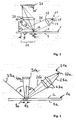
- Figure 1 is a schematic illustration of a cross section of a semiconductor wafer in a manufacturing process for semiconductor devices.
- the wafer 1 has a front surface 6 at a front side 3 and a back surface 5 at a back side 4.
- a plurality of semiconductor devices 7, such as field effect transistors, are formed at the front side 3 of the wafer 1 by applying a plurality of lithographic steps and other manufacturing steps to the front side 3 of the wafer 1.
- Through wafer vias 9 extend from the front side 3 into the substrate material of the wafer 1.
- the through wafer vias 9 can be formed by conventional methods, such as etching trenches into the substrate, depositing insulating material on trench walls and filling the trenches with a conductive material, such as copper.
- the through wafer vias have a high aspect ratio and extend into the substrate of the wafer such that tip ends 11 of the through wafer vias 9 are located at a residual distance d 1 from back surface 5 of the wafer 1.
- Exemplary values of the residual distance d 1 after manufacture of the through wafer vias 9 include 630 ⁇ m and 730 ⁇ m, depending on a thickness of the wafer 1.
- One or more wafer thinning processes will be applied to the wafer 1 schematically illustrated in Figure 1 to expose the vias 9 at the back surface of the wafer.
- the thinning process includes removal of substrate material from the back surface 5 of the wafer 1.
- a broken line 5' in Figure 1 illustrates a position of the back surface of the wafer after thinning such that the vias 9 are exposed and project a distance d 2 from the surface.
- Exemplary values of the distance d 2 are 1 ⁇ m and 2 ⁇ m, for example. It is apparent that the thinning process has to be performed with a high accuracy to maintain the achieved distances d 2 within an acceptable range for all the vias 9 distributed across the substrate 1. Therefore, it is desirable to control the one or more thinning processes based on measurements.
- a conventional optical measurement to control wafer thinning is known from US 2005/0158889 A1 and measures a distance between the back surface 5 and the front surface 4 of the wafer.
- This conventional optical measurement method uses infrared light having a penetration depth in the wafer material which is greater than the distance between the front and back surfaces. Problems in the conventional method may occur if it is not possible to precisely detect the front surface of the wafer due to a presence of a carrier substrate onto which the wafer is attached with its front side 3, and if a depth by which the vias extend into the substrate is not exactly known or not uniform across the wafer.
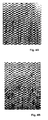
- FIG 2 is a schematic illustration of an optical configuration which can be used to perform an optical method for determining the residual thickness d 1 of the wafer 1 schematically illustrated in Figure 1 .
- the optical configuration includes a light source 21 to generate measuring light 23 from which a beam 25 of measuring light is shaped by optics 27.
- the optics 27 may include one or more lenses and one or more mirrors.
- the beam 25 is directed onto a portion 29 of the back surface 5 of the wafer 1 under an angle ⁇ relative to a surface normal which is greater than, for example, 10°, 20° or 30°.
- the portion 29 of the back surface 5 of the wafer is imaged onto a position sensitive detector 31 using imaging optics 33.
- the imaging optics 33 may include one or more lenses and one or more mirrors.
- the position sensitive detector 31 comprises an array of pixels 35.
- the position sensitive detector 31 may have a high number of pixels, such as 10,000 or more pixels, wherein a number of only six pixels 35 is shown in Figure 5 for illustrative purposes. Due to the imaging with imaging optics 33, there is a one-to-one correspondence between regions on the wafer 1 and individual pixels onto which each region is imaged.
- Reference numeral 37 indicates an exemplary region on the substrate 1 which is imaged onto the left pixel 35 of detector 31 shown in Figure 2 .
- a lateral extension d 3 of the region 37 imaged onto the one pixel 35 is, for example, 100 ⁇ m. This lateral extension is greater than the lateral extension of the vias 9 embedded in the substrate.
- An exemplary value of the lateral extension of a via 9 is 2 ⁇ m to 20 ⁇ m.
- the optical configuration illustrated in Figure 2 is a dark field configuration as illustrated by an angle P shown in Figure 2 .
- the angle P is a minimum angle between rays 39 of measuring light 25 specularly reflected at the back surface 5 of the wafer and rays 41 of the portion of the measuring light scattered at the wafer 1 and received by the detector 31.
- This minimum angle P is greater than 10°, 20° or 30°, for example.
- Wavelengths of the light of the measuring beam 25 are selected to fulfil certain requirements illustrated below in more detail.
- transmissive filters allowing only certain wavelengths to traverse or reflective filters reflecting only certain wavelengths can be disposed in the beam path of the measuring light beam 25.
- the measuring light beam 25 includes a generally broad spectrum of wavelengths and wherein a wavelength selection is performed in the imaging beam path between the substrate 1 and the detector 31 by providing suitable transmissive or reflective filters.
- the light source 21 can be configured such that it generates substantially only light from a desired wavelength range.
- the portion 29 which is imaged onto the detector 31 may have a lateral extension such that plural through wafer vias 9 are located within the region 29.
- the number of vias located within the region 29 may exceed 100 vias or many thousand vias.
- the lateral extension of the region 29 can be greater than a lateral extension of dice formed from the wafer 1 later by dicing.
- the lateral extension of the region 29 can be selected such that it includes more than one, more than two, more than five or even more dice.
- the region 29 imaged onto the detector 31 may include the full wafer 1 such that the lateral extension of the region 29 can be greater than 200 mm or greater than 300 mm depending on the diameter of the wafer 1.
- An example of an optical configuration which can be used in optical methods illustrated in the present disclosure is illustrated in WO 2009/121628 A2 , the full disclosure of which is incorporated herein by reference.
- FIG. 3 An alternative optical configuration which can be used in the optical methods illustrated in this disclosure is schematically shown in Figure 3 .
- This setup includes a light source 21a generating measuring light 23a which is shaped to a focussed beam 25a of measuring light by optics 27a which may comprise one or more lenses and one or more mirrors.
- the focused beam 25a of measuring light is directed onto a back surface 5a of a wafer 1a such that a lateral extension d 3 of the beam 25 at the back surface 5a is greater than a lateral extension of through wafer vias 9a embedded in the wafer substrate.
- the lateral extension d 3 can be 2 times greater, 5 times greater, 10 times greater or even 100 times greater than the lateral extension of the through wafer vias 9a.
- the beam of measuring light 25a is directed onto the substrate 1a under an angle ⁇ relative to a surface normal of the wafer 1a.
- a detector 31a is positioned such that a minimum angle ⁇ of rays 39a of measuring light 25a specularly reflected at the back surface 6a of the wafer and rays 41a of the measuring light received by the detector 31a is greater than 10°, 20° or 30°, for example.
- the detector 31a may include one single light sensitive element or a number of light sensitive element. While it is possible that the detector 31a is a position sensitive detector, this is not necessary in the illustrated configuration.
- An image of the wafer 1a can be obtained by scanning the beam 25a across the back surface 5a of the wafer and recording light intensities detected with the detector 31a in dependence of a position to which the beam 25a is directed. For example, the wafer 1a can be rotated and/or otherwise displaced relative to the beam 25a of incident measuring light.
- the optical configurations illustrated above with reference to Figures 2 and 3 are dark field configurations in which a main direction of measuring light originating from the wafer and received by the detector is oriented substantially parallel to a surface normal of the wafer. It is, however, possible to achieve dark field configurations also with optics in which the light originating from the wafer and received by the detector has a main direction oriented under an angle relative to the surface normal. It is, in particular, also possible to direct the incident measuring light substantially orthogonal onto the wafer surface.
- the dark field configuration is achieved by the minimum angle between rays of specularly reflected light and rays of detected light.
- the minimum angle ⁇ is in particular greater than 0° and preferable greater than 10°, 20° or 30° for example.
- optics which can be used in the optical methods disclosed herein include bright field optical configurations in which there is an angular overlap between rays of measuring light specularly reflected off the surface of the wafer and rays received by a detector.
- optical configurations which are conventionally used for inspection of defects located on a surface of a substrate can also be used for detection of features embedded in the substrate and located at a residual distance from the surface of the substrate.
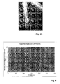
- Figure 4a, 4b and 4c show images obtained from a back side of a semiconductor wafer having embedded features.
- the substrate material of the semiconductor wafer is silicon, and the embedded features are through wafer vias made of copper.
- the three images shown in Figure 4 are obtained at different residual distances of tip ends of the vias from the back surface of the wafer.
- the residual distance d 1 is 6 ⁇ m, and the features visible in the image mostly relate to grinding marks of a grinding tool used in the wafer thinning process.
- a number of image features which might be indicative of the presence of the through wafer vias is low.
- Figure 4b shows an image of a wafer back side where the residual distance d 1 varies between 1 ⁇ m and 2 ⁇ m.
- the features visible in the image include grinding marks similar to those of Figure 4a , and patterns having a structure corresponding to an arrangement pattern of through wafer vias manufactured in the substrate. The features of the grinding pattern and the features of the via pattern are provided in the image with a similar contrast.
- Figure 4c shows an image of the back side of the wafer in which the residual distance d 1 of the vias is less than or equal to 0.5 ⁇ m. It is apparent that the features corresponding to the arrangement of vias is even more prominent than in Figure 4b and that the features corresponding to the arrangement of vias have a higher contrast in the image than the features related to the grinding pattern.
- the image contrast produced by features embedded in the substrate and located below the substrate surface can be enhanced by imposing restrictions to the measuring light used for the imaging. For example, it is desirable that light reflected at the front surface of the substrate or light scattered at structures provided on the front side of the substrate do not contribute to the detected image. Such light travels through the substrate material along a path having a length which is at least two times greater than the thickness of the substrate. Therefore, it is advantageous to select wavelengths of the measuring light contributing to the detected image such that a substantial extinction of measuring light occurs after a path length within the material greater than two times the thickness of the substrate. This can be achieved by selecting the wavelengths such that a penetration depth of the measuring light in the substrate material is smaller than 2.0 times, 1.0 times or 0.5 times a thickness of the substrate. In this context, the penetration depth is defined as the depth at which the intensity of the measuring light inside the substrate material falls to 1/e (about 37%) of the original value at the surface.
- the substrate material is silicon and a thickness of the substrate can be as small as 10 ⁇ m, it is advantageous to use measuring light of wavelengths less than 900 nm, 850 nm, 800 nm or 750 nm, for example.
- the measuring light used for generating an image of an arrangement pattern of features located below a back surface of a substrate should still have a significant intensity when it reaches the buried features. Therefore, it is advantageous to select the wavelengths of the measuring light such that a penetration depth of the measuring light in the substrate is greater than 0.2 times, greater than 0.5 times or greater than 1.5 times a residual distance between the buried features and the substrate surface.
- the substrate material is silicon and where the buried features are through wafer vias made of metal, it is advantageous to use measuring light having wavelengths greater than 500 nm, greater than 550 nm, greater than 600 nm or even greater than 650nm.
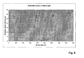
- Figure 6 shows experimental data of the penetration depth in ⁇ m of light in a silicon substrate material in dependence of the wavelength of the light in nm. It is apparent that a lower limit of the wavelength which can be used to detect features more than 1 ⁇ m below the surface should be greater than 500 nm, whereas wavelengths below 900 nm should be used to detect such features in a substrate having a thickness below 35 ⁇ m.
- Figure 5 is a graph of experimental data showing the dependency of the residual distance of the through wafer vias, as shown in Figure 4 , in dependence of a dark field image intensity of arrangement patterns of the vias in the image. From this graph it is apparent that the dark field image intensity and contrast are well-suited to be indicative of the residual thickness.
- the measuring light used for detection can also be selected with respect to its polarization such that a high amount of the incident light enters into the substrate and/or such that the suitably polarized light generates a high image intensity or contrast.
- the optical methods of inspection of a semiconductor wafer can be used for obtaining information used to control a wafer thinning process in mass production of semiconductor devices.
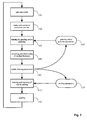
- Such manufacturing method is illustrated with reference to the flowchart shown in Figure 7 below.
- the method includes bonding a first substrate to a second substrate wherein through wafer vias exposed at a back surface of the first substrate are contacted by the second substrate bonded to the first substrate.
- a next wafer is used for processing in a step 101.
- Semiconductor structures and vias are formed on a front side of the wafer by lithographic processes and other processes in a step 103.
- the thinning process may include, for example, grinding and/or polishing.
- the thinning process is controlled by grinding parameters 107, such as, among others, a number of revolutions per unit time of a grinding or polishing apparatus, a force applied between a grinding or polishing tool and the back side of the wafer or a duration of the grinding or polishing process.
- the grinding parameters are selected such that a residual thickness between tip ends of the through wafer vias and the back surface of the wafer is 2 ⁇ m.
- the residual thickness or information indicative of the residual thickness is determined in a step 109 using optical methods as illustrated above.
- the control parameters 107 of the thinning process 105 and control parameters 111 of a subsequent thinning process 113 are updated in a step 115.
- the further thinning process is applied to the back side of the wafer to expose the through wafer vias at the back surface of the wafer in the step 113.
- Such final thinning process may include an etching which selectively removes substrate material and does substantially not remove the material of the through wafer vias.
- the thinning process of step 113 is controlled by process parameters 111 which may include, among others, a duration of the thinning process, a concentration, composition or temperature of an etching substance, or a plasma intensity applied in the thinning process.
- a second substrate is bonded to the wafer in a step 115 after exposing the vias on the back surface.
- the second substrate may comprise a full wafer or individual dyes of semiconductor devices which have been selected according to suitable quality requirements.
- the images obtained from the back surface of the wafer include also other features not related to the through wafer vias. These other features are, for example, generated by defects located on the surface of the substrate. Examples are the grinding marks visible in Figures 4a,4b and 4c . An analysis of such other features can provide information which can be used to control the processing of the wafer. For example the grinding marks can be indicative of a defect of the grinding apparatus used, such that the obtained information may trigger a repair of the grinding apparatus. Moreover, additional images can be obtained in an inspection step by recording one or more images using different wafelengths and polarisations of the measuring light used for imaging.
- the information indicative of the residual thickness of the substrate obtained in step 109 can be used to update control parameters of a thinning process applied to the same wafer subsequently.
- Such process can be referred to as feed-forward control since it is based on information obtained from an individual wafer and is used for controlling further processing of the same wafer.
- the updating of control parameters of the thinning process applied to the individual wafer in step 105 is a feed-back control since it is effective only for a next wafer processed in a production line.
Landscapes
- Physics & Mathematics (AREA)
- Health & Medical Sciences (AREA)
- Life Sciences & Earth Sciences (AREA)
- Chemical & Material Sciences (AREA)
- Analytical Chemistry (AREA)
- Biochemistry (AREA)
- General Health & Medical Sciences (AREA)
- General Physics & Mathematics (AREA)
- Immunology (AREA)
- Pathology (AREA)
- Testing Or Measuring Of Semiconductors Or The Like (AREA)
- Mechanical Treatment Of Semiconductor (AREA)
Priority Applications (4)
| Application Number | Priority Date | Filing Date | Title |
|---|---|---|---|
| EP20100004141 EP2378548A1 (fr) | 2010-04-19 | 2010-04-19 | Procédés de traitement et d'inspection de substrats de semi-conducteur |
| US13/089,127 US8460946B2 (en) | 2010-04-19 | 2011-04-18 | Methods of processing and inspecting semiconductor substrates |
| PCT/EP2011/001992 WO2011131349A1 (fr) | 2010-04-19 | 2011-04-19 | Procédés de traitement et d'inspection de substrats semi-conducteurs |
| TW100113506A TW201203420A (en) | 2010-04-19 | 2011-04-19 | Methods of processing and inspecting semiconductor substrates |
Applications Claiming Priority (1)
| Application Number | Priority Date | Filing Date | Title |
|---|---|---|---|
| EP20100004141 EP2378548A1 (fr) | 2010-04-19 | 2010-04-19 | Procédés de traitement et d'inspection de substrats de semi-conducteur |
Publications (1)
| Publication Number | Publication Date |
|---|---|
| EP2378548A1 true EP2378548A1 (fr) | 2011-10-19 |
Family
ID=42455426
Family Applications (1)
| Application Number | Title | Priority Date | Filing Date |
|---|---|---|---|
| EP20100004141 Withdrawn EP2378548A1 (fr) | 2010-04-19 | 2010-04-19 | Procédés de traitement et d'inspection de substrats de semi-conducteur |
Country Status (4)
| Country | Link |
|---|---|
| US (1) | US8460946B2 (fr) |
| EP (1) | EP2378548A1 (fr) |
| TW (1) | TW201203420A (fr) |
| WO (1) | WO2011131349A1 (fr) |
Cited By (3)
| Publication number | Priority date | Publication date | Assignee | Title |
|---|---|---|---|---|
| DE102012002129A1 (de) * | 2012-02-03 | 2013-08-08 | Hq-Dielectrics Gmbh | Verfahren und vorrichtung zum freilegen von in einem halbleiter-substrat ausgebildeten durchkontaktierungen |
| WO2017160344A1 (fr) * | 2016-03-15 | 2017-09-21 | Raytheon Company | Structures de surveillance in situ et procédés d'utilisation dans un traitement à semi-conducteurs |
| CN108695184A (zh) * | 2017-03-31 | 2018-10-23 | Imec 非营利协会 | 用于半导体制造工艺的度量方法 |
Families Citing this family (5)
| Publication number | Priority date | Publication date | Assignee | Title |
|---|---|---|---|---|
| FR2994734B1 (fr) * | 2012-08-21 | 2017-08-25 | Fogale Nanotech | Dispositif et procede pour faire des mesures dimensionnelles sur des objets multi-couches tels que des wafers. |
| KR102144539B1 (ko) * | 2014-11-05 | 2020-08-18 | 주식회사 히타치엘지 데이터 스토리지 코리아 | 거리 측정 장치 |
| JP6560147B2 (ja) * | 2016-03-07 | 2019-08-14 | ルネサスエレクトロニクス株式会社 | 半導体装置の製造方法 |
| US10133838B2 (en) * | 2017-01-30 | 2018-11-20 | Dongfang Jingyuan Electron Limited | Guided defect detection of integrated circuits |
| US11640118B2 (en) * | 2020-08-17 | 2023-05-02 | Tokyo Electron Limited | Method of pattern alignment for field stitching |
Citations (10)
| Publication number | Priority date | Publication date | Assignee | Title |
|---|---|---|---|---|
| US4933567A (en) * | 1988-07-13 | 1990-06-12 | Vti, Inc. | Method and apparatus for nondestructively measuring subsurface defects in materials |
| US6916725B2 (en) | 2003-01-24 | 2005-07-12 | Seiko Epson Corporation | Method for manufacturing semiconductor device, and method for manufacturing semiconductor module |
| US20050158889A1 (en) | 2000-02-29 | 2005-07-21 | Brouillette Donald W. | Wafer thickness control during backside grind |
| US7214615B2 (en) | 2003-03-17 | 2007-05-08 | Seiko Epson Corporation | Method of manufacturing semiconductor device, semiconductor device, circuit substrate and electronic apparatus |
| US20090008794A1 (en) * | 2007-07-03 | 2009-01-08 | Weng-Jin Wu | Thickness Indicators for Wafer Thinning |
| US20090227047A1 (en) * | 2008-03-06 | 2009-09-10 | Taiwan Semiconductor Manufacturing Co., Ltd. | Method and apparatus for thinning a substrate |
| WO2009121628A2 (fr) | 2008-04-04 | 2009-10-08 | Nanda Technologies Gmbh | Système et procédé de contrôle optique |
| US20100032764A1 (en) | 2008-08-08 | 2010-02-11 | Paul Stephen Andry | Through silicon via and method of fabricating same |
| US20100041226A1 (en) | 2008-08-18 | 2010-02-18 | Novellus Systems, Inc. | Process For Through Silicon Via Filing |
| US20100038800A1 (en) | 2008-08-18 | 2010-02-18 | Samsung Electronics Co., Ltd. | Through-silicon via structures including conductive protective layers and methods of forming the same |
Family Cites Families (5)
| Publication number | Priority date | Publication date | Assignee | Title |
|---|---|---|---|---|
| US6673637B2 (en) * | 2000-09-20 | 2004-01-06 | Kla-Tencor Technologies | Methods and systems for determining a presence of macro defects and overlay of a specimen |
| US7115858B1 (en) | 2000-09-25 | 2006-10-03 | Nanometrics Incorporated | Apparatus and method for the measurement of diffracting structures |
| US6788416B2 (en) * | 2002-05-22 | 2004-09-07 | Texas Instruments Incorporated | Method and apparatus for dynamic DMD testing |
| US7563714B2 (en) * | 2006-01-13 | 2009-07-21 | International Business Machines Corporation | Low resistance and inductance backside through vias and methods of fabricating same |
| JP2007266557A (ja) * | 2006-03-30 | 2007-10-11 | Renesas Technology Corp | 半導体装置の製造方法 |
-
2010
- 2010-04-19 EP EP20100004141 patent/EP2378548A1/fr not_active Withdrawn
-
2011
- 2011-04-18 US US13/089,127 patent/US8460946B2/en not_active Expired - Fee Related
- 2011-04-19 TW TW100113506A patent/TW201203420A/zh unknown
- 2011-04-19 WO PCT/EP2011/001992 patent/WO2011131349A1/fr not_active Ceased
Patent Citations (10)
| Publication number | Priority date | Publication date | Assignee | Title |
|---|---|---|---|---|
| US4933567A (en) * | 1988-07-13 | 1990-06-12 | Vti, Inc. | Method and apparatus for nondestructively measuring subsurface defects in materials |
| US20050158889A1 (en) | 2000-02-29 | 2005-07-21 | Brouillette Donald W. | Wafer thickness control during backside grind |
| US6916725B2 (en) | 2003-01-24 | 2005-07-12 | Seiko Epson Corporation | Method for manufacturing semiconductor device, and method for manufacturing semiconductor module |
| US7214615B2 (en) | 2003-03-17 | 2007-05-08 | Seiko Epson Corporation | Method of manufacturing semiconductor device, semiconductor device, circuit substrate and electronic apparatus |
| US20090008794A1 (en) * | 2007-07-03 | 2009-01-08 | Weng-Jin Wu | Thickness Indicators for Wafer Thinning |
| US20090227047A1 (en) * | 2008-03-06 | 2009-09-10 | Taiwan Semiconductor Manufacturing Co., Ltd. | Method and apparatus for thinning a substrate |
| WO2009121628A2 (fr) | 2008-04-04 | 2009-10-08 | Nanda Technologies Gmbh | Système et procédé de contrôle optique |
| US20100032764A1 (en) | 2008-08-08 | 2010-02-11 | Paul Stephen Andry | Through silicon via and method of fabricating same |
| US20100041226A1 (en) | 2008-08-18 | 2010-02-18 | Novellus Systems, Inc. | Process For Through Silicon Via Filing |
| US20100038800A1 (en) | 2008-08-18 | 2010-02-18 | Samsung Electronics Co., Ltd. | Through-silicon via structures including conductive protective layers and methods of forming the same |
Non-Patent Citations (2)
| Title |
|---|
| ABT I ET AL: "Characterization of silicon microstrip detectors using an infrared laser system", NUCLEAR INSTRUMENTS & METHODS IN PHYSICS RESEARCH. SECTION A: ACCELERATORS, SPECTROMETERS, DETECTORS, AND ASSOCIATED EQUIPMENT, ELSEVIER BV * NORTH-HOLLAND, NETHERLANDS, vol. 423, no. 2-3, 1 March 1999 (1999-03-01), pages 303 - 319, XP004160862, ISSN: 0168-9002, DOI: 10.1016/S0168-9002(98)01337-0 * |
| ANNE JOURDAIN ET AL.: "New Hybrid Bonding Approach for 3D Stacking of ICs", CHIP SCALE REVIEW, August 2009 (2009-08-01), pages 24 - 28 |
Cited By (5)
| Publication number | Priority date | Publication date | Assignee | Title |
|---|---|---|---|---|
| DE102012002129A1 (de) * | 2012-02-03 | 2013-08-08 | Hq-Dielectrics Gmbh | Verfahren und vorrichtung zum freilegen von in einem halbleiter-substrat ausgebildeten durchkontaktierungen |
| WO2017160344A1 (fr) * | 2016-03-15 | 2017-09-21 | Raytheon Company | Structures de surveillance in situ et procédés d'utilisation dans un traitement à semi-conducteurs |
| US10236226B2 (en) | 2016-03-15 | 2019-03-19 | Raytheon Company | In-situ calibration structures and methods of use in semiconductor processing |
| CN108695184A (zh) * | 2017-03-31 | 2018-10-23 | Imec 非营利协会 | 用于半导体制造工艺的度量方法 |
| CN108695184B (zh) * | 2017-03-31 | 2023-04-28 | Imec 非营利协会 | 用于半导体制造工艺的度量方法 |
Also Published As
| Publication number | Publication date |
|---|---|
| TW201203420A (en) | 2012-01-16 |
| US8460946B2 (en) | 2013-06-11 |
| US20120094401A1 (en) | 2012-04-19 |
| WO2011131349A1 (fr) | 2011-10-27 |
Similar Documents
| Publication | Publication Date | Title |
|---|---|---|
| US8460946B2 (en) | Methods of processing and inspecting semiconductor substrates | |
| KR100516405B1 (ko) | 웨이퍼의 에지 노광 영역 검사 장치 | |
| US9305341B2 (en) | System and method for measurement of through silicon structures | |
| JP4759228B2 (ja) | 反射率測定によるエッジビード除去の検査 | |
| KR20190049890A (ko) | 반도체 웨이퍼 검사를 위한 결함 마킹 | |
| WO2017123467A1 (fr) | Systèmes et méthodes permettant une ellipsométrie spectroscopique infrarouge étendue | |
| WO2007146798A2 (fr) | Procédés et systèmes pour détecter des défauts sur un spéciment en utilisant une combinaison de données de canal de champ clair et de données de canal de champ sombre | |
| WO2009074984A2 (fr) | Système optique et procédé pour la mesure d'un ou de plusieurs paramètres de trous d'interconnexion | |
| US20170138868A1 (en) | Optical method and system for defects detection in three-dimensional structures | |
| US6885446B2 (en) | Method and system for monitoring a process of material removal from the surface of a patterned structure | |
| JP4606443B2 (ja) | 荷電粒子線を用いた回路パターン用基板検査方法および基板検査装置 | |
| TW202532837A (zh) | 用於偵測封裝中的缺陷的方法及設備 | |
| US7440094B2 (en) | Optical sample characterization system | |
| US20140113526A1 (en) | Wafer process control | |
| KR100638965B1 (ko) | 금속 잔류물 검사 장비 및 방법 | |
| US20150168132A1 (en) | Method and system for use in optical measurements in deep three-dimensional structures | |
| KR102790734B1 (ko) | 다중 수집 채널로부터의 정보의 결합에 의한 디자인 대 웨이퍼 이미지 상관 관계 | |
| TWI829958B (zh) | 用於檢驗半導體裝置之系統及方法 | |
| US9423359B2 (en) | Wafer charging electromagnetic inspection tool and method of using | |
| JP7759412B2 (ja) | レーザアニールパターンの抑制 | |
| US20080151259A1 (en) | Synchronized wafer mapping | |
| KR100694597B1 (ko) | 반도체 장치에서 패턴 결함 검출 방법 | |
| US12590900B2 (en) | Wafer inspection apparatus using three-dimensional image and method of inspecting wafer using the same | |
| US20240353321A1 (en) | Combined Spectroscopic Reflectometry And Pattern Recognition Based Measurements Of Semiconductor Structures | |
| KR20250119522A (ko) | 샘플 기판 내부의 결함 있는 접합 계면 검출을 위한 검사 방법 및 그 검사 방법을 구현하는 측정 시스템 |
Legal Events
| Date | Code | Title | Description |
|---|---|---|---|
| 17P | Request for examination filed |
Effective date: 20110329 |
|
| AK | Designated contracting states |
Kind code of ref document: A1 Designated state(s): AT BE BG CH CY CZ DE DK EE ES FI FR GB GR HR HU IE IS IT LI LT LU LV MC MK MT NL NO PL PT RO SE SI SK SM TR |
|
| AX | Request for extension of the european patent |
Extension state: AL BA ME RS |
|
| PUAI | Public reference made under article 153(3) epc to a published international application that has entered the european phase |
Free format text: ORIGINAL CODE: 0009012 |
|
| RIC1 | Information provided on ipc code assigned before grant |
Ipc: H01L 21/66 20060101ALI20150224BHEP Ipc: H01L 21/768 20060101ALI20150224BHEP Ipc: G01N 21/95 20060101AFI20150224BHEP |
|
| GRAP | Despatch of communication of intention to grant a patent |
Free format text: ORIGINAL CODE: EPIDOSNIGR1 |
|
| INTG | Intention to grant announced |
Effective date: 20150518 |
|
| STAA | Information on the status of an ep patent application or granted ep patent |
Free format text: STATUS: THE APPLICATION IS DEEMED TO BE WITHDRAWN |
|
| 18D | Application deemed to be withdrawn |
Effective date: 20150929 |