EP2378555B1 - Dispositif électroluminescent - Google Patents
Dispositif électroluminescent Download PDFInfo
- Publication number
- EP2378555B1 EP2378555B1 EP11157948.8A EP11157948A EP2378555B1 EP 2378555 B1 EP2378555 B1 EP 2378555B1 EP 11157948 A EP11157948 A EP 11157948A EP 2378555 B1 EP2378555 B1 EP 2378555B1
- Authority
- EP
- European Patent Office
- Prior art keywords
- light emitting
- electrode
- emitting device
- layer
- semiconductor layer
- Prior art date
- Legal status (The legal status is an assumption and is not a legal conclusion. Google has not performed a legal analysis and makes no representation as to the accuracy of the status listed.)
- Active
Links
Images


Classifications
-
- H—ELECTRICITY
- H10—SEMICONDUCTOR DEVICES; ELECTRIC SOLID-STATE DEVICES NOT OTHERWISE PROVIDED FOR
- H10H—INORGANIC LIGHT-EMITTING SEMICONDUCTOR DEVICES HAVING POTENTIAL BARRIERS
- H10H29/00—Integrated devices, or assemblies of multiple devices, comprising at least one light-emitting semiconductor element covered by group H10H20/00
- H10H29/10—Integrated devices comprising at least one light-emitting semiconductor component covered by group H10H20/00
-
- H—ELECTRICITY
- H10—SEMICONDUCTOR DEVICES; ELECTRIC SOLID-STATE DEVICES NOT OTHERWISE PROVIDED FOR
- H10D—INORGANIC ELECTRIC SEMICONDUCTOR DEVICES
- H10D30/00—Field-effect transistors [FET]
- H10D30/60—Insulated-gate field-effect transistors [IGFET]
-
- H—ELECTRICITY
- H10—SEMICONDUCTOR DEVICES; ELECTRIC SOLID-STATE DEVICES NOT OTHERWISE PROVIDED FOR
- H10H—INORGANIC LIGHT-EMITTING SEMICONDUCTOR DEVICES HAVING POTENTIAL BARRIERS
- H10H20/00—Individual inorganic light-emitting semiconductor devices having potential barriers, e.g. light-emitting diodes [LED]
- H10H20/80—Constructional details
- H10H20/83—Electrodes
- H10H20/831—Electrodes characterised by their shape
- H10H20/8314—Electrodes characterised by their shape extending at least partially onto an outer side surface of the bodies
-
- H—ELECTRICITY
- H10—SEMICONDUCTOR DEVICES; ELECTRIC SOLID-STATE DEVICES NOT OTHERWISE PROVIDED FOR
- H10H—INORGANIC LIGHT-EMITTING SEMICONDUCTOR DEVICES HAVING POTENTIAL BARRIERS
- H10H20/00—Individual inorganic light-emitting semiconductor devices having potential barriers, e.g. light-emitting diodes [LED]
- H10H20/80—Constructional details
- H10H20/84—Coatings, e.g. passivation layers or antireflective coatings
- H10H20/841—Reflective coatings, e.g. dielectric Bragg reflectors
-
- H—ELECTRICITY
- H10—SEMICONDUCTOR DEVICES; ELECTRIC SOLID-STATE DEVICES NOT OTHERWISE PROVIDED FOR
- H10H—INORGANIC LIGHT-EMITTING SEMICONDUCTOR DEVICES HAVING POTENTIAL BARRIERS
- H10H20/00—Individual inorganic light-emitting semiconductor devices having potential barriers, e.g. light-emitting diodes [LED]
- H10H20/80—Constructional details
- H10H20/85—Packages
- H10H20/857—Interconnections, e.g. lead-frames, bond wires or solder balls
-
- H—ELECTRICITY
- H10—SEMICONDUCTOR DEVICES; ELECTRIC SOLID-STATE DEVICES NOT OTHERWISE PROVIDED FOR
- H10H—INORGANIC LIGHT-EMITTING SEMICONDUCTOR DEVICES HAVING POTENTIAL BARRIERS
- H10H20/00—Individual inorganic light-emitting semiconductor devices having potential barriers, e.g. light-emitting diodes [LED]
- H10H20/80—Constructional details
- H10H20/81—Bodies
- H10H20/819—Bodies characterised by their shape, e.g. curved or truncated substrates
- H10H20/82—Roughened surfaces, e.g. at the interface between epitaxial layers
Definitions
- each layer shown in the drawings may be exaggerated, omitted or schematically drawn for the purpose of convenience or clarity.
- the size of elements does not utterly reflect an actual size.
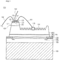
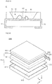
- the first electrode 160 supports a plurality of layers formed thereon and has a function of an electrode.
- the first electrode 160 may include a support member having conductivity.
- the adhesive layer 158 may be formed on the first electrode 160.
- the adhesive layer 158 is a bonding layer formed under the reflective layer 157. Outer side surfaces of the adhesive layer 158 are exposed and the adhesive layer 158 makes contact with the reflective layer 157 to serve as a mediator for reinforcing the bonding strength between the first electrode 160 and the reflective layer 157.
- the protective member 155 may include a metal having superior adhesive property.
- the protective member 155 may include at least one selected from the group consisting of Ti, Ni, Pt, Pd, Rh, Ir and W.
- the protective member 155 may reinforce the adhesive strength between the light emitting structure 145 and the reflective layer 157, so that the reliability of the light emitting device 100 can be improved.
- the protective member 155 may not be broken or fragments of the protective member 155 may not be generated when the laser scribing process or the laser lift off (LLO) process is performed to break a plurality of chips into individual chip units, so that the reliability of the light emitting device 100 can be improved.
- LLO laser lift off
- the protective member 155 may include a material having electric insulating property.
- the protective member 155 may include at least one selected from the group consisting of Si0 2 , Si x O y , Si 3 N 4 , Si x N y , SiO x N y , Al 2 O 3 , TiO 2 , ITO, AZO, and ZnO.
- the reflective layer 157 may be formed on the adhesive layer 158.
- the reflective layer 157 reflects light incident from the light emitting structure 145, thereby improving the light extraction efficiency of the light emitting device 100.
- the undoped semiconductor layer is not doped with conductive dopant, so the undoped semiconductor layer has electric conductivity remarkably lower than that of the n type semiconductor layer or the second conductive semiconductor layer 130.
- the undoped semiconductor layer is grown to improve crystalline property of the second conductive semiconductor layer 130.
- the doping concentration of the conductive dopant in the first and second conductive semiconductor layers 150 and 130 may be uniform or non-uniform. That is, the light emitting structure 145 may have various structures, and the embodiment may not limit the structure of the light emitting structure 145.
- the control switch 120 can be formed on the top surface of the second conductive semiconductor layer 130 of the light emitting structure 145 through a simple process.
- the control switch 120 can be formed with a fine size by doping silicon in the semiconductor manufacturing process, so the control switch 120 may not degrade the light emitting efficiency of the light emitting device 100.
- control switch 120 is connected to the light emitting structure 145 in series.
- the control switch 120 may include a semiconductor switch, such as a JFET switch, a CMOS switch, or a BJT switch, which controls the light emitting structure 145 according to the control signal G applied to the gate electrode 127.
- FIGS. 4 to 12 are sectional views showing the method of manufacturing the light emitting device according to the first embodiment.
- the adhesive layer 158 is formed on the reflective layer 157 and the protective member 155, and the first electrode 160 is formed on the adhesive layer 158.
- the first electrode 160 may include the support member having conductivity.
- the first electrode 160 may include at least one of Ti, Cr, Ni, Al, Pt, Au, W, Cu, Mo, and a semiconductor substrate doped with impurities.
- the LLO (laser lift off) process which may reduce the product yield of the light emitting device, can be omitted, so that the reliability of the manufacturing process for the light emitting device 100 can be improved.
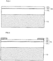
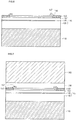
- the sapphire substrate can be employed as a base substrate of the light emitting structure 145 instead of the silicon substrate.
- the sapphire substrate is selectively removed through the LLO process and the body is formed 121 on the light emitting structure 145 through the deposition process, but the embodiment is not limited thereto.
- the gate insulating layer 126 is formed such that the gate insulating layer 126 makes contact with the body 121, the source region 122 and the drain region 123, and the gate electrode 127 is formed on the gate insulating layer 126.
- the source electrode 124 is formed on the source region and the drain electrode 125 is formed on the drain region 123, thereby forming the control switch 120.
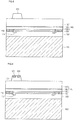
- the light emitting device chips can be divided into individual chip units through the isolation etching.
- the isolation etching may include a dry etching, such as an ICP (inductively coupled plasma) etching.
- ICP inductively coupled plasma
- the second electrode 170 can be formed through the CVD, E-beam evaporation or sputtering.
- a wire interconnection is formed to allow the control switch 120 to serve as a switch.
- Such a wire interconnection can be formed after the light emitting device 100 has been mounted on the substrate, but the embodiment is not limited thereto.
- one of the source electrode 124 and the drain electrode 125 is electrically connected to the second electrode 170 formed on the light emitting structure 145 through the first wire 181 and the other of the source electrode 124 and the drain electrode 125 is connected to the external power source by a second wire 182.
- another external power source can be connected to the gate electrode 127 through a third wire 183 to supply the control signal.
- the light emitting device 100B includes a first electrode 160, an adhesive layer 158 on the first electrode 160, a protective member 155 on the first electrode 160 or on an outer peripheral region of a top surface of the adhesive layer 158, a reflective layer 157 on the adhesive layer 158, an ohmic contact layer 156 on the reflective layer 157, a light emitting structure 145 on the protective member 155 and the ohmic contact layer 156, a control switch 120 on the light emitting structure 145, and a second electrode 171 formed on the control switch 120 and the light emitting structure 145 to electrically connect the control switch 120 to the light emitting structure 145.
- the insulating layer 175 may include at lest one selected from the group consisting of Si0 2 , Si x O y , Si 3 N 4 , Si x N y , SiO x N y , Al 2 O 3 and TiO 2 .
- the wires can be omitted in the light emitting device 100B according to the second embodiment by forming the second electrode 171.
- the light may not interference with the wires.
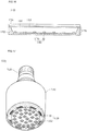
- FIG. 14 is a sectional view showing a light emitting device package including the light emitting device according to the embodiments.
- the light emitting device package 30 includes a package body 20, first to third lead electrodes 31 to 33 formed on the package body 20, the light emitting device 100 provided on the package body 20 to receive power from the first and second lead electrodes 31 and 32 and the control signal from the third lead electrode 33, and a molding member 40 that surrounds the light emitting device 100.
- the first to third lead electrodes 31 to 33 are electrically isolated from each other. For instance, the power is supplied to the first and third lead electrodes 31 and 33 and the control signal is supplied to the second electrode 32.
- the first and second lead electrodes 31 and 32 may extend by passing through the package body 20.
- one ends of the first and second lead electrodes 31 and 32 are disposed in the cavity 50 and the other ends of the first and second electrodes 31 and 32 are attached to an outer surface of the package body 20 and exposed to the outside.
Landscapes
- Led Devices (AREA)
- Led Device Packages (AREA)
- Non-Portable Lighting Devices Or Systems Thereof (AREA)
Claims (11)
- Dispositif électroluminescent comprenant :une première électrode (160) ;une structure électroluminescente (145) incluant une première couche semi-conductrice (150), une couche active (140) et une seconde couche semi-conductrice (130) sur la première électrode (160) ;une seconde électrode (171) sur la structure électroluminescente (145) ; etun commutateur de commande (120) sur la structure électroluminescente (145) pour commander la structure électroluminescente,dans lequel le commutateur de commande (120) inclut :un corps (121) composé d'un matériau de silicium et incluant un premier dopant ;des régions de source et de drain (122, 123) incluant un second dopant sur le corps (121) ;une couche d'isolation de grille (126) sur le corps (121) entre les régions de source et de drain (122, 123) ; etune électrode de grille (127) sur la couche d'isolation de grille (126),dans lequel le corps (121) du commutateur de commande est disposé sur la seconde couche semi-conductrice (130) et la première électrode (160) est disposée sur la première couche semi-conductrice (150),dans lequel la seconde électrode (171) s'étend depuis la seconde couche semi-conductrice (130) de manière à être électriquement connectée à l'une des régions de source et de drain (122, 123),dans lequel une extrémité de la seconde électrode (171) est électriquement connectée à la seconde couche semi-conductrice (130) et l'autre extrémité de la seconde électrode (171) est électriquement connectée à l'une des régions de source et de drain (122, 123),dans lequel la seconde couche semi-conductrice (130) comprend un motif de rugosité de celle-ci,dans lequel une surface de contact entre l'une extrémité de la seconde électrode (171) et la seconde couche semi-conductrice (130) est inférieure à une surface du motif de rugosité.
- Dispositif électroluminescent selon la revendication 1, dans lequel le commutateur de commande (120) commande une opération de la structure électroluminescente (145) en réponse à un signal de commande.
- Dispositif électroluminescent selon la revendication 2, dans lequel le signal de commande inclut l'un d'un signal de commande on/off et d'un signal de commande d'échelle de gris.
- Dispositif électroluminescent selon l'une quelconque des revendications précédentes, dans lequel le commutateur de commande (120) est formé au niveau d'une région périphérique extérieure de la structure électroluminescente (145).
- Dispositif électroluminescent selon l'une quelconque des revendications précédentes, dans lequel la couche d'isolation de grille (126) est disposée sur une surface supérieure du corps (121).
- Dispositif électroluminescent selon l'une quelconque des revendications précédentes, dans lequel le premier dopant a la même polarité que la première couche semi-conductrice (150).
- Dispositif électroluminescent selon l'une quelconque des revendications précédentes, dans lequel le second dopant a la même polarité que la seconde couche semi-conductrice (130).
- Dispositif électroluminescent selon l'une quelconque des revendications précédentes, comprenant en outre des électrodes de source et de drain (124, 125) sur les régions de source et de drain (122, 123), respectivement.
- Dispositif électroluminescent selon l'une quelconque des revendications précédentes, dans lequel la seconde électrode (171) n'est pas verticalement recouverte du motif de rugosité.
- Dispositif électroluminescent selon l'une quelconque des revendications précédentes, comprenant en outre au moins l'une d'une couche réfléchissante (157) et d'une couche de contact ohmique (156) entre la première électrode (150) et la structure électroluminescente (145).
- Dispositif électroluminescent selon l'une quelconque des revendications précédentes, comprenant en outre une couche d'isolation (175) entre la seconde électrode (171) et un côté latéral du corps (121).
Applications Claiming Priority (1)
| Application Number | Priority Date | Filing Date | Title |
|---|---|---|---|
| KR1020100033835A KR101007125B1 (ko) | 2010-04-13 | 2010-04-13 | 발광 소자, 발광 소자 제조방법 및 발광 소자 패키지 |
Publications (3)
| Publication Number | Publication Date |
|---|---|
| EP2378555A2 EP2378555A2 (fr) | 2011-10-19 |
| EP2378555A3 EP2378555A3 (fr) | 2015-12-30 |
| EP2378555B1 true EP2378555B1 (fr) | 2019-06-12 |
Family
ID=43616042
Family Applications (1)
| Application Number | Title | Priority Date | Filing Date |
|---|---|---|---|
| EP11157948.8A Active EP2378555B1 (fr) | 2010-04-13 | 2011-03-11 | Dispositif électroluminescent |
Country Status (6)
| Country | Link |
|---|---|
| US (2) | US8872215B2 (fr) |
| EP (1) | EP2378555B1 (fr) |
| JP (1) | JP5897813B2 (fr) |
| KR (1) | KR101007125B1 (fr) |
| CN (1) | CN102222741B (fr) |
| TW (1) | TWI553908B (fr) |
Families Citing this family (14)
| Publication number | Priority date | Publication date | Assignee | Title |
|---|---|---|---|---|
| US20150069380A1 (en) * | 2011-12-12 | 2015-03-12 | Raghvendra K. Pandey | Varistor-transistor hybrid devices |
| US9153732B2 (en) * | 2012-02-23 | 2015-10-06 | Nthdegree Technologies Worldwide Inc. | Active LED module |
| CN103489965A (zh) * | 2012-06-13 | 2014-01-01 | 联胜光电股份有限公司 | 具反射镜保护层的发光二极管 |
| DE102012111247A1 (de) | 2012-11-21 | 2014-05-22 | Osram Opto Semiconductors Gmbh | Optoelektronisches Halbleiterbauteil |
| US9177992B2 (en) | 2013-01-09 | 2015-11-03 | Nthdegree Technologies Worldwide Inc. | Active LED module with LED and transistor formed on same substrate |
| US10663142B2 (en) * | 2014-03-31 | 2020-05-26 | Bridgelux Inc. | Light-emitting device with reflective ceramic substrate |
| DE102015110496B4 (de) | 2015-06-30 | 2018-06-14 | Infineon Technologies Dresden Gmbh | Integriertes, lichtemittierendes bauelement,integriertes sensorbauelement undherstellungsverfahren |
| TWI697076B (zh) * | 2016-01-13 | 2020-06-21 | 晶元光電股份有限公司 | 發光元件及其製造方法 |
| KR20180078941A (ko) * | 2016-12-30 | 2018-07-10 | (재)한국나노기술원 | 액티브 매트릭스 디스플레이용 led 소자 및 그의 제조방법 |
| JP2019161172A (ja) * | 2018-03-16 | 2019-09-19 | 株式会社ブイ・テクノロジー | Led・トランジスタ複合素子 |
| US10201051B1 (en) * | 2018-04-10 | 2019-02-05 | Nthdegree Technologies Worldwide Inc. | Active LED module with LED and vertical MOS transistor formed on same substrate |
| CN114005376A (zh) * | 2020-07-27 | 2022-02-01 | 北京芯海视界三维科技有限公司 | 发光模组及显示器件 |
| JP7510596B2 (ja) * | 2020-10-30 | 2024-07-04 | 日亜化学工業株式会社 | 発光装置及びその製造方法 |
| CN116266603B (zh) * | 2021-12-17 | 2026-04-03 | 山东浪潮华光光电子股份有限公司 | 一种具有自恒流功能的发光二极管及其制备方法 |
Citations (2)
| Publication number | Priority date | Publication date | Assignee | Title |
|---|---|---|---|---|
| JPH0341769A (ja) * | 1989-07-07 | 1991-02-22 | Nippon Telegr & Teleph Corp <Ntt> | 光電子集積回路及びその製法 |
| JP2001127278A (ja) * | 1999-10-25 | 2001-05-11 | Rohm Co Ltd | 複合半導体装置 |
Family Cites Families (27)
| Publication number | Priority date | Publication date | Assignee | Title |
|---|---|---|---|---|
| US4152711A (en) * | 1976-04-01 | 1979-05-01 | Mitsubishi Denki Kabuchiki Kaisha | Semiconductor controlled luminescent device |
| JPS5728375A (en) * | 1980-07-28 | 1982-02-16 | Fujitsu Ltd | Manufacture of semiconductor device |
| US4388633A (en) * | 1980-09-29 | 1983-06-14 | Hughes Aircraft Company | Monolithic transistor coupled electroluminescent diode |
| JPS5917189A (ja) * | 1982-07-20 | 1984-01-28 | Citizen Watch Co Ltd | 電子時計 |
| JPS59171189A (ja) | 1984-01-17 | 1984-09-27 | Hitachi Ltd | 半導体発光素子 |
| US4704369A (en) * | 1985-04-01 | 1987-11-03 | Energy Conversion Devices, Inc. | Method of severing a semiconductor device |
| EP0233725B1 (fr) * | 1986-02-18 | 1995-04-19 | Kabushiki Kaisha Toshiba | Dispositif opto-electronique et procédé pour sa fabrication |
| EP0406506A1 (fr) * | 1989-07-07 | 1991-01-09 | International Business Machines Corporation | Dispositif semi-conducteur optoélectronique électroluminescent |
| JP3016302B2 (ja) * | 1992-04-23 | 2000-03-06 | 日本電気株式会社 | pnpn半導体素子とその駆動回路 |
| US6040590A (en) * | 1996-12-12 | 2000-03-21 | California Institute Of Technology | Semiconductor device with electrostatic control |
| US6274890B1 (en) * | 1997-01-15 | 2001-08-14 | Kabushiki Kaisha Toshiba | Semiconductor light emitting device and its manufacturing method |
| JP2003086784A (ja) * | 2001-09-13 | 2003-03-20 | Furukawa Electric Co Ltd:The | GaN系半導体装置 |
| JP3946062B2 (ja) * | 2002-03-18 | 2007-07-18 | シャープ株式会社 | 表示装置およびその製造方法 |
| JP5077282B2 (ja) | 2002-08-30 | 2012-11-21 | 日亜化学工業株式会社 | 発光素子搭載用パッケージおよび発光装置 |
| KR20040076330A (ko) * | 2003-02-25 | 2004-09-01 | 삼성전자주식회사 | 실리콘 광소자 및 이를 적용한 광신호 입출력장치 |
| EP1733492A2 (fr) | 2004-03-11 | 2006-12-20 | i2Telecom International, Inc. | Adaptation de vitesse dynamique d'emission de paquets de communications vocales en temps reel a la bande passante disponible |
| US20080128727A1 (en) * | 2004-09-10 | 2008-06-05 | Luminus Devices, Inc. | Light recycling systems and methods |
| GB0422913D0 (en) * | 2004-10-15 | 2004-11-17 | Elam T Ltd | Electroluminescent devices |
| EP2005488B1 (fr) * | 2005-12-16 | 2013-07-31 | Samsung Display Co., Ltd. | Dispositif optique et procédé de fabrication |
| KR100788545B1 (ko) | 2006-12-29 | 2007-12-26 | 삼성에스디아이 주식회사 | 유기 전계 발광 표시 장치 및 그 제조 방법 |
| JP4954725B2 (ja) | 2007-01-23 | 2012-06-20 | 三菱電機株式会社 | 発光素子駆動装置およびそれを用いた表示装置 |
| JP2008288179A (ja) | 2007-05-16 | 2008-11-27 | Denshi System Design Kk | 発光ダイオードの点灯制御方法及び制御回路 |
| US7759670B2 (en) * | 2007-06-12 | 2010-07-20 | SemiLEDs Optoelectronics Co., Ltd. | Vertical LED with current guiding structure |
| US9136498B2 (en) * | 2007-06-27 | 2015-09-15 | Qd Vision, Inc. | Apparatus and method for modulating photon output of a quantum dot light emitting device |
| CN101257075B (zh) * | 2008-03-13 | 2010-05-12 | 鹤山丽得电子实业有限公司 | 一种发光二极管器件及其制造方法 |
| JP2009266855A (ja) | 2008-04-22 | 2009-11-12 | Toshiba Lighting & Technology Corp | Led照明装置 |
| TWI573185B (zh) * | 2009-05-12 | 2017-03-01 | 美國伊利諾大學理事會 | 用於可變形及半透明顯示器之超薄微刻度無機發光二極體之印刷總成 |
-
2010
- 2010-04-13 KR KR1020100033835A patent/KR101007125B1/ko not_active Expired - Fee Related
-
2011
- 2011-01-28 TW TW100103329A patent/TWI553908B/zh not_active IP Right Cessation
- 2011-02-23 US US13/033,224 patent/US8872215B2/en active Active
- 2011-03-11 EP EP11157948.8A patent/EP2378555B1/fr active Active
- 2011-03-11 CN CN201110062313.6A patent/CN102222741B/zh active Active
- 2011-04-06 JP JP2011084693A patent/JP5897813B2/ja not_active Expired - Fee Related
-
2014
- 2014-10-01 US US14/503,906 patent/US9281342B2/en not_active Expired - Fee Related
Patent Citations (2)
| Publication number | Priority date | Publication date | Assignee | Title |
|---|---|---|---|---|
| JPH0341769A (ja) * | 1989-07-07 | 1991-02-22 | Nippon Telegr & Teleph Corp <Ntt> | 光電子集積回路及びその製法 |
| JP2001127278A (ja) * | 1999-10-25 | 2001-05-11 | Rohm Co Ltd | 複合半導体装置 |
Also Published As
| Publication number | Publication date |
|---|---|
| US20150014734A1 (en) | 2015-01-15 |
| KR101007125B1 (ko) | 2011-01-10 |
| EP2378555A3 (fr) | 2015-12-30 |
| JP2011222999A (ja) | 2011-11-04 |
| TW201135979A (en) | 2011-10-16 |
| CN102222741A (zh) | 2011-10-19 |
| US8872215B2 (en) | 2014-10-28 |
| CN102222741B (zh) | 2014-08-27 |
| EP2378555A2 (fr) | 2011-10-19 |
| US20110248302A1 (en) | 2011-10-13 |
| US9281342B2 (en) | 2016-03-08 |
| JP5897813B2 (ja) | 2016-03-30 |
| TWI553908B (zh) | 2016-10-11 |
Similar Documents
| Publication | Publication Date | Title |
|---|---|---|
| US10833226B2 (en) | Light emitting device and light emitting device package | |
| EP2378555B1 (fr) | Dispositif électroluminescent | |
| EP2432036B1 (fr) | Diode électroluminescente | |
| EP2381491B1 (fr) | Diode électroluminescente | |
| EP2562815B1 (fr) | Dispositif électroluminescent et emballage de dispositif électroluminescent | |
| EP2312631B1 (fr) | Dispositif électroluminescent et emballage de dispositif électroluminescent doté de celui-ci | |
| EP2381489B1 (fr) | Dispositif électroluminescent, emballage de dispositif électroluminescent et système d'éclairage | |
| EP2562814B1 (fr) | Dispositif électroluminescent et emballage de dispositif électroluminescent | |
| EP2562828B1 (fr) | Diode électroluminescente et boîtier de diode électroluminescente |
Legal Events
| Date | Code | Title | Description |
|---|---|---|---|
| AK | Designated contracting states |
Kind code of ref document: A2 Designated state(s): AL AT BE BG CH CY CZ DE DK EE ES FI FR GB GR HR HU IE IS IT LI LT LU LV MC MK MT NL NO PL PT RO RS SE SI SK SM TR |
|
| AX | Request for extension of the european patent |
Extension state: BA ME |
|
| PUAI | Public reference made under article 153(3) epc to a published international application that has entered the european phase |
Free format text: ORIGINAL CODE: 0009012 |
|
| 17P | Request for examination filed |
Effective date: 20140328 |
|
| RBV | Designated contracting states (corrected) |
Designated state(s): AL AT BE BG CH CY CZ DE DK EE ES FI FR GB GR HR HU IE IS IT LI LT LU LV MC MK MT NL NO PL PT RO RS SE SI SK SM TR |
|
| RAP1 | Party data changed (applicant data changed or rights of an application transferred) |
Owner name: LG INNOTEK CO., LTD. |
|
| PUAL | Search report despatched |
Free format text: ORIGINAL CODE: 0009013 |
|
| AK | Designated contracting states |
Kind code of ref document: A3 Designated state(s): AL AT BE BG CH CY CZ DE DK EE ES FI FR GB GR HR HU IE IS IT LI LT LU LV MC MK MT NL NO PL PT RO RS SE SI SK SM TR |
|
| AX | Request for extension of the european patent |
Extension state: BA ME |
|
| RIC1 | Information provided on ipc code assigned before grant |
Ipc: H01L 33/38 20100101ALN20151125BHEP Ipc: H01L 33/22 20100101ALN20151125BHEP Ipc: H01L 27/15 20060101AFI20151125BHEP |
|
| STAA | Information on the status of an ep patent application or granted ep patent |
Free format text: STATUS: EXAMINATION IS IN PROGRESS |
|
| 17Q | First examination report despatched |
Effective date: 20161104 |
|
| RAP1 | Party data changed (applicant data changed or rights of an application transferred) |
Owner name: LG INNOTEK CO., LTD. |
|
| GRAP | Despatch of communication of intention to grant a patent |
Free format text: ORIGINAL CODE: EPIDOSNIGR1 |
|
| STAA | Information on the status of an ep patent application or granted ep patent |
Free format text: STATUS: GRANT OF PATENT IS INTENDED |
|
| INTG | Intention to grant announced |
Effective date: 20181221 |
|
| RIC1 | Information provided on ipc code assigned before grant |
Ipc: H01L 27/15 20060101AFI20181210BHEP Ipc: H01L 33/38 20100101ALN20181210BHEP Ipc: H01L 33/22 20100101ALN20181210BHEP |
|
| GRAS | Grant fee paid |
Free format text: ORIGINAL CODE: EPIDOSNIGR3 |
|
| GRAA | (expected) grant |
Free format text: ORIGINAL CODE: 0009210 |
|
| STAA | Information on the status of an ep patent application or granted ep patent |
Free format text: STATUS: THE PATENT HAS BEEN GRANTED |
|
| AK | Designated contracting states |
Kind code of ref document: B1 Designated state(s): AL AT BE BG CH CY CZ DE DK EE ES FI FR GB GR HR HU IE IS IT LI LT LU LV MC MK MT NL NO PL PT RO RS SE SI SK SM TR |
|
| REG | Reference to a national code |
Ref country code: GB Ref legal event code: FG4D |
|
| REG | Reference to a national code |
Ref country code: CH Ref legal event code: EP |
|
| REG | Reference to a national code |
Ref country code: AT Ref legal event code: REF Ref document number: 1143710 Country of ref document: AT Kind code of ref document: T Effective date: 20190615 |
|
| REG | Reference to a national code |
Ref country code: DE Ref legal event code: R096 Ref document number: 602011059563 Country of ref document: DE |
|
| REG | Reference to a national code |
Ref country code: IE Ref legal event code: FG4D |
|
| REG | Reference to a national code |
Ref country code: NL Ref legal event code: FP |
|
| REG | Reference to a national code |
Ref country code: LT Ref legal event code: MG4D |
|
| PG25 | Lapsed in a contracting state [announced via postgrant information from national office to epo] |
Ref country code: SE Free format text: LAPSE BECAUSE OF FAILURE TO SUBMIT A TRANSLATION OF THE DESCRIPTION OR TO PAY THE FEE WITHIN THE PRESCRIBED TIME-LIMIT Effective date: 20190612 Ref country code: ES Free format text: LAPSE BECAUSE OF FAILURE TO SUBMIT A TRANSLATION OF THE DESCRIPTION OR TO PAY THE FEE WITHIN THE PRESCRIBED TIME-LIMIT Effective date: 20190612 Ref country code: LT Free format text: LAPSE BECAUSE OF FAILURE TO SUBMIT A TRANSLATION OF THE DESCRIPTION OR TO PAY THE FEE WITHIN THE PRESCRIBED TIME-LIMIT Effective date: 20190612 Ref country code: FI Free format text: LAPSE BECAUSE OF FAILURE TO SUBMIT A TRANSLATION OF THE DESCRIPTION OR TO PAY THE FEE WITHIN THE PRESCRIBED TIME-LIMIT Effective date: 20190612 Ref country code: AL Free format text: LAPSE BECAUSE OF FAILURE TO SUBMIT A TRANSLATION OF THE DESCRIPTION OR TO PAY THE FEE WITHIN THE PRESCRIBED TIME-LIMIT Effective date: 20190612 Ref country code: NO Free format text: LAPSE BECAUSE OF FAILURE TO SUBMIT A TRANSLATION OF THE DESCRIPTION OR TO PAY THE FEE WITHIN THE PRESCRIBED TIME-LIMIT Effective date: 20190912 Ref country code: HR Free format text: LAPSE BECAUSE OF FAILURE TO SUBMIT A TRANSLATION OF THE DESCRIPTION OR TO PAY THE FEE WITHIN THE PRESCRIBED TIME-LIMIT Effective date: 20190612 |
|
| PG25 | Lapsed in a contracting state [announced via postgrant information from national office to epo] |
Ref country code: GR Free format text: LAPSE BECAUSE OF FAILURE TO SUBMIT A TRANSLATION OF THE DESCRIPTION OR TO PAY THE FEE WITHIN THE PRESCRIBED TIME-LIMIT Effective date: 20190913 Ref country code: LV Free format text: LAPSE BECAUSE OF FAILURE TO SUBMIT A TRANSLATION OF THE DESCRIPTION OR TO PAY THE FEE WITHIN THE PRESCRIBED TIME-LIMIT Effective date: 20190612 Ref country code: BG Free format text: LAPSE BECAUSE OF FAILURE TO SUBMIT A TRANSLATION OF THE DESCRIPTION OR TO PAY THE FEE WITHIN THE PRESCRIBED TIME-LIMIT Effective date: 20190912 Ref country code: RS Free format text: LAPSE BECAUSE OF FAILURE TO SUBMIT A TRANSLATION OF THE DESCRIPTION OR TO PAY THE FEE WITHIN THE PRESCRIBED TIME-LIMIT Effective date: 20190612 |
|
| REG | Reference to a national code |
Ref country code: AT Ref legal event code: MK05 Ref document number: 1143710 Country of ref document: AT Kind code of ref document: T Effective date: 20190612 |
|
| PG25 | Lapsed in a contracting state [announced via postgrant information from national office to epo] |
Ref country code: EE Free format text: LAPSE BECAUSE OF FAILURE TO SUBMIT A TRANSLATION OF THE DESCRIPTION OR TO PAY THE FEE WITHIN THE PRESCRIBED TIME-LIMIT Effective date: 20190612 Ref country code: AT Free format text: LAPSE BECAUSE OF FAILURE TO SUBMIT A TRANSLATION OF THE DESCRIPTION OR TO PAY THE FEE WITHIN THE PRESCRIBED TIME-LIMIT Effective date: 20190612 Ref country code: RO Free format text: LAPSE BECAUSE OF FAILURE TO SUBMIT A TRANSLATION OF THE DESCRIPTION OR TO PAY THE FEE WITHIN THE PRESCRIBED TIME-LIMIT Effective date: 20190612 Ref country code: CZ Free format text: LAPSE BECAUSE OF FAILURE TO SUBMIT A TRANSLATION OF THE DESCRIPTION OR TO PAY THE FEE WITHIN THE PRESCRIBED TIME-LIMIT Effective date: 20190612 Ref country code: PT Free format text: LAPSE BECAUSE OF FAILURE TO SUBMIT A TRANSLATION OF THE DESCRIPTION OR TO PAY THE FEE WITHIN THE PRESCRIBED TIME-LIMIT Effective date: 20191014 Ref country code: SK Free format text: LAPSE BECAUSE OF FAILURE TO SUBMIT A TRANSLATION OF THE DESCRIPTION OR TO PAY THE FEE WITHIN THE PRESCRIBED TIME-LIMIT Effective date: 20190612 |
|
| PG25 | Lapsed in a contracting state [announced via postgrant information from national office to epo] |
Ref country code: IS Free format text: LAPSE BECAUSE OF FAILURE TO SUBMIT A TRANSLATION OF THE DESCRIPTION OR TO PAY THE FEE WITHIN THE PRESCRIBED TIME-LIMIT Effective date: 20191012 Ref country code: SM Free format text: LAPSE BECAUSE OF FAILURE TO SUBMIT A TRANSLATION OF THE DESCRIPTION OR TO PAY THE FEE WITHIN THE PRESCRIBED TIME-LIMIT Effective date: 20190612 Ref country code: IT Free format text: LAPSE BECAUSE OF FAILURE TO SUBMIT A TRANSLATION OF THE DESCRIPTION OR TO PAY THE FEE WITHIN THE PRESCRIBED TIME-LIMIT Effective date: 20190612 |
|
| REG | Reference to a national code |
Ref country code: DE Ref legal event code: R097 Ref document number: 602011059563 Country of ref document: DE |
|
| PG25 | Lapsed in a contracting state [announced via postgrant information from national office to epo] |
Ref country code: TR Free format text: LAPSE BECAUSE OF FAILURE TO SUBMIT A TRANSLATION OF THE DESCRIPTION OR TO PAY THE FEE WITHIN THE PRESCRIBED TIME-LIMIT Effective date: 20190612 |
|
| PLBE | No opposition filed within time limit |
Free format text: ORIGINAL CODE: 0009261 |
|
| STAA | Information on the status of an ep patent application or granted ep patent |
Free format text: STATUS: NO OPPOSITION FILED WITHIN TIME LIMIT |
|
| PG25 | Lapsed in a contracting state [announced via postgrant information from national office to epo] |
Ref country code: DK Free format text: LAPSE BECAUSE OF FAILURE TO SUBMIT A TRANSLATION OF THE DESCRIPTION OR TO PAY THE FEE WITHIN THE PRESCRIBED TIME-LIMIT Effective date: 20190612 Ref country code: PL Free format text: LAPSE BECAUSE OF FAILURE TO SUBMIT A TRANSLATION OF THE DESCRIPTION OR TO PAY THE FEE WITHIN THE PRESCRIBED TIME-LIMIT Effective date: 20190612 |
|
| 26N | No opposition filed |
Effective date: 20200313 |
|
| PG25 | Lapsed in a contracting state [announced via postgrant information from national office to epo] |
Ref country code: IS Free format text: LAPSE BECAUSE OF FAILURE TO SUBMIT A TRANSLATION OF THE DESCRIPTION OR TO PAY THE FEE WITHIN THE PRESCRIBED TIME-LIMIT Effective date: 20200224 Ref country code: SI Free format text: LAPSE BECAUSE OF FAILURE TO SUBMIT A TRANSLATION OF THE DESCRIPTION OR TO PAY THE FEE WITHIN THE PRESCRIBED TIME-LIMIT Effective date: 20190612 |
|
| PG2D | Information on lapse in contracting state deleted |
Ref country code: IS |
|
| PG25 | Lapsed in a contracting state [announced via postgrant information from national office to epo] |
Ref country code: IS Free format text: LAPSE BECAUSE OF FAILURE TO SUBMIT A TRANSLATION OF THE DESCRIPTION OR TO PAY THE FEE WITHIN THE PRESCRIBED TIME-LIMIT Effective date: 20191112 |
|
| PG25 | Lapsed in a contracting state [announced via postgrant information from national office to epo] |
Ref country code: MC Free format text: LAPSE BECAUSE OF FAILURE TO SUBMIT A TRANSLATION OF THE DESCRIPTION OR TO PAY THE FEE WITHIN THE PRESCRIBED TIME-LIMIT Effective date: 20190612 |
|
| REG | Reference to a national code |
Ref country code: CH Ref legal event code: PL |
|
| REG | Reference to a national code |
Ref country code: BE Ref legal event code: MM Effective date: 20200331 |
|
| PG25 | Lapsed in a contracting state [announced via postgrant information from national office to epo] |
Ref country code: LU Free format text: LAPSE BECAUSE OF NON-PAYMENT OF DUE FEES Effective date: 20200311 |
|
| PG25 | Lapsed in a contracting state [announced via postgrant information from national office to epo] |
Ref country code: CH Free format text: LAPSE BECAUSE OF NON-PAYMENT OF DUE FEES Effective date: 20200331 Ref country code: FR Free format text: LAPSE BECAUSE OF NON-PAYMENT OF DUE FEES Effective date: 20200331 Ref country code: LI Free format text: LAPSE BECAUSE OF NON-PAYMENT OF DUE FEES Effective date: 20200331 Ref country code: IE Free format text: LAPSE BECAUSE OF NON-PAYMENT OF DUE FEES Effective date: 20200311 |
|
| PG25 | Lapsed in a contracting state [announced via postgrant information from national office to epo] |
Ref country code: BE Free format text: LAPSE BECAUSE OF NON-PAYMENT OF DUE FEES Effective date: 20200331 |
|
| GBPC | Gb: european patent ceased through non-payment of renewal fee |
Effective date: 20200311 |
|
| PG25 | Lapsed in a contracting state [announced via postgrant information from national office to epo] |
Ref country code: GB Free format text: LAPSE BECAUSE OF NON-PAYMENT OF DUE FEES Effective date: 20200311 |
|
| REG | Reference to a national code |
Ref country code: NL Ref legal event code: PD Owner name: SUZHOU LEKIN SEMICONDUCTOR CO., LTD.; CN Free format text: DETAILS ASSIGNMENT: CHANGE OF OWNER(S), ASSIGNMENT; FORMER OWNER NAME: LG INNOTEK CO., LTD. Effective date: 20210719 |
|
| REG | Reference to a national code |
Ref country code: DE Ref legal event code: R081 Ref document number: 602011059563 Country of ref document: DE Owner name: SUZHOU LEKIN SEMICONDUCTOR CO. LTD., TAICANG, CN Free format text: FORMER OWNER: LG INNOTEK CO., LTD., SEOUL/SOUL, KR |
|
| PG25 | Lapsed in a contracting state [announced via postgrant information from national office to epo] |
Ref country code: MT Free format text: LAPSE BECAUSE OF FAILURE TO SUBMIT A TRANSLATION OF THE DESCRIPTION OR TO PAY THE FEE WITHIN THE PRESCRIBED TIME-LIMIT Effective date: 20190612 Ref country code: CY Free format text: LAPSE BECAUSE OF FAILURE TO SUBMIT A TRANSLATION OF THE DESCRIPTION OR TO PAY THE FEE WITHIN THE PRESCRIBED TIME-LIMIT Effective date: 20190612 |
|
| PG25 | Lapsed in a contracting state [announced via postgrant information from national office to epo] |
Ref country code: MK Free format text: LAPSE BECAUSE OF FAILURE TO SUBMIT A TRANSLATION OF THE DESCRIPTION OR TO PAY THE FEE WITHIN THE PRESCRIBED TIME-LIMIT Effective date: 20190612 |
|
| PGFP | Annual fee paid to national office [announced via postgrant information from national office to epo] |
Ref country code: NL Payment date: 20230215 Year of fee payment: 13 |
|
| PGFP | Annual fee paid to national office [announced via postgrant information from national office to epo] |
Ref country code: DE Payment date: 20230214 Year of fee payment: 13 |
|
| REG | Reference to a national code |
Ref country code: DE Ref legal event code: R119 Ref document number: 602011059563 Country of ref document: DE |
|
| REG | Reference to a national code |
Ref country code: NL Ref legal event code: MM Effective date: 20240401 |
|
| PG25 | Lapsed in a contracting state [announced via postgrant information from national office to epo] |
Ref country code: NL Free format text: LAPSE BECAUSE OF NON-PAYMENT OF DUE FEES Effective date: 20240401 |
|
| PG25 | Lapsed in a contracting state [announced via postgrant information from national office to epo] |
Ref country code: NL Free format text: LAPSE BECAUSE OF NON-PAYMENT OF DUE FEES Effective date: 20240401 |
|
| PG25 | Lapsed in a contracting state [announced via postgrant information from national office to epo] |
Ref country code: DE Free format text: LAPSE BECAUSE OF NON-PAYMENT OF DUE FEES Effective date: 20241001 |
|
| PG25 | Lapsed in a contracting state [announced via postgrant information from national office to epo] |
Ref country code: DE Free format text: LAPSE BECAUSE OF NON-PAYMENT OF DUE FEES Effective date: 20241001 |