EP2378838A2 - Wellenlängenkonvertierendes Element und Beleuchtungsvorrichtung damit - Google Patents
Wellenlängenkonvertierendes Element und Beleuchtungsvorrichtung damit Download PDFInfo
- Publication number
- EP2378838A2 EP2378838A2 EP11161345A EP11161345A EP2378838A2 EP 2378838 A2 EP2378838 A2 EP 2378838A2 EP 11161345 A EP11161345 A EP 11161345A EP 11161345 A EP11161345 A EP 11161345A EP 2378838 A2 EP2378838 A2 EP 2378838A2
- Authority
- EP
- European Patent Office
- Prior art keywords
- light
- phosphor
- phosphor layer
- converting member
- wavelength converting
- Prior art date
- Legal status (The legal status is an assumption and is not a legal conclusion. Google has not performed a legal analysis and makes no representation as to the accuracy of the status listed.)
- Granted
Links
Images


Classifications
-
- H—ELECTRICITY
- H05—ELECTRIC TECHNIQUES NOT OTHERWISE PROVIDED FOR
- H05B—ELECTRIC HEATING; ELECTRIC LIGHT SOURCES NOT OTHERWISE PROVIDED FOR; CIRCUIT ARRANGEMENTS FOR ELECTRIC LIGHT SOURCES, IN GENERAL
- H05B33/00—Electroluminescent light sources
- H05B33/02—Details
-
- F—MECHANICAL ENGINEERING; LIGHTING; HEATING; WEAPONS; BLASTING
- F21—LIGHTING
- F21V—FUNCTIONAL FEATURES OR DETAILS OF LIGHTING DEVICES OR SYSTEMS THEREOF; STRUCTURAL COMBINATIONS OF LIGHTING DEVICES WITH OTHER ARTICLES, NOT OTHERWISE PROVIDED FOR
- F21V14/00—Controlling the distribution of the light emitted by adjustment of elements
- F21V14/08—Controlling the distribution of the light emitted by adjustment of elements by movement of the screens or filters
-
- F—MECHANICAL ENGINEERING; LIGHTING; HEATING; WEAPONS; BLASTING
- F21—LIGHTING
- F21V—FUNCTIONAL FEATURES OR DETAILS OF LIGHTING DEVICES OR SYSTEMS THEREOF; STRUCTURAL COMBINATIONS OF LIGHTING DEVICES WITH OTHER ARTICLES, NOT OTHERWISE PROVIDED FOR
- F21V9/00—Elements for modifying spectral properties, polarisation or intensity of the light emitted, e.g. filters
- F21V9/30—Elements containing photoluminescent material distinct from or spaced from the light source
- F21V9/32—Elements containing photoluminescent material distinct from or spaced from the light source characterised by the arrangement of the photoluminescent material
-
- F—MECHANICAL ENGINEERING; LIGHTING; HEATING; WEAPONS; BLASTING
- F21—LIGHTING
- F21V—FUNCTIONAL FEATURES OR DETAILS OF LIGHTING DEVICES OR SYSTEMS THEREOF; STRUCTURAL COMBINATIONS OF LIGHTING DEVICES WITH OTHER ARTICLES, NOT OTHERWISE PROVIDED FOR
- F21V9/00—Elements for modifying spectral properties, polarisation or intensity of the light emitted, e.g. filters
- F21V9/30—Elements containing photoluminescent material distinct from or spaced from the light source
- F21V9/38—Combination of two or more photoluminescent elements of different materials
-
- H—ELECTRICITY
- H05—ELECTRIC TECHNIQUES NOT OTHERWISE PROVIDED FOR
- H05B—ELECTRIC HEATING; ELECTRIC LIGHT SOURCES NOT OTHERWISE PROVIDED FOR; CIRCUIT ARRANGEMENTS FOR ELECTRIC LIGHT SOURCES, IN GENERAL
- H05B33/00—Electroluminescent light sources
- H05B33/10—Apparatus or processes specially adapted to the manufacture of electroluminescent light sources
-
- H—ELECTRICITY
- H05—ELECTRIC TECHNIQUES NOT OTHERWISE PROVIDED FOR
- H05B—ELECTRIC HEATING; ELECTRIC LIGHT SOURCES NOT OTHERWISE PROVIDED FOR; CIRCUIT ARRANGEMENTS FOR ELECTRIC LIGHT SOURCES, IN GENERAL
- H05B33/00—Electroluminescent light sources
- H05B33/12—Light sources with substantially two-dimensional [2D] radiating surfaces
- H05B33/14—Light sources with substantially two-dimensional [2D] radiating surfaces characterised by the chemical or physical composition or the arrangement of the electroluminescent material, or by the simultaneous addition of the electroluminescent material in or onto the light source
- H05B33/145—Arrangements of the electroluminescent material
-
- H—ELECTRICITY
- H10—SEMICONDUCTOR DEVICES; ELECTRIC SOLID-STATE DEVICES NOT OTHERWISE PROVIDED FOR
- H10H—INORGANIC LIGHT-EMITTING SEMICONDUCTOR DEVICES HAVING POTENTIAL BARRIERS
- H10H20/00—Individual inorganic light-emitting semiconductor devices having potential barriers, e.g. light-emitting diodes [LED]
- H10H20/80—Constructional details
- H10H20/85—Packages
- H10H20/851—Wavelength conversion means
- H10H20/8515—Wavelength conversion means not being in contact with the bodies
-
- F—MECHANICAL ENGINEERING; LIGHTING; HEATING; WEAPONS; BLASTING
- F21—LIGHTING
- F21Y—INDEXING SCHEME ASSOCIATED WITH SUBCLASSES F21K, F21L, F21S and F21V, RELATING TO THE FORM OR THE KIND OF THE LIGHT SOURCES OR OF THE COLOUR OF THE LIGHT EMITTED
- F21Y2115/00—Light-generating elements of semiconductor light sources
- F21Y2115/10—Light-emitting diodes [LED]
-
- H—ELECTRICITY
- H10—SEMICONDUCTOR DEVICES; ELECTRIC SOLID-STATE DEVICES NOT OTHERWISE PROVIDED FOR
- H10H—INORGANIC LIGHT-EMITTING SEMICONDUCTOR DEVICES HAVING POTENTIAL BARRIERS
- H10H20/00—Individual inorganic light-emitting semiconductor devices having potential barriers, e.g. light-emitting diodes [LED]
- H10H20/80—Constructional details
- H10H20/85—Packages
- H10H20/851—Wavelength conversion means
- H10H20/8514—Wavelength conversion means characterised by their shape, e.g. plate or foil
Definitions
- the present invention relates to a wavelength converting member and an illumination device using the same.
- an illumination device that achieves white light by combining, for example, a light emitting element such as an LED (light emitting diode) and a phosphor that is excited by light emitted from the light emitting element to emit light having a different wavelength
- a light emitting element such as an LED (light emitting diode)
- a phosphor that is excited by light emitted from the light emitting element to emit light having a different wavelength
- an illumination device in which an optical filter is disposed oppositely to light emitting surfaces of light emitting elements (e.g., see Patent literature 1).
- This illumination device is configured such that the above optical filter is provided with a plurality of types of filtering function parts respectively having different filtering characteristics, and by switching a filtering function part to face to the light emitting elements, a color temperature of illumination light can be changed.
- the filtering function part by switching the filtering function part, the color temperature of the illumination light can be changed; however, a site between the filtering function parts blocks the illumination light, which may cause a user to feel a sense of discomfort, and as the number of patterns according to which the color temperature is changed is increased, the number of filtering function parts should be increased, so that the optical filter is increased in size, and along with this, the illumination device is also increased in size.
- the present invention is made in consideration of the above problems, and has an object to provide a wavelength converting member that can continuously change a color temperature of incident light, and a small sized illumination device using the wavelength converting member.
- a wavelength converting member of the present invention is provided with: a phosphor layer provided with a phosphor that converts at least part of incident light to light having a different wavelength, and a binder that holds the phosphor; and thickness changing means adapted to change a thickness of the phosphor layer in an incident direction of the light.
- the phosphor is uniformly dispersed inside the phosphor layer.
- the thickness changing means has a plurality of substrates that hold the phosphor layer in between, and changes an interval between the substrates to thereby change the thickness of the phosphor layer in the incident direction.
- a plurality of phosphor layers are provided, and arranged so as to overlap with each other in the incident direction.
- a plurality of phosphor layers are provided, and arranged so as not to overlap with each other in the incident direction.
- the wavelength converting member preferably, part of light emitted from a phosphor layer arranged in a position close to an incident surface is absorbed by a phosphor layer arranged in a position distant from the incident surface, and from the phosphor layer, light having a different wavelength is emitted.
- An illumination device of the present invention is provided with: a light emitting diode; and any of the above wavelength converting members, which converts at least part of incident light from the light emitting diode to light having a different wavelength.
- the wavelength converting member according to the present invention is one that is used to change a color temperature of incident light from a light emitting element such as an LED (light emitting diode), and by combining the wavelength converting member and the light emitting element, the illumination device according to the present invention is configured.
- a light emitting element such as an LED (light emitting diode)
- the illumination device according to the present invention is configured.
- the light emitting element is described; however, the light source is not limited to the light emitting element, but another light source such as a fluorescent lamp or incandescent light is also possible.
- illustration of a drive circuit is omitted.
- Fig. 1 is a schematic configuration diagram of an illumination device A of the present embodiment with partially omitting the illumination device A, and the illumination device A is provided with a light emitting element 2, and a wavelength converting member 10 that changes a color temperature of incident light from the light emitting element 2.
- the light emitting element 2 is, for example, a blue light emitting diode (e.g., GaN based semiconductor or the like) that emits blue light having a peak wavelength of 430 to 490 nm, and formed of a layered film in which, for example, Ni and Au films, and other films are stacked. Also, on a surface of the light emitting element 2, anode and cathode electrodes are formed, and each of them is electrically connected to a substrate 1 with use of an Au bump. Note that a material for the light emitting element 2 is not limited to the above-described Ni or Au film, but any other material may be used if a good ohmic characteristic can be obtained.
- the substrate 1 is an alumina ceramic substrate having a wiring pattern of which a nearest surface is plated with Au, in which the above wiring pattern is continuously formed also on a side surface of the substrate, and a reflow pattern is formed also on a back surface of the substrate.
- the substrate 1 is mounted on an unillustrated wiring board in a solder reflow process.
- the light emitting element 2 may be mounted on the surface of the substrate as illustrated in Fig. 1 , or may be mounted, for example, in a concave portion provided on the surface of the substrate.
- the substrate 1 may be made of, for example, AIN (aluminum nitride).
- the wavelength converting member 10 is provided with: a phosphor layer 4; a plurality of (in the diagram, two) transparent substrates 3 and 3 that hold the phosphor layer 4 from both of upper and lower sides; and a drive circuit 7 that moves one (upper one in Fig. 1 ) of the transparent substrates 3 with respect to the other transparent substrate 3 in a vertical direction such that the one transparent substrate 3 can advance or retreat.
- the phosphor layer 4 is provided with: a phosphor 5 that converts the incident light (in this embodiment, blue light) from the light emitting element 2 to light having a different wavelength (after-mentioned yellow light having a longer peak wavelength, or green light and red light having longer peak wavelengths); and a binder 6 that holds the phosphor 5.
- a phosphor 5 that converts the incident light (in this embodiment, blue light) from the light emitting element 2 to light having a different wavelength (after-mentioned yellow light having a longer peak wavelength, or green light and red light having longer peak wavelengths); and a binder 6 that holds the phosphor 5.
- the phosphor 5 absorbs the blue light having a peak wavelength of, for example, 430 to 490 nm, and emits the light having the longer peak wavelength than that of the blue light, such as the green, yellow, or red light.
- the blue light such as the green, yellow, or red light.
- the phosphor 5 it is only necessary to select a yellow phosphor that emits yellow light, whereas in order to obtain white color having higher color rendering properties, it is only necessary to use a green phosphor emitting green light and a red phosphor emitting red light in combination.
- a phosphor layer is a single layer as in the present embodiment, it is only necessary to use the green and red phosphors with mixing them, or if the phosphor layer includes a plurality of layers as in a second embodiment to be described later, a mixing ratio between the green phosphor and the red phosphor in each of the phosphor layers may be changed, or a phosphor layer including the green phosphor and a phosphor layer including the red phosphor may be separately formed.
- an amount of the phosphor 5 to be dispersed in the phosphor layer 4 in a state where a thickness of the phosphor layer 4 is large, a concentration is adjusted so as to obtain a lowest color temperature within a color temperature adjustment range, or in the case of mixing a plurality of types of phosphors, a mixing ratio among them is adjusted.
- the binder 6 is made of a transparent elastic material such as silicone resin or epoxy resin, and elastically deformed by pressure externally applied thereon.
- elasticity of the binder 6 can be measured as a hardness, and quantified between a hardness of 0 and a hardness of 100, and as a value of the hardness is decreased, the binder 6 exhibits softer properties (i.e., higher elasticity).
- the phosphor 5 is substantially uniformly dispersed, and therefore a relationship between the thickness of the phosphor layer 4 in a light incident direction (vertical direction in Fig. 1 ) and the amount of the phosphor 5 is linear. Accordingly, by changing the thickness of the phosphor layer 4, an amount of light to be subjected to the wavelength conversion can be continuously changed, and as a result, a color temperature of the light that transmits through the wavelength converting member 10 and is emitted outside can be continuously changed.
- a diffusing material such as one including an inorganic material such as aluminum oxide or silica, or one including an organic materials such as fluorine based resin
- a diffusing material may be dispersed inside the phosphor layer 4.
- the transparent substrate 3 is made of a transparent material such as a silicone resin, an acrylic resin, or a glass, and formed into a plate-like shape having a thin thickness.
- the thickness of the transparent substrate 3 is preferably thinned as much as possible from the perspective of transmittance; however, in the present embodiment, the transparent substrate 3 has a structure externally applied with pressure, and therefore the thickness is set to a thickness that is enough to prevent the transparent substrate 3 from being broken by the pressure. Also, the higher the transmittance of the transparent substrate 3, the better the transparent substrate 3, and the transparent substrate 3 having a transmittance of 90 % or more is preferable. Note that the present embodiment is adapted such that the external pressure is applied on the one (upper one in Fig.
- both of the transparent substrates 3 and 3 and the drive circuit 4 constitute thickness changing means adapted to change the thickness of the phosphor layer 4 in the vertical direction (light incident direction).
- Fig. 3 is a graph illustrating a change in color temperature of the illumination device A of the present embodiment, and the light transmitting through the wavelength converting member 10 shifts on a line segment c connecting the color temperature of the emission color of the light emitting element 2 and a color temperature of a peak wavelength of the phosphor 5, but in practice, shifts within a range of a line segment d depending on the thickness of the phosphor layer 4.
- a curve b in Fig. 3 represents a blackbody locus, and in the illumination device A of the present embodiment, the color temperature of the light transmitting through the wavelength converting member 10 changes with being displaced from the blackbody locus b.
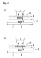
- the illumination device A of the present embodiment is described with reference to Fig. 2 .
- the blue light emitted from the light emitting element 2 transmits through the lower side transparent substrate 3 to enter the phosphor layer 4
- part of the blue light entering the phosphor layer 4 is absorbed by the phosphor 5, and then converted to the yellow light having a longer peak wavelength, or the green and red lights having longer peak wavelengths.
- the yellow light having a longer peak wavelength, or the green and red lights having longer peak wavelengths are mixed with remaining blue light in the phosphor layer 4 to form white light, which transmits through the upper side transparent substrate 3 and is emitted outside.
- Fig. 2 (a) illustrates a state where the interval between the transparent substrates 3 and 3 is expanded by the drive circuit 7, and in this case, the thickness of the phosphor layer 4 in the vertical direction (light incident direction) is increased to thereby increase the amount of the phosphor 5 positioned on a light axis of the light emitting element 2. That is, a ratio of the blue light converted in wavelength by the phosphor 5 is increased, and thereby white light close to yellow light is emitted outside.
- Fig. 2 (b) illustrates a state where the interval between the transparent substrates 3 and 3 is narrowed by the drive circuit 7, and in this case, the thickness of the phosphor layer 4 in the vertical direction is decreased to thereby decrease the amount of the phosphor 5 positioned on the light axis of the light emitting element 2. That is, the ratio of the blue light converted in wavelength by the phosphor 4a is decreased, and thereby white light close to blue light is emitted outside. Note that when the pressure applied by the drive circuit 7 is released, the state is restored by the elastic force of the binder 6.
- a region a in Figs. 2 (a) and (b) represents an emission range of the light by the light emitting element 2.
- the amount of the phosphor 5 in the same direction can be continuously changed, so that a ratio of the light converted in wavelength by the phosphor 5 can be continuously changed, and as a result, the color temperature of the incident light (light emitted from the light emitting element 2) can be continuously changed.
- the color temperature is changed, light spread in a direction orthogonal to the light incident direction can be suppressed, and as a result, the wavelength converting member 10 having a compact size can be provided.
- the thickness changing means by constituting the thickness changing means with the transparent substrates 3 and 3 and the drive circuit 7 as in the present embodiment, the thickness changing means adapted to change the thickness of the phosphor layer 4 in the light incident direction can be realized with a simple configuration. Also, by using the above-described wavelength converting member 10, the small-sized illumination device A that can continuously change the color temperature of the incident light from the light emitting element 2 can be provided.
- a second embodiment of the illumination device A according to the present invention is described below.
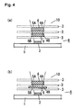
- the case where the phosphor layer is a single layer is described; however, in the present embodiment, the case where a phosphor layer includes a plurality of layers is described.
- the same components as those in the first embodiment are denoted by the same symbols, and description thereof is omitted. Also, in the following description, if it is not necessary to distinguish between phosphor layers 4A and 4B, they are collectively referred to as a phosphor layer 4.
- An illumination device A of the present invention is provided with a light emitting element 2 and a wavelength converting member 10.
- the wavelength converting member 10 is, as illustrated in Fig. 4 (a) , provided with: a plurality of (in Fig. 4 (a) , three) transparent substrates 3; and a plurality of (in Fig. 4 (a) , two) phosphor layers 4A and 4B each of which is arranged between the transparent substrates 3 and 3.
- Each of the transparent substrates 3 and 3 arranged in upper and middle stages in Fig. 4 (a) can be moved in a vertical direction by an unillustrated drive circuit to individually adjust thicknesses of the respective phosphor layers 4A and 4B in the vertical direction.
- the respective phosphor layers 4A and 4B are arranged so as to overlap with each other in the vertical direction (light incident direction).
- a green phosphor 5A is substantially uniformly dispersed
- a red phosphor 5B is substantially uniformly dispersed
- Fig. 5 is a graph illustrating a change in color temperature of the illumination device A of the present embodiment, and light transmitting through the wavelength converting part 10 shifts on a line segment e in the case of a single body of the phosphor layer 4A containing the green phosphor 5A, and in the case of a single body of the phosphor layer 4B containing the red phosphor 5B, shifts on a line segment f. Accordingly, if the thicknesses of the respective phosphor layers 4A and 4B are changed at the same rate, the light transmitting through the wavelength converting member 10 will shift on a line segment g between the line segments e and f, and in this case, change with being displaced from a blackbody locus b.
- the thickness of the one phosphor layer 4A is kept constant, and only the thickness of the other phosphor layer 4B is changed.
- the color temperature of the present illumination device A shifts on a line segment m, and therefore the color temperature change close to the blackbody locus b can be achieved.
- line segments h and k in Fig. 5 are auxiliary lines that are provided for convenience to obtain the loca of the color temperature change.
- operation of the illumination device A is the same as that in the first embodiment, and therefore description thereof is omitted here.
- the plurality of phosphor layers 4A and 4B are provided, so that as compared with the case where the phosphor layer 4 is a single layer, a color variation can be expanded, and further by individually adjusting the thicknesses of the respective phosphor layers 4A and 4B, the color temperature change close to the blackbody locus b can be achieved. Also, by using the above-described wavelength converting member 10, the small-sized illumination device A that can continuously change the color temperature of the light emitted from the light emitting element 2 can be provided.
- the illumination device A may be configured such that, as illustrated in Fig. 4 (a) , out of the plurality of phosphor layers 4A and 4B arranged so as to overlap with each other in the light incident direction, part of light emitted from the phosphor layer 4B arranged in a position close to an incident surface (lower side in Fig. 4 (a) ) is absorbed by the phosphor layer 4A arranged in a position distant from the incident surface (upper side in Fig. 4 (a) ) to emit light having a wavelength different from a wavelength of the light.
- the color temperature variation can be brought closer to the blackbody locus b.
- a locus along which the color temperature of the light is changed is different.
- the case where the number of phosphor layers 4 is two is described; however, the number of phosphor layers 4 is not limited to that in the present invention, but may be three or more.
- the case where the plurality of phosphor layers 4A and 4B are arranged so as to overlap with each other in the light incident direction is described; however, they may be arranged so as not to overlap with each other in the light incident direction (for example, a plurality of phosphor layers 4 are arranged side by side in a plane orthogonal to the light incident direction), and in this case, the color variation can be expanded in the same manner, and also if thicknesses of the respective phosphor layers 4 are individually adjusted, a color temperature change close to the blackbody locus can be achieved.
- the case where the phosphor layer 4A containing the green phosphor 5A and the phosphor layer 4B containing the red phosphor 5B are separated from each other is described; however, by changing a mixing ratio between the green phosphor 5A and the red phosphor 5B in each of the phosphor layers 4A and 4B, the plurality of phosphor layers 4A and 4B of which the mixing ratios are different may be configured.
- the thickness of the phosphor layer 4 is changed by moving the transparent substrate 3 with the drive circuit 7 ; however, there may be employed a configuration in which, for example, by applying an electric field to the phosphor layer 4, the thickness of the phosphor layer 4 is changed, and a method for changing the thickness of the phosphor layer 4 is not limited to one in any of the embodiments. Note that in the case of changing the thickness of the phosphor layer 4 by applying an electric field, it is necessary to use as the binder 6 a material of which a thickness is changed by the electric field.
Landscapes
- Physics & Mathematics (AREA)
- Spectroscopy & Molecular Physics (AREA)
- Engineering & Computer Science (AREA)
- General Engineering & Computer Science (AREA)
- Manufacturing & Machinery (AREA)
- Led Device Packages (AREA)
- Led Devices (AREA)
- Optical Filters (AREA)
Applications Claiming Priority (1)
| Application Number | Priority Date | Filing Date | Title |
|---|---|---|---|
| JP2010095242A JP2011228403A (ja) | 2010-04-16 | 2010-04-16 | 波長変換部材及びそれを用いた照明装置 |
Publications (3)
| Publication Number | Publication Date |
|---|---|
| EP2378838A2 true EP2378838A2 (de) | 2011-10-19 |
| EP2378838A3 EP2378838A3 (de) | 2012-03-07 |
| EP2378838B1 EP2378838B1 (de) | 2014-06-11 |
Family
ID=44352220
Family Applications (1)
| Application Number | Title | Priority Date | Filing Date |
|---|---|---|---|
| EP11161345.1A Not-in-force EP2378838B1 (de) | 2010-04-16 | 2011-04-06 | Wellenlängenkonvertierendes Element und Beleuchtungsvorrichtung damit |
Country Status (2)
| Country | Link |
|---|---|
| EP (1) | EP2378838B1 (de) |
| JP (1) | JP2011228403A (de) |
Cited By (2)
| Publication number | Priority date | Publication date | Assignee | Title |
|---|---|---|---|---|
| WO2018091359A1 (en) * | 2016-11-15 | 2018-05-24 | Koninklijke Philips N.V. | Light color conversion device |
| US10677437B2 (en) | 2016-09-21 | 2020-06-09 | Panasonic Intellectual Property Management Co., Ltd. | Wavelength conversion device and lighting apparatus |
Families Citing this family (3)
| Publication number | Priority date | Publication date | Assignee | Title |
|---|---|---|---|---|
| WO2013128544A1 (ja) * | 2012-02-27 | 2013-09-06 | 株式会社 セルシステム | 照明装置 |
| JP6201480B2 (ja) * | 2013-07-23 | 2017-09-27 | 日亜化学工業株式会社 | 発光装置及び照明装置 |
| JP6469893B2 (ja) * | 2016-01-26 | 2019-02-13 | シャープ株式会社 | 発光装置および照明装置 |
Citations (1)
| Publication number | Priority date | Publication date | Assignee | Title |
|---|---|---|---|---|
| JP2005347280A (ja) | 2005-07-25 | 2005-12-15 | Matsushita Electric Works Ltd | 照明器具 |
Family Cites Families (10)
| Publication number | Priority date | Publication date | Assignee | Title |
|---|---|---|---|---|
| JPH0754675B2 (ja) * | 1986-03-31 | 1995-06-07 | 株式会社東芝 | X線イメ−ジインテンシフアイア |
| US5976613A (en) * | 1993-08-03 | 1999-11-02 | Janusauskas; Albert | Method of making an electroluminescent lamp |
| US5660573A (en) * | 1994-09-08 | 1997-08-26 | Butt; James H. | Electroluminescent lamp with controlled field intensity for displaying graphics |
| JP3645422B2 (ja) * | 1998-07-14 | 2005-05-11 | 東芝電子エンジニアリング株式会社 | 発光装置 |
| JP4431241B2 (ja) * | 2000-02-18 | 2010-03-10 | スタンレー電気株式会社 | ランプ光照射装置並びに車両用前照灯 |
| US7267787B2 (en) * | 2004-08-04 | 2007-09-11 | Intematix Corporation | Phosphor systems for a white light emitting diode (LED) |
| JP4692059B2 (ja) * | 2005-04-25 | 2011-06-01 | パナソニック電工株式会社 | 発光装置の製造方法 |
| CN101401222B (zh) * | 2006-03-06 | 2010-12-01 | 皇家飞利浦电子股份有限公司 | 发光二极管模块 |
| US8783887B2 (en) * | 2007-10-01 | 2014-07-22 | Intematix Corporation | Color tunable light emitting device |
| WO2009109881A1 (en) * | 2008-03-07 | 2009-09-11 | Koninklijke Philips Electronics N.V. | Color variable light emitting device |
-
2010
- 2010-04-16 JP JP2010095242A patent/JP2011228403A/ja active Pending
-
2011
- 2011-04-06 EP EP11161345.1A patent/EP2378838B1/de not_active Not-in-force
Patent Citations (1)
| Publication number | Priority date | Publication date | Assignee | Title |
|---|---|---|---|---|
| JP2005347280A (ja) | 2005-07-25 | 2005-12-15 | Matsushita Electric Works Ltd | 照明器具 |
Cited By (3)
| Publication number | Priority date | Publication date | Assignee | Title |
|---|---|---|---|---|
| US10677437B2 (en) | 2016-09-21 | 2020-06-09 | Panasonic Intellectual Property Management Co., Ltd. | Wavelength conversion device and lighting apparatus |
| US10859249B2 (en) | 2016-09-21 | 2020-12-08 | Panasonic Intellectual Property Management Co., Ltd. | Wavelength conversion device and lighting apparatus |
| WO2018091359A1 (en) * | 2016-11-15 | 2018-05-24 | Koninklijke Philips N.V. | Light color conversion device |
Also Published As
| Publication number | Publication date |
|---|---|
| JP2011228403A (ja) | 2011-11-10 |
| EP2378838A3 (de) | 2012-03-07 |
| EP2378838B1 (de) | 2014-06-11 |
Similar Documents
| Publication | Publication Date | Title |
|---|---|---|
| US11631791B2 (en) | Semiconductor light-emitting device | |
| JP6512321B2 (ja) | 発光装置 | |
| JP6868388B2 (ja) | 発光装置および集積型発光装置 | |
| US11201269B2 (en) | Backlight including light emitting module and light reflective members | |
| US10401557B2 (en) | Semiconductor light emitting diode chip and light emitting device having the same | |
| US10763408B2 (en) | Backlight including light emitting module and light reflective members | |
| US11015784B2 (en) | Light emitting device | |
| CN113437202B (zh) | 发光装置、集成型发光装置及发光模块 | |
| JP6805532B2 (ja) | 発光装置 | |
| US11365851B2 (en) | Lighting module and lighting apparatus | |
| JP7174216B2 (ja) | 発光モジュールおよび集積型発光モジュール | |
| JP5443959B2 (ja) | 照明装置 | |
| US9761773B2 (en) | Light emitting device | |
| CN101401222B (zh) | 发光二极管模块 | |
| JP6947966B2 (ja) | 発光装置 | |
| EP2378838B1 (de) | Wellenlängenkonvertierendes Element und Beleuchtungsvorrichtung damit | |
| JP2009529232A (ja) | 発光ダイオードモジュール | |
| JP6773156B2 (ja) | 発光装置 | |
| KR20220094290A (ko) | 백색 발광장치 및 조명 장치 | |
| JP2021005569A (ja) | 発光装置 | |
| JP2020098910A (ja) | 発光装置および集積型発光装置 |
Legal Events
| Date | Code | Title | Description |
|---|---|---|---|
| AK | Designated contracting states |
Kind code of ref document: A2 Designated state(s): AL AT BE BG CH CY CZ DE DK EE ES FI FR GB GR HR HU IE IS IT LI LT LU LV MC MK MT NL NO PL PT RO RS SE SI SK SM TR |
|
| AX | Request for extension of the european patent |
Extension state: BA ME |
|
| PUAI | Public reference made under article 153(3) epc to a published international application that has entered the european phase |
Free format text: ORIGINAL CODE: 0009012 |
|
| PUAL | Search report despatched |
Free format text: ORIGINAL CODE: 0009013 |
|
| AK | Designated contracting states |
Kind code of ref document: A3 Designated state(s): AL AT BE BG CH CY CZ DE DK EE ES FI FR GB GR HR HU IE IS IT LI LT LU LV MC MK MT NL NO PL PT RO RS SE SI SK SM TR |
|
| AX | Request for extension of the european patent |
Extension state: BA ME |
|
| RIC1 | Information provided on ipc code assigned before grant |
Ipc: H05B 33/02 20060101AFI20120130BHEP Ipc: H05B 33/14 20060101ALI20120130BHEP Ipc: H05B 33/10 20060101ALI20120130BHEP |
|
| RAP1 | Party data changed (applicant data changed or rights of an application transferred) |
Owner name: PANASONIC CORPORATION |
|
| 17P | Request for examination filed |
Effective date: 20120830 |
|
| GRAJ | Information related to disapproval of communication of intention to grant by the applicant or resumption of examination proceedings by the epo deleted |
Free format text: ORIGINAL CODE: EPIDOSDIGR1 |
|
| GRAP | Despatch of communication of intention to grant a patent |
Free format text: ORIGINAL CODE: EPIDOSNIGR1 |
|
| INTG | Intention to grant announced |
Effective date: 20140109 |
|
| INTG | Intention to grant announced |
Effective date: 20140117 |
|
| GRAS | Grant fee paid |
Free format text: ORIGINAL CODE: EPIDOSNIGR3 |
|
| GRAA | (expected) grant |
Free format text: ORIGINAL CODE: 0009210 |
|
| AK | Designated contracting states |
Kind code of ref document: B1 Designated state(s): AL AT BE BG CH CY CZ DE DK EE ES FI FR GB GR HR HU IE IS IT LI LT LU LV MC MK MT NL NO PL PT RO RS SE SI SK SM TR |
|
| REG | Reference to a national code |
Ref country code: GB Ref legal event code: FG4D |
|
| REG | Reference to a national code |
Ref country code: CH Ref legal event code: EP |
|
| REG | Reference to a national code |
Ref country code: IE Ref legal event code: FG4D |
|
| REG | Reference to a national code |
Ref country code: AT Ref legal event code: REF Ref document number: 672763 Country of ref document: AT Kind code of ref document: T Effective date: 20140715 |
|
| REG | Reference to a national code |
Ref country code: DE Ref legal event code: R096 Ref document number: 602011007532 Country of ref document: DE Effective date: 20140724 |
|
| PG25 | Lapsed in a contracting state [announced via postgrant information from national office to epo] |
Ref country code: GR Free format text: LAPSE BECAUSE OF FAILURE TO SUBMIT A TRANSLATION OF THE DESCRIPTION OR TO PAY THE FEE WITHIN THE PRESCRIBED TIME-LIMIT Effective date: 20140912 Ref country code: NO Free format text: LAPSE BECAUSE OF FAILURE TO SUBMIT A TRANSLATION OF THE DESCRIPTION OR TO PAY THE FEE WITHIN THE PRESCRIBED TIME-LIMIT Effective date: 20140911 Ref country code: FI Free format text: LAPSE BECAUSE OF FAILURE TO SUBMIT A TRANSLATION OF THE DESCRIPTION OR TO PAY THE FEE WITHIN THE PRESCRIBED TIME-LIMIT Effective date: 20140611 Ref country code: LT Free format text: LAPSE BECAUSE OF FAILURE TO SUBMIT A TRANSLATION OF THE DESCRIPTION OR TO PAY THE FEE WITHIN THE PRESCRIBED TIME-LIMIT Effective date: 20140611 |
|
| REG | Reference to a national code |
Ref country code: NL Ref legal event code: VDEP Effective date: 20140611 |
|
| REG | Reference to a national code |
Ref country code: AT Ref legal event code: MK05 Ref document number: 672763 Country of ref document: AT Kind code of ref document: T Effective date: 20140611 |
|
| REG | Reference to a national code |
Ref country code: LT Ref legal event code: MG4D |
|
| PG25 | Lapsed in a contracting state [announced via postgrant information from national office to epo] |
Ref country code: HR Free format text: LAPSE BECAUSE OF FAILURE TO SUBMIT A TRANSLATION OF THE DESCRIPTION OR TO PAY THE FEE WITHIN THE PRESCRIBED TIME-LIMIT Effective date: 20140611 Ref country code: LV Free format text: LAPSE BECAUSE OF FAILURE TO SUBMIT A TRANSLATION OF THE DESCRIPTION OR TO PAY THE FEE WITHIN THE PRESCRIBED TIME-LIMIT Effective date: 20140611 Ref country code: SE Free format text: LAPSE BECAUSE OF FAILURE TO SUBMIT A TRANSLATION OF THE DESCRIPTION OR TO PAY THE FEE WITHIN THE PRESCRIBED TIME-LIMIT Effective date: 20140611 Ref country code: RS Free format text: LAPSE BECAUSE OF FAILURE TO SUBMIT A TRANSLATION OF THE DESCRIPTION OR TO PAY THE FEE WITHIN THE PRESCRIBED TIME-LIMIT Effective date: 20140611 |
|
| PG25 | Lapsed in a contracting state [announced via postgrant information from national office to epo] |
Ref country code: CZ Free format text: LAPSE BECAUSE OF FAILURE TO SUBMIT A TRANSLATION OF THE DESCRIPTION OR TO PAY THE FEE WITHIN THE PRESCRIBED TIME-LIMIT Effective date: 20140611 Ref country code: EE Free format text: LAPSE BECAUSE OF FAILURE TO SUBMIT A TRANSLATION OF THE DESCRIPTION OR TO PAY THE FEE WITHIN THE PRESCRIBED TIME-LIMIT Effective date: 20140611 Ref country code: PT Free format text: LAPSE BECAUSE OF FAILURE TO SUBMIT A TRANSLATION OF THE DESCRIPTION OR TO PAY THE FEE WITHIN THE PRESCRIBED TIME-LIMIT Effective date: 20141013 Ref country code: ES Free format text: LAPSE BECAUSE OF FAILURE TO SUBMIT A TRANSLATION OF THE DESCRIPTION OR TO PAY THE FEE WITHIN THE PRESCRIBED TIME-LIMIT Effective date: 20140611 Ref country code: RO Free format text: LAPSE BECAUSE OF FAILURE TO SUBMIT A TRANSLATION OF THE DESCRIPTION OR TO PAY THE FEE WITHIN THE PRESCRIBED TIME-LIMIT Effective date: 20140611 Ref country code: SK Free format text: LAPSE BECAUSE OF FAILURE TO SUBMIT A TRANSLATION OF THE DESCRIPTION OR TO PAY THE FEE WITHIN THE PRESCRIBED TIME-LIMIT Effective date: 20140611 |
|
| PG25 | Lapsed in a contracting state [announced via postgrant information from national office to epo] |
Ref country code: PL Free format text: LAPSE BECAUSE OF FAILURE TO SUBMIT A TRANSLATION OF THE DESCRIPTION OR TO PAY THE FEE WITHIN THE PRESCRIBED TIME-LIMIT Effective date: 20140611 Ref country code: NL Free format text: LAPSE BECAUSE OF FAILURE TO SUBMIT A TRANSLATION OF THE DESCRIPTION OR TO PAY THE FEE WITHIN THE PRESCRIBED TIME-LIMIT Effective date: 20140611 Ref country code: IS Free format text: LAPSE BECAUSE OF FAILURE TO SUBMIT A TRANSLATION OF THE DESCRIPTION OR TO PAY THE FEE WITHIN THE PRESCRIBED TIME-LIMIT Effective date: 20141011 Ref country code: AT Free format text: LAPSE BECAUSE OF FAILURE TO SUBMIT A TRANSLATION OF THE DESCRIPTION OR TO PAY THE FEE WITHIN THE PRESCRIBED TIME-LIMIT Effective date: 20140611 |
|
| REG | Reference to a national code |
Ref country code: DE Ref legal event code: R097 Ref document number: 602011007532 Country of ref document: DE |
|
| PLBE | No opposition filed within time limit |
Free format text: ORIGINAL CODE: 0009261 |
|
| STAA | Information on the status of an ep patent application or granted ep patent |
Free format text: STATUS: NO OPPOSITION FILED WITHIN TIME LIMIT |
|
| PG25 | Lapsed in a contracting state [announced via postgrant information from national office to epo] |
Ref country code: IT Free format text: LAPSE BECAUSE OF FAILURE TO SUBMIT A TRANSLATION OF THE DESCRIPTION OR TO PAY THE FEE WITHIN THE PRESCRIBED TIME-LIMIT Effective date: 20140611 Ref country code: DK Free format text: LAPSE BECAUSE OF FAILURE TO SUBMIT A TRANSLATION OF THE DESCRIPTION OR TO PAY THE FEE WITHIN THE PRESCRIBED TIME-LIMIT Effective date: 20140611 |
|
| 26N | No opposition filed |
Effective date: 20150312 |
|
| REG | Reference to a national code |
Ref country code: DE Ref legal event code: R097 Ref document number: 602011007532 Country of ref document: DE Effective date: 20150312 |
|
| PG25 | Lapsed in a contracting state [announced via postgrant information from national office to epo] |
Ref country code: BE Free format text: LAPSE BECAUSE OF FAILURE TO SUBMIT A TRANSLATION OF THE DESCRIPTION OR TO PAY THE FEE WITHIN THE PRESCRIBED TIME-LIMIT Effective date: 20140611 |
|
| PG25 | Lapsed in a contracting state [announced via postgrant information from national office to epo] |
Ref country code: SI Free format text: LAPSE BECAUSE OF FAILURE TO SUBMIT A TRANSLATION OF THE DESCRIPTION OR TO PAY THE FEE WITHIN THE PRESCRIBED TIME-LIMIT Effective date: 20140611 |
|
| PG25 | Lapsed in a contracting state [announced via postgrant information from national office to epo] |
Ref country code: MC Free format text: LAPSE BECAUSE OF FAILURE TO SUBMIT A TRANSLATION OF THE DESCRIPTION OR TO PAY THE FEE WITHIN THE PRESCRIBED TIME-LIMIT Effective date: 20140611 Ref country code: LU Free format text: LAPSE BECAUSE OF FAILURE TO SUBMIT A TRANSLATION OF THE DESCRIPTION OR TO PAY THE FEE WITHIN THE PRESCRIBED TIME-LIMIT Effective date: 20150406 |
|
| REG | Reference to a national code |
Ref country code: CH Ref legal event code: PL |
|
| GBPC | Gb: european patent ceased through non-payment of renewal fee |
Effective date: 20150406 |
|
| REG | Reference to a national code |
Ref country code: IE Ref legal event code: MM4A |
|
| PG25 | Lapsed in a contracting state [announced via postgrant information from national office to epo] |
Ref country code: CH Free format text: LAPSE BECAUSE OF NON-PAYMENT OF DUE FEES Effective date: 20150430 Ref country code: GB Free format text: LAPSE BECAUSE OF NON-PAYMENT OF DUE FEES Effective date: 20150406 Ref country code: LI Free format text: LAPSE BECAUSE OF NON-PAYMENT OF DUE FEES Effective date: 20150430 |
|
| REG | Reference to a national code |
Ref country code: FR Ref legal event code: ST Effective date: 20151231 |
|
| PG25 | Lapsed in a contracting state [announced via postgrant information from national office to epo] |
Ref country code: FR Free format text: LAPSE BECAUSE OF NON-PAYMENT OF DUE FEES Effective date: 20150430 |
|
| PG25 | Lapsed in a contracting state [announced via postgrant information from national office to epo] |
Ref country code: IE Free format text: LAPSE BECAUSE OF NON-PAYMENT OF DUE FEES Effective date: 20150406 |
|
| PG25 | Lapsed in a contracting state [announced via postgrant information from national office to epo] |
Ref country code: MT Free format text: LAPSE BECAUSE OF FAILURE TO SUBMIT A TRANSLATION OF THE DESCRIPTION OR TO PAY THE FEE WITHIN THE PRESCRIBED TIME-LIMIT Effective date: 20140611 |
|
| PG25 | Lapsed in a contracting state [announced via postgrant information from national office to epo] |
Ref country code: SM Free format text: LAPSE BECAUSE OF FAILURE TO SUBMIT A TRANSLATION OF THE DESCRIPTION OR TO PAY THE FEE WITHIN THE PRESCRIBED TIME-LIMIT Effective date: 20140611 Ref country code: BG Free format text: LAPSE BECAUSE OF FAILURE TO SUBMIT A TRANSLATION OF THE DESCRIPTION OR TO PAY THE FEE WITHIN THE PRESCRIBED TIME-LIMIT Effective date: 20140611 Ref country code: HU Free format text: LAPSE BECAUSE OF FAILURE TO SUBMIT A TRANSLATION OF THE DESCRIPTION OR TO PAY THE FEE WITHIN THE PRESCRIBED TIME-LIMIT; INVALID AB INITIO Effective date: 20110406 |
|
| PG25 | Lapsed in a contracting state [announced via postgrant information from national office to epo] |
Ref country code: CY Free format text: LAPSE BECAUSE OF FAILURE TO SUBMIT A TRANSLATION OF THE DESCRIPTION OR TO PAY THE FEE WITHIN THE PRESCRIBED TIME-LIMIT Effective date: 20140611 |
|
| PG25 | Lapsed in a contracting state [announced via postgrant information from national office to epo] |
Ref country code: TR Free format text: LAPSE BECAUSE OF FAILURE TO SUBMIT A TRANSLATION OF THE DESCRIPTION OR TO PAY THE FEE WITHIN THE PRESCRIBED TIME-LIMIT Effective date: 20140611 |
|
| PG25 | Lapsed in a contracting state [announced via postgrant information from national office to epo] |
Ref country code: MK Free format text: LAPSE BECAUSE OF FAILURE TO SUBMIT A TRANSLATION OF THE DESCRIPTION OR TO PAY THE FEE WITHIN THE PRESCRIBED TIME-LIMIT Effective date: 20140611 |
|
| PG25 | Lapsed in a contracting state [announced via postgrant information from national office to epo] |
Ref country code: AL Free format text: LAPSE BECAUSE OF FAILURE TO SUBMIT A TRANSLATION OF THE DESCRIPTION OR TO PAY THE FEE WITHIN THE PRESCRIBED TIME-LIMIT Effective date: 20140611 |
|
| PGFP | Annual fee paid to national office [announced via postgrant information from national office to epo] |
Ref country code: DE Payment date: 20190430 Year of fee payment: 9 |
|
| REG | Reference to a national code |
Ref country code: DE Ref legal event code: R119 Ref document number: 602011007532 Country of ref document: DE |
|
| PG25 | Lapsed in a contracting state [announced via postgrant information from national office to epo] |
Ref country code: DE Free format text: LAPSE BECAUSE OF NON-PAYMENT OF DUE FEES Effective date: 20201103 |