EP2378841A1 - Afficheur el organique et procédé de fabrication associé - Google Patents
Afficheur el organique et procédé de fabrication associé Download PDFInfo
- Publication number
- EP2378841A1 EP2378841A1 EP10741029A EP10741029A EP2378841A1 EP 2378841 A1 EP2378841 A1 EP 2378841A1 EP 10741029 A EP10741029 A EP 10741029A EP 10741029 A EP10741029 A EP 10741029A EP 2378841 A1 EP2378841 A1 EP 2378841A1
- Authority
- EP
- European Patent Office
- Prior art keywords
- color filter
- organic
- counter electrode
- transparent counter
- defect
- Prior art date
- Legal status (The legal status is an assumption and is not a legal conclusion. Google has not performed a legal analysis and makes no representation as to the accuracy of the status listed.)
- Granted
Links
Images





Classifications
-
- H—ELECTRICITY
- H05—ELECTRIC TECHNIQUES NOT OTHERWISE PROVIDED FOR
- H05B—ELECTRIC HEATING; ELECTRIC LIGHT SOURCES NOT OTHERWISE PROVIDED FOR; CIRCUIT ARRANGEMENTS FOR ELECTRIC LIGHT SOURCES, IN GENERAL
- H05B33/00—Electroluminescent light sources
- H05B33/10—Apparatus or processes specially adapted to the manufacture of electroluminescent light sources
-
- H—ELECTRICITY
- H05—ELECTRIC TECHNIQUES NOT OTHERWISE PROVIDED FOR
- H05B—ELECTRIC HEATING; ELECTRIC LIGHT SOURCES NOT OTHERWISE PROVIDED FOR; CIRCUIT ARRANGEMENTS FOR ELECTRIC LIGHT SOURCES, IN GENERAL
- H05B33/00—Electroluminescent light sources
- H05B33/12—Light sources with substantially two-dimensional [2D] radiating surfaces
- H05B33/26—Light sources with substantially two-dimensional [2D] radiating surfaces characterised by the composition or arrangement of the conductive material used as an electrode
-
- H—ELECTRICITY
- H05—ELECTRIC TECHNIQUES NOT OTHERWISE PROVIDED FOR
- H05B—ELECTRIC HEATING; ELECTRIC LIGHT SOURCES NOT OTHERWISE PROVIDED FOR; CIRCUIT ARRANGEMENTS FOR ELECTRIC LIGHT SOURCES, IN GENERAL
- H05B33/00—Electroluminescent light sources
- H05B33/12—Light sources with substantially two-dimensional [2D] radiating surfaces
- H05B33/26—Light sources with substantially two-dimensional [2D] radiating surfaces characterised by the composition or arrangement of the conductive material used as an electrode
- H05B33/28—Light sources with substantially two-dimensional [2D] radiating surfaces characterised by the composition or arrangement of the conductive material used as an electrode of translucent electrodes
-
- H—ELECTRICITY
- H10—SEMICONDUCTOR DEVICES; ELECTRIC SOLID-STATE DEVICES NOT OTHERWISE PROVIDED FOR
- H10K—ORGANIC ELECTRIC SOLID-STATE DEVICES
- H10K50/00—Organic light-emitting devices
- H10K50/80—Constructional details
- H10K50/805—Electrodes
- H10K50/81—Anodes
- H10K50/818—Reflective anodes, e.g. ITO combined with thick metallic layers
-
- H—ELECTRICITY
- H10—SEMICONDUCTOR DEVICES; ELECTRIC SOLID-STATE DEVICES NOT OTHERWISE PROVIDED FOR
- H10K—ORGANIC ELECTRIC SOLID-STATE DEVICES
- H10K59/00—Integrated devices, or assemblies of multiple devices, comprising at least one organic light-emitting element covered by group H10K50/00
- H10K59/10—OLED displays
- H10K59/17—Passive-matrix OLED displays
-
- H—ELECTRICITY
- H10—SEMICONDUCTOR DEVICES; ELECTRIC SOLID-STATE DEVICES NOT OTHERWISE PROVIDED FOR
- H10K—ORGANIC ELECTRIC SOLID-STATE DEVICES
- H10K59/00—Integrated devices, or assemblies of multiple devices, comprising at least one organic light-emitting element covered by group H10K50/00
- H10K59/30—Devices specially adapted for multicolour light emission
- H10K59/38—Devices specially adapted for multicolour light emission comprising colour filters or colour changing media [CCM]
-
- H—ELECTRICITY
- H10—SEMICONDUCTOR DEVICES; ELECTRIC SOLID-STATE DEVICES NOT OTHERWISE PROVIDED FOR
- H10K—ORGANIC ELECTRIC SOLID-STATE DEVICES
- H10K59/00—Integrated devices, or assemblies of multiple devices, comprising at least one organic light-emitting element covered by group H10K50/00
- H10K59/80—Constructional details
- H10K59/805—Electrodes
- H10K59/8051—Anodes
- H10K59/80518—Reflective anodes, e.g. ITO combined with thick metallic layers
-
- H—ELECTRICITY
- H10—SEMICONDUCTOR DEVICES; ELECTRIC SOLID-STATE DEVICES NOT OTHERWISE PROVIDED FOR
- H10K—ORGANIC ELECTRIC SOLID-STATE DEVICES
- H10K71/00—Manufacture or treatment specially adapted for the organic devices covered by this subclass
-
- H—ELECTRICITY
- H10—SEMICONDUCTOR DEVICES; ELECTRIC SOLID-STATE DEVICES NOT OTHERWISE PROVIDED FOR
- H10K—ORGANIC ELECTRIC SOLID-STATE DEVICES
- H10K71/00—Manufacture or treatment specially adapted for the organic devices covered by this subclass
- H10K71/70—Testing, e.g. accelerated lifetime tests
-
- H—ELECTRICITY
- H10—SEMICONDUCTOR DEVICES; ELECTRIC SOLID-STATE DEVICES NOT OTHERWISE PROVIDED FOR
- H10K—ORGANIC ELECTRIC SOLID-STATE DEVICES
- H10K2102/00—Constructional details relating to the organic devices covered by this subclass
- H10K2102/301—Details of OLEDs
- H10K2102/302—Details of OLEDs of OLED structures
- H10K2102/3023—Direction of light emission
- H10K2102/3026—Top emission
-
- H—ELECTRICITY
- H10—SEMICONDUCTOR DEVICES; ELECTRIC SOLID-STATE DEVICES NOT OTHERWISE PROVIDED FOR
- H10K—ORGANIC ELECTRIC SOLID-STATE DEVICES
- H10K50/00—Organic light-emitting devices
- H10K50/80—Constructional details
- H10K50/805—Electrodes
- H10K50/82—Cathodes
-
- H—ELECTRICITY
- H10—SEMICONDUCTOR DEVICES; ELECTRIC SOLID-STATE DEVICES NOT OTHERWISE PROVIDED FOR
- H10K—ORGANIC ELECTRIC SOLID-STATE DEVICES
- H10K50/00—Organic light-emitting devices
- H10K50/80—Constructional details
- H10K50/805—Electrodes
- H10K50/82—Cathodes
- H10K50/828—Transparent cathodes, e.g. comprising thin metal layers
-
- H—ELECTRICITY
- H10—SEMICONDUCTOR DEVICES; ELECTRIC SOLID-STATE DEVICES NOT OTHERWISE PROVIDED FOR
- H10K—ORGANIC ELECTRIC SOLID-STATE DEVICES
- H10K59/00—Integrated devices, or assemblies of multiple devices, comprising at least one organic light-emitting element covered by group H10K50/00
- H10K59/80—Constructional details
- H10K59/805—Electrodes
- H10K59/8052—Cathodes
- H10K59/80524—Transparent cathodes, e.g. comprising thin metal layers
-
- H—ELECTRICITY
- H10—SEMICONDUCTOR DEVICES; ELECTRIC SOLID-STATE DEVICES NOT OTHERWISE PROVIDED FOR
- H10K—ORGANIC ELECTRIC SOLID-STATE DEVICES
- H10K71/00—Manufacture or treatment specially adapted for the organic devices covered by this subclass
- H10K71/861—Repairing
-
- Y—GENERAL TAGGING OF NEW TECHNOLOGICAL DEVELOPMENTS; GENERAL TAGGING OF CROSS-SECTIONAL TECHNOLOGIES SPANNING OVER SEVERAL SECTIONS OF THE IPC; TECHNICAL SUBJECTS COVERED BY FORMER USPC CROSS-REFERENCE ART COLLECTIONS [XRACs] AND DIGESTS
- Y10—TECHNICAL SUBJECTS COVERED BY FORMER USPC
- Y10S—TECHNICAL SUBJECTS COVERED BY FORMER USPC CROSS-REFERENCE ART COLLECTIONS [XRACs] AND DIGESTS
- Y10S438/00—Semiconductor device manufacturing: process
- Y10S438/94—Laser ablative material removal
Definitions
- the present invention relates to an organic EL display and a manufacturing method for the same.
- organic EL displays have attracted attention as the next-generation flat display panels.
- the organic EL displays have such advantages as self-luminescence, wide viewing angle, high-contrast image, thin profile, lightweight, and low power consumption.
- Each of the organic EL devices that constitute an organic EL display generally includes a pixel electrode, a counter electrode, and an organic layer disposed between the pixel electrode and counter electrode.
- the organic layer is composed of a light-emitting layer containing fluorescent molecules, and an electron conductive thin film and a hole conductive thin film which sandwich the light-emitting layer.
- Application of voltage between the counter electrode and the pixel electrode results in the injection of electrons into the electron conductive thin film from the counter electrode and injection of holes into the hole conductive thin film from the pixel electrode, with the result that the electrons and holes are recombined in the light-emitting layer to cause luminescence.
- a manufacturing method of an organic EL display includes lamination of organic layers and thin-film electrodes, which are of the order of several tens of nanometers. This lamination process is conducted in a clean room. Nevertheless, it is not possible to completely rid the clean room of foreign material such as particles derived from an organic layer manufacturing machine or other device or from the surrounding environment. Thus, foreign material may be incorporated into the organic layer during manufacture of an organic EL display.
- the laser repair method is a process whereby current leakage via foreign material is prevented by laser irradiation of a portion of organic layer contaminated with foreign material (hereinafter also referred to as a "defect") (see, e.g., Patent Literatures 1 to 12).
- Patent Literature 1 discloses a method in which a laser beam is applied to the pixel electrode of a defective organic EL device having a color filter, so that multi-photon absorption occurs only at the pixel electrode. This allows for selective destruction (insulation) of the pixel electrode in the defect without causing destruction of other components such as a color filter, making it possible to avoid current leakage between the pixel electrode and counter electrode via the defect.
- Patent Literatures 2 to 5 disclose a method of preventing current leakage via foreign material by laser ablation of either of a pixel electrode or counter electrode at a defect.
- Patent Literature 6 discloses a method of insulating an electrode at a defect by oxidizing the electrode by laser irradiation. Insulation of the defect makes it possible to prevent current leakage via foreign material.
- Patent Literatures 7 to 9 disclose a method of preventing current leakage via foreign material by insulating the foreign material itself in the defect by laser irradiation.
- Patent Literatures 10 to 12 disclose a laser repair device having a controller and a beam generator.
- the disclosed laser repair devices are configured to identify the position of a defect present in an organic EL display panel by means of the controller and to irradiate the defect with a laser beam by means of the beam generator for insulating the defect, so that the organic EL display panel can be repaired.
- the organic EL display shows poor image quality if the difference in brightness between a defect (non-luminescent region), a dark spot, and a luminescent region is large.
- the inventor found that the brightness difference between a defect (non-luminescent region) and a luminescent region becomes large where a color filter is left directly above the defect.
- a first aspect of the present invention concerns manufacturing methods of an organic EL display given below.
- a second aspect of the present invention concerns an organic EL display given below.
- organic EL display of the present invention With the manufacturing method of organic EL display of the present invention, it is possible to prevent brightness reduction in a non-luminescent region because a portion of a color filter directly above the non-luminescent region is also ablated, thus preventing brightness variation across the organic EL display (later described).
- a manufacturing method of organic EL display of the present invention includes: 1) a first step of providing an organic EL panel; 2) a second step of detecting a defect in an organic layer of organic EL devices that constitute an organic EL panel; and 3) a third step of destroying a portion of a transparent counter electrode directly above the defect by laser irradiation through a color filter. Each step will be described in detail below.
- an organic EL panel is provided.
- the organic EL panel provided in the first step is of the top-emission type.
- the organic EL panel includes a substrate and organic EL devices disposed over the substrate in a matrix arrangement.
- Each organic EL device includes a pixel electrode disposed over the substrate, an organic layer disposed over the pixel electrode, a transparent counter electrode disposed over the organic layer, a protective layer disposed over the transparent counter electrode, and a color filter disposed over the protective layer.
- the present invention 's effects are exerted particularly when manufacturing a large-screen organic EL display; since it is likely that foreign material like particles is incorporated into the organic layer during manufacture of a large-screen organic EL display, it is highly necessary to prevent possible current leakage via the defect by means of the method of the present invention.
- the organic layer of the organic EL device may be formed either by vapor deposition or by coating method.
- the organic layers are preferably formed by the coating method.
- coating methods include inkjet printing, dispensing, nozzle coating, spin coating, intaglio printing, and relief printing.
- vapor deposition there is concern that foreign material such as particles derived from a metal mask may be incorporated in the organic layer.
- it is effective to prevent current leakage via defects by means of the method of the present invention.
- An organic EL device contained in an organic EL panel is manufactured by lamination of thin electrode films and thin organic layer films. Manufacturing of an organic EL device requires a film thickness control of the order of several tens of nanometers. Although it is typical that the manufacturing environment is well managed and manufacturing equipment is well maintained for manufacture, unwanted foreign material may be incorporated into the organic layer during manufacture (see Figs.3A and 3B ).
- the following second step and third step are directed to a method by which current leakage via a region of organic layer contaminated with such foreign material (hereinafter also referred to as a "defect") is prevented.
- organic EL devices are checked for the presence of a defect, a region of the organic layer contaminated with foreign material such as a particle (see Figs.3A and 3B ).
- defect detection method examples include visual inspection, and detection of leak light generated as a result of application of a reverse bias voltage or a forward bias voltage to the organic EL display.
- a portion of a transparent counter electrode directly above a defect which has been identified in the second step is destroyed by applying a laser beam through a color filter (hereinafter may simply referred to as "destroy a transparent counter electrode”).
- a laser beam is applied to a transparent counter electrode means to focus a laser beam onto a transparent counter electrode.
- disestroy a transparent counter electrode means to destroy the function of a transparent counter electrode, i.e., to impede current flow through the electrode.
- Figs. 1A to 1C illustrate a transparent counter electrode destroyed by laser irradiation.
- reference sign 13 represents a transparent counter electrode
- reference sign 14 represents an organic layer.
- the expression "destroy a transparent counter electrode” means to impede current flow through a laser-irradiated portion of transparent counter electrode 13 via a defect either by 1) forming space X between the laser-irradiated portion of transparent counter electrode 13 and organic layer 14 ( Fig.1A ), 2) degenerating the laser-irradiated portion of transparent counter electrode 13 to create a crack Fig.1B ), or 3 ) crashing the laser-irradiated portion of transparent counter electrode 13 ( Fig.1C ).
- a protective layer is disposed over the transparent counter electrode.
- the laser-irradiation region of the transparent counter electrode is preferably larger than the defect by 20 to 50%.
- the area of the laser-irradiation region can be adjusted by means of a slit member attached to a laser source.
- a slit member refers to a member for freely changing the laser spot size in vertical and horizontal directions. The usage of a slit member allows for defect-size dependent adjustment of the area of a laser-irradiation region.
- the laser source used for laser irradiation examples include flash lamp-pumped Nd:YAG laser.
- the wavelength of a laser beam can be selected from 1,064 nm (fundamental), 532 nm (second harmonics), 355 nm (third harmonics), and 266 nm (fourth harmonics) wavelengths.
- the wavelength of a laser beam applied to a transparent counter electrode is preferably 1,100 nm or less, most preferably 400 nm or less. That is, in the case of Nd:YAG laser, the third or fourth harmonics wavelength may be employed. This is because laser beams of 400 nm wavelength or less have less influence on the organic layer disposed below the transparent counter electrode.
- the energy (energy density) of a laser beam on the transparent counter electrode is determined depending on the material or thickness of the transparent counter electrode. For example, in the case where a transparent counter electrode (material: ITO, thickness: 100 nm) is to be destroyed with Nd:YAG laser, it is preferable to employ, when influences of laser irradiation on the color filter (later described) are not considered, the third harmonics wavelength (355 nm) while setting the energy density at 0.05 to 0.15 J/cm 2 ,.
- a portion of the transparent counter electrode directly above a defect is selectively destroyed so as to prevent current leakage via the defect, making it possible to repair an organic EL device without damaging the organic layer, TFT and other components.
- the manufacturing method of the present invention is characterized in that the method further includes a step of ablating a portion of a color filter directly above a defect in an organic layer, which defect has been detected in the second step (hereinafter may simply referred to as "ablate a color filter”).
- the step of ablating a color filter (hereinafter may simply referred to as a “filter ablation step”) may be the same step as the third step described above (see Embodiment 1) or may be a different step from the third step (see Embodiments 2 and 3).
- the filter ablation step is the same step as the third step, by laser irradiation, a color filter is ablated simultaneously with the destruction of a transparent counter electrode.
- filter ablation in the filter ablation step is accomplished by laser irradiation of a portion of the color filter directly above a defect.
- the filter ablation step may be conducted either before or after the third step, but preferably conducted before the third step.
- laser beam is applied to a color filter means to focus a laser beam on a color filter.
- ablate a color filter may mean either to completely ablate the laser-irradiated region of a color filter to form a through-hole therein (see Embodiments 1 and 2), or to partially ablate the surface of the laser-irradiated region of a color filter for thinning (see Embodiment 3).
- Thinning of a color filter may be accomplished for instance by employing a laser beam wavelength that easily passes through the color filter more easily than those used for forming a through-hole, or by reducing the energy density of laser beam to a level smaller than that of the laser beam used for forming a through-hole.
- the laser irradiation area on the color filter is preferably larger than a defect by 30 to 60%.
- the wavelength of a laser beam applied to a transparent counter electrode in the third step varies depending on whether the filter ablation step is the same step as the third step (see Embodiment 1), or the filter ablation step is a different step from the third step (see Embodiments 2 and 3).
- wavelengths of a laser beam applied to a transparent counter electrode will be described for each case.
- the laser beam applied to a transparent counter electrode preferably also has a component that does not pass through the color filter. This is because when the filter ablation step is the same step as the third step, a part of the laser beam applied to the transparent counter electrode needs to be absorbed by the color filter.
- Color filters show different light transmittance depending on their color. For example, a red color filter shows high light transmittance at 600 nm or greater; a green color filter shows high light transmittance between 480 nm and 580 nm and at 790 nm or greater; and a blue color filter shows high light transmittance between 430 nm and 500 nm and at 850 nm or greater.
- the laser beam's wavelength when the color filter directly above a defect is red, the laser beam's wavelength may be set to less than 600 nm; when the color filter directly above a defect is green, the laser beam's wavelength may be set to less than 480 nm or between greater than 580 nm and less than 790 nm; and when the color filter directly above a defect is blue, the laser beam wavelength may be set to less than 430 nm or between greater than 500 nm and less than 850 nm.
- the laser beam's wavelength further varies depending on whether (i) a color filter is present directly above a laser-irradiation region of a transparent counter electrode (see Embodiment 3), or (ii) a color filter is not present directly above a laser-irradiation region of a transparent counter electrode (see Embodiment 2).
- a color filter is present directly above a laser-irradiation region of a transparent counter electrode (case (i)).
- no color filter is present directly above a laser-irradiation region of a transparent counter electrode (case (ii)).
- the laser beam to be applied preferably has a wavelength that passes through a color filter, because the transparent counter electrode needs to be destroyed without affecting the color filter.
- the laser beam's wavelength may be set to 600 nm or greater; when the color filter directly above a defect is green, the laser beam's wavelength may be set between 480 nm and 580 nm or 790 nm or greater; and when the color filter directly above a defect is blue, the laser beam's wavelength may be set between 430 nm and 500 nm or 850 nm or greater.
- any desired wavelength can be employed because there is no need to consider influences of laser irradiation on the color filter.
- the laser beam's wavelength is preferably set to 400 nm or less - a wavelength range where a laser beam has less influence on the organic layer.
- defects can be made non-luminescent without damaging the organic layer, achieving low power consumption and high luminous efficiency. Moreover, since a color filter directly above a defect is ablated, it results in brightness elevation in the non-luminescent region. It is thus possible to reduce brightness variation across the organic EL display.
- An organic EL display of the present invention is manufactured by the above-described manufacturing method of the present invention.
- the organic EL display of the present invention is of the top-emission type, and includes a substrate and organic EL devices disposed over the substrate in a matrix arrangement.
- Each organic EL device includes a pixel electrode disposed over the substrate, an organic layer disposed over the pixel electrode, a transparent counter electrode disposed over the organic layer, a protective layer disposed over the transparent counter electrode, and a color filter disposed over the protective layer.
- sealing glass may be disposed over the color filter.
- the substrate is an insulating plate.
- the substrate may incorporate therein thin-film transistor (TFTs.)
- the pixel electrode is an electrically conductive member disposed over the substrate.
- the pixel electrode generally serves as an anode, but may serve as a cathode.
- the pixel electrode preferably has light reflectivity. Examples of materials of the pixel electrode include APC alloys (silver-palladium-copper alloys), ARA alloys (silver-ruthenium-gold alloys), MoCr alloys (molybdenum/chrome alloys), and NiCr alloys (niclcel/chrome alloys).
- the pixel electrode may be connected to the drain electrode or source electrode of a TFT through a contact hole.
- the organic layer includes an organic light-emitting layer containing organic luminescent material.
- Organic luminescent material contained in the organic light-emitting layer is preferably polymeric organic luminescent material so that the layer can be formed by coating methods.
- polymeric organic luminescent material include polyphenylenevinylene and its derivatives, polyacetylene and its derivatives, polyphenylene and its derivatives, poly para phenylene ethylene and its derivatives, poly(3-hexylthiophene) and its derivatives, and polyfluorene and its derivatives.
- the organic luminescent layer emits red, green or blue light depending on the position of the organic EL device.
- the organic layer may further include a hole injection layer, a hole transport layer, an electron transport layer, and the like.
- the transparent counter electrode is a transparent electrically conductive member disposed over the organic layer.
- the counter electrode generally serves as a cathode, but may also serve as an anode. Examples of materials of the transparent counter electrode include ITO and IZO.
- the transparent counter electrode is about 100 nm in thickness.
- the organic EL display of the present invention is characterized in that portions of the transparent counter electrode directly above defects in the organic layer are selectively destroyed.
- the protective layer is a member for protecting the organic layer against water and oxygen.
- materials of the protective layer include inorganic materials such as silicon nitrides (SiNx) and organic materials such as UV curable resins.
- the color of the color filter is appropriately determined depending on the color of light which an organic EL device emits. More specifically, an organic EL device for emitting red light includes a red color filter; an organic EL device for emitting green light includes a green color filter; and an organic EL device for emitting blue light includes a blue color filter. Examples of materials of the color filter include color resists.
- the color filter is about 1 ⁇ m in thickness.
- the organic EL display of the present invention is characterized in that a portion of a color filter directly above a defect in an organic layer is selectively ablated.
- a portion of a color filter directly above a defect is selectively ablated, so that brightness reduction at the defect (non-luminescent region) is prevented.
- the following describes how color filter ablation is correlated with prevention of brightness reduction in the non-luminescent region.
- Fig.2 illustrates organic EL device 100 having a defect, which is contained in the organic EL display of the present invention.
- organic EL device 100 a portion of the transparent counter electrode directly above a defect is destroyed, and a portion of the color filter directly above the defect is ablated.
- Organic EL device 100 includes substrate 16, pixel electrode 15, organic layer 14, transparent counter electrode 13, protective layer 12, color filter 11, and sealing glass 10.
- Foreign material 21 is incorporated into organic layer 14.
- the region of organic layer 14 contaminated with foreign material 21 constitutes defect 101.
- Arrows 50 in Fig.2 represent beams of light emitted from organic layer 14.
- defect 101 is a non-luminescent region as described above, defect 101 does not emit light as illustrated in Fig.2 .
- beams of light emitted from the surrounding region of defect 101 in organic layer 14 diffuse over defect 101.
- light can also be taken out from defect 101, a non-luminescent region.
- a portion of color filter 11 directly above defect 101 is ablated and, therefore, beams of light diffused over defect 101 do not pass through color filter 11.
- the beams of light diffused over defect 101 travel to the outside without being attenuated by color filter 11.
- color filter 11 With this configuration, even if defect 101 becomes a non-luminescent region, beams of light emitted from the surrounding region of defect 101 in organic layer 14 and diffused over defect 101 can be taken out without being attenuated, whereby brightness reduction at defect 101 can be prevented.
- Embodiment 1 describes a case where the third step and the color filter ablation step (filter ablation step) are the same step.
- Fig.3A illustrates organic EL device 100 having a defect detected in the second step (step of detecting a defect in the organic layer of an organic EL device) of the manufacturing method of the present invention.
- Organic EL device 100 of Fig.3A includes substrate 16, pixel electrode 15, organic layer 14, transparent counter electrode 13, protective layer 12, color filter 11, and sealing glass 10.
- Organic layer 14 has foreign material 21, and the region of organic layer 14 contaminated with foreign material 21 constitutes defect 101.
- the organic EL display of the present invention also includes organic EL device 103 free of any defect, such as that illustrated in Fig.3B .
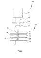
- Fig.4 illustrates a third step and a filter ablation step according to Embodiment 1.
- laser device 200 used in the third step and filter ablation step includes laser source 31, slit member 33, and focus lens 34.
- laser beam 32 is focused onto transparent counter electrode 13 through color filter 11 at a position directly above defect 101.
- the wavelength and energy density of laser beam 32 may be adjusted such that destruction of transparent counter electrode 13 and ablation of color filter 11 are effected at the same time when laser beam 32 is focused onto transparent counter electrode 13.
- the wavelength of laser beam 32 may be set to 532 nm (second harmonics) while setting the laser energy density on transparent counter electrode 13 greater than 0.7 J/cm 2 ; when color filter 11 is green, the wavelength of laser beam 32 may be set to 355 nm (third harmonics) while setting the laser energy density on transparent counter electrode 13 to 0.41 J/cm 2 or greater; and when color filter 11 is blue, the wavelength of laser beam 32 may be set to 355 nm while setting the laser energy density on transparent counter electrode 13 greater than 0.41 J/cm 2 , or the wavelength of laser beam 32 may be set to 532 nm while setting the laser energy density on transparent counter electrode 13 to 0.63 J/cm 2 or greater.
- Focusing laser beam 32 onto transparent counter electrode 12 results in the formation of through-hole 35 in color filter 11, so that destroyed portion 36 is formed in transparent counter electrode 12.
- Embodiment 1 describes a case where the third step and filter ablation step are the same step.
- Embodiment 2 describes a case where the third step and filter ablation step are different steps.
- Fig.5A illustrates a filter ablation step according to Embodiment 2.
- Fig.5B illustrates a third step according to Embodiment 2.
- laser beam 32 is first focused onto a portion of color filter 11 directly above defect 101, ablating the irradiated portion of color filter 11 to form through-hole 35.
- Laser beam 32 with a specific wavelength that cannot pass through color filter 11 is focused onto color filter 11.
- the wavelength of laser beam 32 when color filter 11 is red, the wavelength of laser beam 32 may be set to 532 nm (second harmonics) while setting the laser energy density on color filter 11 to 0.48 J/cm 2 or greater, or the wavelength of laser beam 32 may be set to 355 nm (third harmonics) while setting the laser energy density on color filter 11 to 0.32 J/cm 2 or greater; when color filter 11 is green, the wavelength of laser beam 32 may be set to 355 nm (third harmonics) while setting the laser energy density on color filter 11 to 0.32 J/cm 2 or greater; and when color filter 11 is blue, the wavelength of laser beam 32 may be set to 532 nm (second harmonics) while setting the laser energy density on color filter 11 to 0.48 J/cm 2 or greater, or the wavelength of laser beam 32 may be set to 355 nm (third harmonics) while setting the laser energy density on color filter 11 to 0.13 J/cm 2 or greater.
- laser beam 32 is focused onto a portion of transparent counter electrode 13 directly above defect 101, destroying transparent counter electrode 13 ( fig.5B ).
- the laser irradiation condition it is possible to make the laser irradiation condition more suitable for the destruction of transparent counter electrode 13 because color filter 11 has been ablated and therefore there is no need to consider influences of laser beam irradiation on color filter 11.
- the wavelength of laser beam 32 may be set to 355 nm while setting the laser energy density on transparent counter electrode 13 to 0.05 to 0.15 J/cm 2 .
- Embodiments 1 and 2 both describe a case where a laser-irradiated portion of a color filter is completely ablated to form a through-hole therein.
- Embodiment 3 describes a case where a laser-irradiated portion of a color filter is not completely ablated.
- Fig.6A illustrates a filter ablation step according to Embodiment 3.
- Fig.6B illustrates a third step according to Embodiment 3.
- laser beam 32 is first focused onto a portion of color filter 11 directly above defect 101, ablating the surface of the laser-irradiated portion of color filter 11 for thinning region 40 of color filter 11.
- This embodiment is characterized in that the wavelength or energy density of laser beam 32 is adjusted such that the laser-irradiated portion of color filter 11 is not completely ablated.
- the third step laser beam 32 is focused onto a portion of transparent counter electrode 13 directly above defect 101, destroying transparent counter electrode 13 ( Fig.6B ).
- the third step according to this embodiment is characterized in that laser beam 32 is adjusted such that color filter 11, which has been thinned in the filter ablation step, is not further ablated.
- the wavelength of laser beam 32 in the third step is adjusted such that it passes through color filter 11.
- the wavelength of laser beam 32 may be set to 1,064 nm (fundamental) while setting the laser energy density on transparent counter electrode 13 to 0.42 J/cm 2 or less.
- Embodiment 4 describes a case where material that generates fine gas bubbles by irradiation with laser beam 32 or UV light is used for a protective layer.
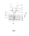
- Fig.7 illustrates a third step and a filter ablation step according to Embodiment 4.
- laser beam 32 is focused onto a portion of transparent counter electrode 103 directly above defect 101, ablating a portion of color filter directly above defect 101 and destroying the portion of transparent counter electrode 103 directly above defect 101.
- the wavelength and energy density of laser beam 32 may be adjusted such that destruction of transparent counter electrode 103 and ablation of color filter 11 are effected at the same time when laser beam 32 is focused onto transparent counter electrode 103.
- laser beam 32 passes through protective layer 12 disposed between color filter 11 and transparent counter electrode 13.
- protective layer 12 disposed between color filter 11 and transparent counter electrode 13.
- fine gas bubbles 41 are generated in protective layer 12.
- Fine gas bubbles 41 generated in protective layer 12 scatter light that are travelling around defect 101 and thereby improves brightness at defect 101.
- This embodiment describes a case where material that generates fine gas bubbles by irradiation with laser beam 32 or UV light is used for a protective layer.
- material that changes its optical refractive index by irradiation with laser beam 32 or UV light may be used for the protective layer.
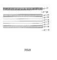
- Organic EL devices such as that illustrated in Fig.8 are provided.
- pixel electrode 15, hole injection layer 17, hole transport layer 18, organic light-emitting layer 14, electron transport layer 19, and 100 nm-thick transparent counter electrode 13 (ITO electrode) are sequentially laminated on glass substrate 16.
- glass plate 20 and a red, green or blue color filter 11 are disposed.
- three types of organic EL devices are provided, which have color filters of different colors. Examples of materials of color filter 100 include color resists. The thickness of the color filter is set to 1 ⁇ m.
- the transparent counter electrode of each of the organic EL devices provided above is irradiated with a laser beam of 1,064 nm wavelength at an energy density of 0.42 to 4.5 J/cm 2 , a laser beam of 532 nm wavelength at an energy density of 0.06 to 0.71 J/cm 2 , and a laser beam of 355 nm wavelength at an energy density of 0.05 to 0.41 J/cm 2 .
- AGT-2000RT YAG laser, manufactured by AGT Corporation
- the spot size of the laser beam on the transparent counter electrode is set to 20 ⁇ m, and pulse width is set to 3 to 5 ns. Laser irradiation is done in a single shot.
- Fig.9 is a table that lists results of laser irradiation on the color filters (CF) and transparent counter electrodes (ITO electrodes).
- Laser irradiation using 532 nm wavelength succeeds in ablating the red color filter; when the laser energy density is set to 0.56 J/cm 2 or greater, it also succeeds in ablating the blue color filter.
- the green color filter is not affected by the laser irradiation.
- laser irradiation using 532 nm fails to sufficiently destroy the ITO electrode. This is considered to be due to attenuation of the energy of the laser beam of 532 nm wavelength as a result of absorption by the red color filter.
- the color filter is red and a laser beam of 532 nm wavelength is used for destroying the ITO electrode, the laser energy density needs to be increased to greater than 0.63 J/cm 2 .
- Laser irradiation using 355 nm succeeds in ablating the blue color filter; when the laser energy density is set to 0.41 J/cm 2 or greater, it also succeeds in ablating the green color filter.
- the red color filter is not affected by the laser irradiation.
- laser irradiation using 355 nm wavelength fails to destroy the ITO electrode. This is considered to be due to attenuation of the energy of the laser beam of 355 nm wavelength as a result of absorption by the blue color filter.
- the color filter is blue and a laser beam of 355 nm wavelength is used for destroying the ITO electrode, the laser energy density needs to be increased to greater than 0.25 J/cm 2 .
- Organic EL devices such as that illustrated in Fig.8 are provided.
- pixel electrode 15, hole injection layer 17, hole transport layer 18, organic light-emitting layer 14, electron transport layer 19, and 100 nm-thick transparent counter electrode 13 (ITO electrode) are sequentially laminated on glass substrate 16.
- ITO electrode 100 nm-thick transparent counter electrode 13
- the transparent counter electrode of each of the organic EL devices provided above is irradiated with a laser beam of 1,064 nm wavelength at an energy density of 0.42 to 4.5 J/cm 2 , a laser beam of 532 nm wavelength at an energy density of 0.06 to 0.71 J/cm 2 , and a laser beam of 355 nm wavelength at an energy density of 0.05 to 0.41 J/cm 2 .
- AGT-2000RT YAG laser, manufactured by AGT Corporation
- the spot size of the laser beam on the transparent counter electrode is set to 20 ⁇ m, and pulse width is set to 3 to 5 ns. Laser irradiation is done in a single shot.
- Laser irradiations using 532 nm wavelength and 1,064 nm wavelength also damage the organic layer disposed under the transparent counter electrode (ITO electrode).
- laser irradiation using 355 nm wavelength destroys the transparent counter electrode, but does not damage the underlying organic layer. This indicates that in the case where a color filter is not present directly above the laser-irradiated portion of the transparent counter electrode, it is preferable to employ YAG laser with the third harmonics.
- the manufacturing method of the present invention With the manufacturing method of the present invention, a portion of a color filter directly above a defect is also ablated, whereby brightness reduction in the non-luminescent region (defect) can be prevented. It is thus possible to provide high-quality organic EL displays in high yields.
- the present invention can also be applied to the manufacture of other light-emitting devices having color filters.
Landscapes
- Engineering & Computer Science (AREA)
- Manufacturing & Machinery (AREA)
- Physics & Mathematics (AREA)
- Optics & Photonics (AREA)
- Electroluminescent Light Sources (AREA)
- Devices For Indicating Variable Information By Combining Individual Elements (AREA)
Applications Claiming Priority (2)
| Application Number | Priority Date | Filing Date | Title |
|---|---|---|---|
| JP2009028435 | 2009-02-10 | ||
| PCT/JP2010/000337 WO2010092749A1 (fr) | 2009-02-10 | 2010-01-21 | Afficheur el organique et procédé de fabrication associé |
Publications (3)
| Publication Number | Publication Date |
|---|---|
| EP2378841A1 true EP2378841A1 (fr) | 2011-10-19 |
| EP2378841A4 EP2378841A4 (fr) | 2012-07-18 |
| EP2378841B1 EP2378841B1 (fr) | 2013-07-31 |
Family
ID=42561598
Family Applications (1)
| Application Number | Title | Priority Date | Filing Date |
|---|---|---|---|
| EP10741029.2A Active EP2378841B1 (fr) | 2009-02-10 | 2010-01-21 | Afficheur el organique et procédé de fabrication associé |
Country Status (5)
| Country | Link |
|---|---|
| US (1) | US8772052B2 (fr) |
| EP (1) | EP2378841B1 (fr) |
| JP (1) | JP4673447B2 (fr) |
| CN (1) | CN102210193B (fr) |
| WO (1) | WO2010092749A1 (fr) |
Cited By (1)
| Publication number | Priority date | Publication date | Assignee | Title |
|---|---|---|---|---|
| CN104091901A (zh) * | 2014-06-24 | 2014-10-08 | 京东方科技集团股份有限公司 | 一种oled制备方法 |
Families Citing this family (16)
| Publication number | Priority date | Publication date | Assignee | Title |
|---|---|---|---|---|
| US8557614B2 (en) * | 2010-12-28 | 2013-10-15 | Semiconductor Energy Laboratory Co., Ltd. | Method for manufacturing lighting device |
| US8652859B2 (en) * | 2011-01-31 | 2014-02-18 | Semiconductor Energy Laboratory Co., Ltd. | Method for manufacturing light-emitting device and manufacturing apparatus of light-emitting device |
| JP5310773B2 (ja) * | 2011-04-15 | 2013-10-09 | パナソニック株式会社 | 有機elディスプレイの製造方法 |
| WO2012143974A1 (fr) * | 2011-04-20 | 2012-10-26 | パナソニック株式会社 | Procédé de fabrication d'un élément électroluminescent organique, ainsi qu'élément électroluminescent organique |
| JP5687339B2 (ja) * | 2011-06-08 | 2015-03-18 | パナソニック株式会社 | 有機el素子及び有機el素子の製造方法 |
| CN103733728B (zh) * | 2012-06-14 | 2017-03-08 | 株式会社日本有机雷特显示器 | 缺陷检测方法、有机el元件的修复方法以及有机el显示面板 |
| KR102047922B1 (ko) * | 2013-02-07 | 2019-11-25 | 삼성디스플레이 주식회사 | 플렉서블 기판, 플렉서블 기판의 제조 방법, 플렉서블 표시 장치, 및 플렉서블 표시 장치 제조 방법 |
| KR102120892B1 (ko) * | 2013-04-25 | 2020-06-10 | 삼성디스플레이 주식회사 | 박막봉지의 유기막 손상 측정방법 및 측정장치 |
| KR20150033152A (ko) * | 2013-09-23 | 2015-04-01 | 삼성디스플레이 주식회사 | 유기 발광 표시 장치의 수리 방법 |
| CN104779264A (zh) * | 2014-01-10 | 2015-07-15 | 上海和辉光电有限公司 | 混色型掩膜开口缺陷的有机发光二极管显示屏修补方法 |
| JP2017069030A (ja) * | 2015-09-30 | 2017-04-06 | 住友化学株式会社 | 有機el素子の製造方法 |
| CN107526191A (zh) * | 2016-11-09 | 2017-12-29 | 惠科股份有限公司 | 液晶面板、液晶显示器和液晶面板的修补方法 |
| JP2018170129A (ja) * | 2017-03-29 | 2018-11-01 | 株式会社ジャパンディスプレイ | 表示装置、及び表示装置の製造方法 |
| KR20220165874A (ko) | 2021-06-08 | 2022-12-16 | 삼성디스플레이 주식회사 | 표시 장치 및 그 표시 장치의 제조 방법 |
| JP2023035934A (ja) * | 2021-09-01 | 2023-03-13 | 凸版印刷株式会社 | 光学装置及びその製造方法 |
| WO2023243255A1 (fr) | 2022-06-15 | 2023-12-21 | 信越半導体株式会社 | Procédé de production d'une tranche d'éléments électroluminescents liés et procédé de transfert de micro-del |
Family Cites Families (16)
| Publication number | Priority date | Publication date | Assignee | Title |
|---|---|---|---|---|
| JP3840010B2 (ja) * | 1999-10-19 | 2006-11-01 | 東北パイオニア株式会社 | 発光ディスプレイの製造方法 |
| JP2001176672A (ja) | 1999-12-20 | 2001-06-29 | Toray Ind Inc | 有機電界発光装置およびその製造方法 |
| JP2002260857A (ja) | 2000-12-28 | 2002-09-13 | Semiconductor Energy Lab Co Ltd | 発光装置の作製方法および薄膜形成装置 |
| US6909111B2 (en) | 2000-12-28 | 2005-06-21 | Semiconductor Energy Laboratory Co., Ltd. | Method of manufacturing a light emitting device and thin film forming apparatus |
| JP2003178871A (ja) | 2001-12-11 | 2003-06-27 | Sony Corp | 有機エレクトロルミネッセンスディスプレイの製造方法及びその装置 |
| JP4270891B2 (ja) | 2003-01-21 | 2009-06-03 | 三洋電機株式会社 | El表示装置のレーザーリペア方法 |
| TWI242827B (en) | 2004-07-15 | 2005-11-01 | Ritdisplay Corp | System of detection and repair and method thereof |
| TWI237341B (en) | 2004-07-21 | 2005-08-01 | Ritdisplay Corp | System of detection and repair and method thereof |
| TWI290622B (en) | 2004-09-30 | 2007-12-01 | Ritdisplay Corp | Detection and repair system and method |
| JP2006269108A (ja) * | 2005-03-22 | 2006-10-05 | Hitachi Displays Ltd | 有機発光表示装置及びその欠陥画素の修復方法 |
| JP2006278343A (ja) | 2006-05-19 | 2006-10-12 | Tohoku Pioneer Corp | 発光ディスプレイの製造方法 |
| JP2008235178A (ja) | 2007-03-23 | 2008-10-02 | Sharp Corp | 有機elディスプレイの製造方法及び有機elディスプレイ |
| JP4924192B2 (ja) * | 2007-05-09 | 2012-04-25 | 大日本印刷株式会社 | 透明導電性膜付きカラーフィルタ基板の欠陥修正方法および透明導電性膜付きカラーフィルタ基板 |
| WO2008156284A1 (fr) * | 2007-06-18 | 2008-12-24 | Cowindst Co., Ltd. | Procédé de réparation d'un écran plat |
| JP2009016195A (ja) | 2007-07-05 | 2009-01-22 | Canon Inc | 有機発光装置のリペア方法及びそれを用いた有機発光装置の製造方法 |
| JP5104100B2 (ja) | 2007-07-30 | 2012-12-19 | マックス株式会社 | 湯水噴出装置および湯水噴出空調装置 |
-
2010
- 2010-01-21 WO PCT/JP2010/000337 patent/WO2010092749A1/fr not_active Ceased
- 2010-01-21 EP EP10741029.2A patent/EP2378841B1/fr active Active
- 2010-01-21 US US13/133,352 patent/US8772052B2/en active Active
- 2010-01-21 JP JP2010521249A patent/JP4673447B2/ja active Active
- 2010-01-21 CN CN201080003173.9A patent/CN102210193B/zh active Active
Non-Patent Citations (2)
| Title |
|---|
| No further relevant documents disclosed * |
| See also references of WO2010092749A1 * |
Cited By (1)
| Publication number | Priority date | Publication date | Assignee | Title |
|---|---|---|---|---|
| CN104091901A (zh) * | 2014-06-24 | 2014-10-08 | 京东方科技集团股份有限公司 | 一种oled制备方法 |
Also Published As
| Publication number | Publication date |
|---|---|
| CN102210193B (zh) | 2014-12-10 |
| WO2010092749A1 (fr) | 2010-08-19 |
| JP4673447B2 (ja) | 2011-04-20 |
| US20110278603A1 (en) | 2011-11-17 |
| CN102210193A (zh) | 2011-10-05 |
| US8772052B2 (en) | 2014-07-08 |
| EP2378841B1 (fr) | 2013-07-31 |
| EP2378841A4 (fr) | 2012-07-18 |
| JPWO2010092749A1 (ja) | 2012-08-16 |
Similar Documents
| Publication | Publication Date | Title |
|---|---|---|
| EP2378841B1 (fr) | Afficheur el organique et procédé de fabrication associé | |
| EP2424334B1 (fr) | Procédé de fabrication d'un dispositif d'affichage électroluminescent organique | |
| JP5310773B2 (ja) | 有機elディスプレイの製造方法 | |
| US7964416B2 (en) | Manufacturing method of organic EL display | |
| US7332263B2 (en) | Method for patterning an organic light emitting diode device | |
| JP2008235178A (ja) | 有機elディスプレイの製造方法及び有機elディスプレイ | |
| JP2008235177A (ja) | 有機elディスプレイの製造方法及び有機elディスプレイ | |
| US8062085B2 (en) | Method of producing organic light emitting device | |
| JP5351297B2 (ja) | 有機el素子の製造方法 | |
| GB2494957A (en) | Repairing short circuit manufacturing defects in OLED displays | |
| JP2001176672A (ja) | 有機電界発光装置およびその製造方法 | |
| US20110186819A1 (en) | Organic electroluminescence display apparatus and manufacturing method therefor | |
| JP2008268880A (ja) | 有機発光装置の製造方法 | |
| JP2011113733A (ja) | 有機elディスプレイの製造方法 | |
| KR101848502B1 (ko) | 유기전계발광표시장치의 리페어방법 | |
| JP2010267420A (ja) | 有機el素子検査リペア方法および装置 | |
| JP2012204105A (ja) | 表示基板の欠陥修正方法 | |
| JP2009301934A (ja) | 有機el表示装置の製造方法 | |
| JP2011228227A (ja) | 有機elディスプレイの製造方法、及び有機elディスプレイ |
Legal Events
| Date | Code | Title | Description |
|---|---|---|---|
| PUAI | Public reference made under article 153(3) epc to a published international application that has entered the european phase |
Free format text: ORIGINAL CODE: 0009012 |
|
| 17P | Request for examination filed |
Effective date: 20110524 |
|
| AK | Designated contracting states |
Kind code of ref document: A1 Designated state(s): AT BE BG CH CY CZ DE DK EE ES FI FR GB GR HR HU IE IS IT LI LT LU LV MC MK MT NL NO PL PT RO SE SI SK SM TR |
|
| DAX | Request for extension of the european patent (deleted) | ||
| A4 | Supplementary search report drawn up and despatched |
Effective date: 20120614 |
|
| RIC1 | Information provided on ipc code assigned before grant |
Ipc: H05B 33/10 20060101ALI20120608BHEP Ipc: H05B 33/28 20060101ALI20120608BHEP Ipc: H01L 51/52 20060101ALI20120608BHEP Ipc: H05B 33/12 20060101ALI20120608BHEP Ipc: H01L 51/56 20060101ALI20120608BHEP Ipc: H01L 27/32 20060101AFI20120608BHEP Ipc: H05B 33/26 20060101ALI20120608BHEP Ipc: G09F 9/00 20060101ALI20120608BHEP |
|
| REG | Reference to a national code |
Ref country code: DE Ref legal event code: R079 Ref document number: 602010009086 Country of ref document: DE Free format text: PREVIOUS MAIN CLASS: H05B0033100000 Ipc: H01L0027320000 |
|
| RIC1 | Information provided on ipc code assigned before grant |
Ipc: H05B 33/28 20060101ALI20130109BHEP Ipc: H01L 27/32 20060101AFI20130109BHEP Ipc: H01L 51/52 20060101ALI20130109BHEP Ipc: H01L 51/56 20060101ALI20130109BHEP Ipc: H05B 33/26 20060101ALI20130109BHEP Ipc: H05B 33/10 20060101ALI20130109BHEP |
|
| GRAP | Despatch of communication of intention to grant a patent |
Free format text: ORIGINAL CODE: EPIDOSNIGR1 |
|
| GRAS | Grant fee paid |
Free format text: ORIGINAL CODE: EPIDOSNIGR3 |
|
| GRAA | (expected) grant |
Free format text: ORIGINAL CODE: 0009210 |
|
| AK | Designated contracting states |
Kind code of ref document: B1 Designated state(s): AT BE BG CH CY CZ DE DK EE ES FI FR GB GR HR HU IE IS IT LI LT LU LV MC MK MT NL NO PL PT RO SE SI SK SM TR |
|
| REG | Reference to a national code |
Ref country code: GB Ref legal event code: FG4D Ref country code: CH Ref legal event code: EP |
|
| REG | Reference to a national code |
Ref country code: AT Ref legal event code: REF Ref document number: 625080 Country of ref document: AT Kind code of ref document: T Effective date: 20130815 |
|
| REG | Reference to a national code |
Ref country code: IE Ref legal event code: FG4D |
|
| REG | Reference to a national code |
Ref country code: DE Ref legal event code: R096 Ref document number: 602010009086 Country of ref document: DE Effective date: 20130926 |
|
| REG | Reference to a national code |
Ref country code: AT Ref legal event code: MK05 Ref document number: 625080 Country of ref document: AT Kind code of ref document: T Effective date: 20130731 |
|
| REG | Reference to a national code |
Ref country code: NL Ref legal event code: VDEP Effective date: 20130731 |
|
| REG | Reference to a national code |
Ref country code: LT Ref legal event code: MG4D |
|
| PG25 | Lapsed in a contracting state [announced via postgrant information from national office to epo] |
Ref country code: PT Free format text: LAPSE BECAUSE OF FAILURE TO SUBMIT A TRANSLATION OF THE DESCRIPTION OR TO PAY THE FEE WITHIN THE PRESCRIBED TIME-LIMIT Effective date: 20131202 Ref country code: BE Free format text: LAPSE BECAUSE OF FAILURE TO SUBMIT A TRANSLATION OF THE DESCRIPTION OR TO PAY THE FEE WITHIN THE PRESCRIBED TIME-LIMIT Effective date: 20130731 Ref country code: LT Free format text: LAPSE BECAUSE OF FAILURE TO SUBMIT A TRANSLATION OF THE DESCRIPTION OR TO PAY THE FEE WITHIN THE PRESCRIBED TIME-LIMIT Effective date: 20130731 Ref country code: IS Free format text: LAPSE BECAUSE OF FAILURE TO SUBMIT A TRANSLATION OF THE DESCRIPTION OR TO PAY THE FEE WITHIN THE PRESCRIBED TIME-LIMIT Effective date: 20131130 Ref country code: NO Free format text: LAPSE BECAUSE OF FAILURE TO SUBMIT A TRANSLATION OF THE DESCRIPTION OR TO PAY THE FEE WITHIN THE PRESCRIBED TIME-LIMIT Effective date: 20131031 Ref country code: SE Free format text: LAPSE BECAUSE OF FAILURE TO SUBMIT A TRANSLATION OF THE DESCRIPTION OR TO PAY THE FEE WITHIN THE PRESCRIBED TIME-LIMIT Effective date: 20130731 Ref country code: CY Free format text: LAPSE BECAUSE OF FAILURE TO SUBMIT A TRANSLATION OF THE DESCRIPTION OR TO PAY THE FEE WITHIN THE PRESCRIBED TIME-LIMIT Effective date: 20130724 Ref country code: HR Free format text: LAPSE BECAUSE OF FAILURE TO SUBMIT A TRANSLATION OF THE DESCRIPTION OR TO PAY THE FEE WITHIN THE PRESCRIBED TIME-LIMIT Effective date: 20130731 Ref country code: AT Free format text: LAPSE BECAUSE OF FAILURE TO SUBMIT A TRANSLATION OF THE DESCRIPTION OR TO PAY THE FEE WITHIN THE PRESCRIBED TIME-LIMIT Effective date: 20130731 |
|
| PG25 | Lapsed in a contracting state [announced via postgrant information from national office to epo] |
Ref country code: NL Free format text: LAPSE BECAUSE OF FAILURE TO SUBMIT A TRANSLATION OF THE DESCRIPTION OR TO PAY THE FEE WITHIN THE PRESCRIBED TIME-LIMIT Effective date: 20130731 Ref country code: SI Free format text: LAPSE BECAUSE OF FAILURE TO SUBMIT A TRANSLATION OF THE DESCRIPTION OR TO PAY THE FEE WITHIN THE PRESCRIBED TIME-LIMIT Effective date: 20130731 Ref country code: PL Free format text: LAPSE BECAUSE OF FAILURE TO SUBMIT A TRANSLATION OF THE DESCRIPTION OR TO PAY THE FEE WITHIN THE PRESCRIBED TIME-LIMIT Effective date: 20130731 Ref country code: GR Free format text: LAPSE BECAUSE OF FAILURE TO SUBMIT A TRANSLATION OF THE DESCRIPTION OR TO PAY THE FEE WITHIN THE PRESCRIBED TIME-LIMIT Effective date: 20131101 Ref country code: FI Free format text: LAPSE BECAUSE OF FAILURE TO SUBMIT A TRANSLATION OF THE DESCRIPTION OR TO PAY THE FEE WITHIN THE PRESCRIBED TIME-LIMIT Effective date: 20130731 Ref country code: LV Free format text: LAPSE BECAUSE OF FAILURE TO SUBMIT A TRANSLATION OF THE DESCRIPTION OR TO PAY THE FEE WITHIN THE PRESCRIBED TIME-LIMIT Effective date: 20130731 |
|
| PG25 | Lapsed in a contracting state [announced via postgrant information from national office to epo] |
Ref country code: CY Free format text: LAPSE BECAUSE OF FAILURE TO SUBMIT A TRANSLATION OF THE DESCRIPTION OR TO PAY THE FEE WITHIN THE PRESCRIBED TIME-LIMIT Effective date: 20130731 |
|
| PG25 | Lapsed in a contracting state [announced via postgrant information from national office to epo] |
Ref country code: RO Free format text: LAPSE BECAUSE OF FAILURE TO SUBMIT A TRANSLATION OF THE DESCRIPTION OR TO PAY THE FEE WITHIN THE PRESCRIBED TIME-LIMIT Effective date: 20130731 Ref country code: DK Free format text: LAPSE BECAUSE OF FAILURE TO SUBMIT A TRANSLATION OF THE DESCRIPTION OR TO PAY THE FEE WITHIN THE PRESCRIBED TIME-LIMIT Effective date: 20130731 Ref country code: EE Free format text: LAPSE BECAUSE OF FAILURE TO SUBMIT A TRANSLATION OF THE DESCRIPTION OR TO PAY THE FEE WITHIN THE PRESCRIBED TIME-LIMIT Effective date: 20130731 Ref country code: SK Free format text: LAPSE BECAUSE OF FAILURE TO SUBMIT A TRANSLATION OF THE DESCRIPTION OR TO PAY THE FEE WITHIN THE PRESCRIBED TIME-LIMIT Effective date: 20130731 Ref country code: CZ Free format text: LAPSE BECAUSE OF FAILURE TO SUBMIT A TRANSLATION OF THE DESCRIPTION OR TO PAY THE FEE WITHIN THE PRESCRIBED TIME-LIMIT Effective date: 20130731 |
|
| PG25 | Lapsed in a contracting state [announced via postgrant information from national office to epo] |
Ref country code: IT Free format text: LAPSE BECAUSE OF FAILURE TO SUBMIT A TRANSLATION OF THE DESCRIPTION OR TO PAY THE FEE WITHIN THE PRESCRIBED TIME-LIMIT Effective date: 20130731 Ref country code: ES Free format text: LAPSE BECAUSE OF FAILURE TO SUBMIT A TRANSLATION OF THE DESCRIPTION OR TO PAY THE FEE WITHIN THE PRESCRIBED TIME-LIMIT Effective date: 20130731 |
|
| PLBE | No opposition filed within time limit |
Free format text: ORIGINAL CODE: 0009261 |
|
| STAA | Information on the status of an ep patent application or granted ep patent |
Free format text: STATUS: NO OPPOSITION FILED WITHIN TIME LIMIT |
|
| 26N | No opposition filed |
Effective date: 20140502 |
|
| REG | Reference to a national code |
Ref country code: DE Ref legal event code: R097 Ref document number: 602010009086 Country of ref document: DE Effective date: 20140502 |
|
| PG25 | Lapsed in a contracting state [announced via postgrant information from national office to epo] |
Ref country code: LU Free format text: LAPSE BECAUSE OF FAILURE TO SUBMIT A TRANSLATION OF THE DESCRIPTION OR TO PAY THE FEE WITHIN THE PRESCRIBED TIME-LIMIT Effective date: 20140121 |
|
| REG | Reference to a national code |
Ref country code: CH Ref legal event code: PL |
|
| GBPC | Gb: european patent ceased through non-payment of renewal fee |
Effective date: 20140121 |
|
| PG25 | Lapsed in a contracting state [announced via postgrant information from national office to epo] |
Ref country code: CH Free format text: LAPSE BECAUSE OF NON-PAYMENT OF DUE FEES Effective date: 20140131 Ref country code: LI Free format text: LAPSE BECAUSE OF NON-PAYMENT OF DUE FEES Effective date: 20140131 |
|
| REG | Reference to a national code |
Ref country code: FR Ref legal event code: ST Effective date: 20140930 |
|
| REG | Reference to a national code |
Ref country code: IE Ref legal event code: MM4A |
|
| PG25 | Lapsed in a contracting state [announced via postgrant information from national office to epo] |
Ref country code: GB Free format text: LAPSE BECAUSE OF NON-PAYMENT OF DUE FEES Effective date: 20140121 Ref country code: FR Free format text: LAPSE BECAUSE OF NON-PAYMENT OF DUE FEES Effective date: 20140131 |
|
| PG25 | Lapsed in a contracting state [announced via postgrant information from national office to epo] |
Ref country code: IE Free format text: LAPSE BECAUSE OF NON-PAYMENT OF DUE FEES Effective date: 20140121 |
|
| PG25 | Lapsed in a contracting state [announced via postgrant information from national office to epo] |
Ref country code: MC Free format text: LAPSE BECAUSE OF FAILURE TO SUBMIT A TRANSLATION OF THE DESCRIPTION OR TO PAY THE FEE WITHIN THE PRESCRIBED TIME-LIMIT Effective date: 20130731 |
|
| REG | Reference to a national code |
Ref country code: DE Ref legal event code: R082 Ref document number: 602010009086 Country of ref document: DE Representative=s name: SCHWABE SANDMAIR MARX, DE Ref country code: DE Ref legal event code: R081 Ref document number: 602010009086 Country of ref document: DE Owner name: JOLED INC., TOKYO, JP Free format text: FORMER OWNER: PANASONIC CORPORATION, KADOMA-SHI, OSAKA, JP Ref country code: DE Ref legal event code: R082 Ref document number: 602010009086 Country of ref document: DE Representative=s name: SCHWABE SANDMAIR MARX PATENTANWAELTE RECHTSANW, DE |
|
| PG25 | Lapsed in a contracting state [announced via postgrant information from national office to epo] |
Ref country code: MT Free format text: LAPSE BECAUSE OF FAILURE TO SUBMIT A TRANSLATION OF THE DESCRIPTION OR TO PAY THE FEE WITHIN THE PRESCRIBED TIME-LIMIT Effective date: 20130731 |
|
| PG25 | Lapsed in a contracting state [announced via postgrant information from national office to epo] |
Ref country code: SM Free format text: LAPSE BECAUSE OF FAILURE TO SUBMIT A TRANSLATION OF THE DESCRIPTION OR TO PAY THE FEE WITHIN THE PRESCRIBED TIME-LIMIT Effective date: 20130731 |
|
| PG25 | Lapsed in a contracting state [announced via postgrant information from national office to epo] |
Ref country code: BG Free format text: LAPSE BECAUSE OF FAILURE TO SUBMIT A TRANSLATION OF THE DESCRIPTION OR TO PAY THE FEE WITHIN THE PRESCRIBED TIME-LIMIT Effective date: 20130731 |
|
| PG25 | Lapsed in a contracting state [announced via postgrant information from national office to epo] |
Ref country code: TR Free format text: LAPSE BECAUSE OF FAILURE TO SUBMIT A TRANSLATION OF THE DESCRIPTION OR TO PAY THE FEE WITHIN THE PRESCRIBED TIME-LIMIT Effective date: 20130731 Ref country code: HU Free format text: LAPSE BECAUSE OF FAILURE TO SUBMIT A TRANSLATION OF THE DESCRIPTION OR TO PAY THE FEE WITHIN THE PRESCRIBED TIME-LIMIT; INVALID AB INITIO Effective date: 20100121 |
|
| PG25 | Lapsed in a contracting state [announced via postgrant information from national office to epo] |
Ref country code: MK Free format text: LAPSE BECAUSE OF FAILURE TO SUBMIT A TRANSLATION OF THE DESCRIPTION OR TO PAY THE FEE WITHIN THE PRESCRIBED TIME-LIMIT Effective date: 20130731 |
|
| REG | Reference to a national code |
Ref country code: DE Ref legal event code: R079 Ref document number: 602010009086 Country of ref document: DE Free format text: PREVIOUS MAIN CLASS: H01L0027320000 Ipc: H10K0059000000 |
|
| REG | Reference to a national code |
Ref country code: DE Ref legal event code: R082 Ref document number: 602010009086 Country of ref document: DE Representative=s name: DENNEMEYER & ASSOCIATES S.A., DE Ref country code: DE Ref legal event code: R082 Ref document number: 602010009086 Country of ref document: DE Representative=s name: DENNEMEYER & ASSOCIATES RECHTSANWALTSGESELLSCH, DE Ref country code: DE Ref legal event code: R081 Ref document number: 602010009086 Country of ref document: DE Owner name: JDI DESIGN AND DEVELOPMENT G.K., JP Free format text: FORMER OWNER: JOLED INC., TOKYO, CHIYODA-KU, JP Ref country code: DE Ref legal event code: R081 Ref document number: 602010009086 Country of ref document: DE Owner name: MAGNOLIA BLUE CORPORATION, JP Free format text: FORMER OWNER: JOLED INC., TOKYO, CHIYODA-KU, JP Ref country code: DE Ref legal event code: R082 Ref document number: 602010009086 Country of ref document: DE Representative=s name: MERH-IP MATIAS ERNY REICHL HOFFMANN PATENTANWA, DE |
|
| REG | Reference to a national code |
Ref country code: DE Ref legal event code: R082 Ref document number: 602010009086 Country of ref document: DE Representative=s name: DENNEMEYER & ASSOCIATES RECHTSANWALTSGESELLSCH, DE Ref country code: DE Ref legal event code: R082 Ref document number: 602010009086 Country of ref document: DE Representative=s name: MERH-IP MATIAS ERNY REICHL HOFFMANN PATENTANWA, DE |
|
| REG | Reference to a national code |
Ref country code: DE Ref legal event code: R081 Ref document number: 602010009086 Country of ref document: DE Owner name: MAGNOLIA BLUE CORPORATION, JP Free format text: FORMER OWNER: JDI DESIGN AND DEVELOPMENT G.K., TOKYO, JP Ref country code: DE Ref legal event code: R082 Ref document number: 602010009086 Country of ref document: DE Representative=s name: MERH-IP MATIAS ERNY REICHL HOFFMANN PATENTANWA, DE |
|
| PGFP | Annual fee paid to national office [announced via postgrant information from national office to epo] |
Ref country code: DE Payment date: 20260121 Year of fee payment: 17 |