EP2380038B1 - Cmos bildaufnehmer - Google Patents
Cmos bildaufnehmer Download PDFInfo
- Publication number
- EP2380038B1 EP2380038B1 EP09774935.2A EP09774935A EP2380038B1 EP 2380038 B1 EP2380038 B1 EP 2380038B1 EP 09774935 A EP09774935 A EP 09774935A EP 2380038 B1 EP2380038 B1 EP 2380038B1
- Authority
- EP
- European Patent Office
- Prior art keywords
- image
- color
- photodetectors
- intensity
- apd
- Prior art date
- Legal status (The legal status is an assumption and is not a legal conclusion. Google has not performed a legal analysis and makes no representation as to the accuracy of the status listed.)
- Not-in-force
Links
- 238000003384 imaging method Methods 0.000 claims description 71
- 238000003491 array Methods 0.000 claims description 13
- 238000012545 processing Methods 0.000 claims description 12
- 230000004297 night vision Effects 0.000 claims description 10
- 230000004913 activation Effects 0.000 claims description 7
- 230000008878 coupling Effects 0.000 claims description 2
- 238000010168 coupling process Methods 0.000 claims description 2
- 238000005859 coupling reaction Methods 0.000 claims description 2
- 238000002059 diagnostic imaging Methods 0.000 claims description 2
- 238000013459 approach Methods 0.000 description 11
- 230000003287 optical effect Effects 0.000 description 9
- 230000035945 sensitivity Effects 0.000 description 8
- 230000008901 benefit Effects 0.000 description 7
- 230000004048 modification Effects 0.000 description 6
- 238000012986 modification Methods 0.000 description 6
- 238000000034 method Methods 0.000 description 5
- 230000003321 amplification Effects 0.000 description 4
- 238000001514 detection method Methods 0.000 description 4
- 238000003199 nucleic acid amplification method Methods 0.000 description 4
- FYLGZBNNVGZPIW-UHFFFAOYSA-N 1-[4-(1,4-dioxa-8-azaspiro[4.5]decan-8-yl)phenyl]ethanone Chemical compound C1=CC(C(=O)C)=CC=C1N1CCC2(OCCO2)CC1 FYLGZBNNVGZPIW-UHFFFAOYSA-N 0.000 description 3
- 206010034960 Photophobia Diseases 0.000 description 3
- 208000013469 light sensitivity Diseases 0.000 description 3
- 238000004519 manufacturing process Methods 0.000 description 3
- 238000001429 visible spectrum Methods 0.000 description 3
- 230000004075 alteration Effects 0.000 description 2
- 230000015556 catabolic process Effects 0.000 description 2
- 239000003086 colorant Substances 0.000 description 2
- 230000004069 differentiation Effects 0.000 description 2
- 230000008569 process Effects 0.000 description 2
- 238000011002 quantification Methods 0.000 description 2
- 230000009467 reduction Effects 0.000 description 2
- 239000004065 semiconductor Substances 0.000 description 2
- XUIMIQQOPSSXEZ-UHFFFAOYSA-N Silicon Chemical compound [Si] XUIMIQQOPSSXEZ-UHFFFAOYSA-N 0.000 description 1
- 238000010521 absorption reaction Methods 0.000 description 1
- 230000002411 adverse Effects 0.000 description 1
- 239000000872 buffer Substances 0.000 description 1
- 239000000969 carrier Substances 0.000 description 1
- 238000004891 communication Methods 0.000 description 1
- 230000001419 dependent effect Effects 0.000 description 1
- 238000013461 design Methods 0.000 description 1
- 238000010586 diagram Methods 0.000 description 1
- 230000005684 electric field Effects 0.000 description 1
- 238000001914 filtration Methods 0.000 description 1
- 230000004907 flux Effects 0.000 description 1
- 230000006870 function Effects 0.000 description 1
- 239000011521 glass Substances 0.000 description 1
- 238000005286 illumination Methods 0.000 description 1
- 230000006872 improvement Effects 0.000 description 1
- 238000003780 insertion Methods 0.000 description 1
- 230000037431 insertion Effects 0.000 description 1
- 230000010354 integration Effects 0.000 description 1
- 230000004807 localization Effects 0.000 description 1
- 239000011159 matrix material Substances 0.000 description 1
- 238000005259 measurement Methods 0.000 description 1
- 230000037361 pathway Effects 0.000 description 1
- 230000011514 reflex Effects 0.000 description 1
- 230000004044 response Effects 0.000 description 1
- 229920006395 saturated elastomer Polymers 0.000 description 1
- 229910052710 silicon Inorganic materials 0.000 description 1
- 239000010703 silicon Substances 0.000 description 1
- 239000002210 silicon-based material Substances 0.000 description 1
- 230000003595 spectral effect Effects 0.000 description 1
- 239000000758 substrate Substances 0.000 description 1
- 230000002123 temporal effect Effects 0.000 description 1
- 239000012780 transparent material Substances 0.000 description 1
- 230000001960 triggered effect Effects 0.000 description 1
Images




Classifications
-
- G—PHYSICS
- G01—MEASURING; TESTING
- G01S—RADIO DIRECTION-FINDING; RADIO NAVIGATION; DETERMINING DISTANCE OR VELOCITY BY USE OF RADIO WAVES; LOCATING OR PRESENCE-DETECTING BY USE OF THE REFLECTION OR RERADIATION OF RADIO WAVES; ANALOGOUS ARRANGEMENTS USING OTHER WAVES
- G01S17/00—Systems using the reflection or reradiation of electromagnetic waves other than radio waves, e.g. lidar systems
- G01S17/02—Systems using the reflection of electromagnetic waves other than radio waves
- G01S17/06—Systems determining position data of a target
- G01S17/08—Systems determining position data of a target for measuring distance only
- G01S17/10—Systems determining position data of a target for measuring distance only using transmission of interrupted, pulse-modulated waves
-
- G—PHYSICS
- G01—MEASURING; TESTING
- G01S—RADIO DIRECTION-FINDING; RADIO NAVIGATION; DETERMINING DISTANCE OR VELOCITY BY USE OF RADIO WAVES; LOCATING OR PRESENCE-DETECTING BY USE OF THE REFLECTION OR RERADIATION OF RADIO WAVES; ANALOGOUS ARRANGEMENTS USING OTHER WAVES
- G01S17/00—Systems using the reflection or reradiation of electromagnetic waves other than radio waves, e.g. lidar systems
- G01S17/86—Combinations of lidar systems with systems other than lidar, radar or sonar, e.g. with direction finders
-
- G—PHYSICS
- G01—MEASURING; TESTING
- G01S—RADIO DIRECTION-FINDING; RADIO NAVIGATION; DETERMINING DISTANCE OR VELOCITY BY USE OF RADIO WAVES; LOCATING OR PRESENCE-DETECTING BY USE OF THE REFLECTION OR RERADIATION OF RADIO WAVES; ANALOGOUS ARRANGEMENTS USING OTHER WAVES
- G01S17/00—Systems using the reflection or reradiation of electromagnetic waves other than radio waves, e.g. lidar systems
- G01S17/88—Lidar systems specially adapted for specific applications
- G01S17/89—Lidar systems specially adapted for specific applications for mapping or imaging
-
- H—ELECTRICITY
- H04—ELECTRIC COMMUNICATION TECHNIQUE
- H04N—PICTORIAL COMMUNICATION, e.g. TELEVISION
- H04N23/00—Cameras or camera modules comprising electronic image sensors; Control thereof
- H04N23/80—Camera processing pipelines; Components thereof
- H04N23/84—Camera processing pipelines; Components thereof for processing colour signals
-
- H—ELECTRICITY
- H04—ELECTRIC COMMUNICATION TECHNIQUE
- H04N—PICTORIAL COMMUNICATION, e.g. TELEVISION
- H04N25/00—Circuitry of solid-state image sensors [SSIS]; Control thereof
- H04N25/70—SSIS architectures; Circuits associated therewith
- H04N25/76—Addressed sensors, e.g. MOS or CMOS sensors
- H04N25/77—Pixel circuitry, e.g. memories, A/D converters, pixel amplifiers, shared circuits or shared components
- H04N25/772—Pixel circuitry, e.g. memories, A/D converters, pixel amplifiers, shared circuits or shared components comprising A/D, V/T, V/F, I/T or I/F converters
- H04N25/773—Pixel circuitry, e.g. memories, A/D converters, pixel amplifiers, shared circuits or shared components comprising A/D, V/T, V/F, I/T or I/F converters comprising photon counting circuits, e.g. single photon detection [SPD] or single photon avalanche diodes [SPAD]
-
- H—ELECTRICITY
- H04—ELECTRIC COMMUNICATION TECHNIQUE
- H04N—PICTORIAL COMMUNICATION, e.g. TELEVISION
- H04N25/00—Circuitry of solid-state image sensors [SSIS]; Control thereof
- H04N25/10—Circuitry of solid-state image sensors [SSIS]; Control thereof for transforming different wavelengths into image signals
- H04N25/11—Arrangement of colour filter arrays [CFA]; Filter mosaics
- H04N25/13—Arrangement of colour filter arrays [CFA]; Filter mosaics characterised by the spectral characteristics of the filter elements
- H04N25/134—Arrangement of colour filter arrays [CFA]; Filter mosaics characterised by the spectral characteristics of the filter elements based on three different wavelength filter elements
Definitions
- the following relates to the imaging arts, photographic arts, audio/video arts, remote communication arts, and related arts.
- Digital imaging is used in diverse applications such as digital cameras, web cameras (“webcams”), audio/video cameras (“camcorders”), and so forth.
- a CMOS imager is employed, in which an array of broadband photodetectors are coupled with color-selective filters to define color-selective photodetectors.
- CMOS color imaging arrays sometimes employ a Bayer pattern that includes 50% green photodetectors, 25% blue photodetectors, and 25% red photodetectors.
- the color-selective photodetectors are biased through a reset transistor, and impingement of light generates a detectable voltage reduction.
- the voltage can be amplified by suitable amplification circuitry.
- CMOS imagers have poor sensitivity to low light conditions, even when operated in conjunction with signal amplification circuitry.
- One source of light intensity loss is the color-selective filters. For a given light intensity, each color-selective filter typically removes about two-thirds of the light (corresponding to the non-selected colors), although the filtering loss is dependent upon the type of filter used.
- panchromatic photodetectors are similar to the color-selective photodetectors, but do not have color-selective filters.
- the panchromatic photodetectors generate a luminance image, which is an image of light intensity substantially independent of light color or wavelength, as acquired by broadband or panchromatic photodetectors.
- Digital image processing circuitry combines the color image generated by the color-selective photodetectors and the luminance image generated by the broadband or panchromatic photodetectors to generate an output image.
- Some systems employing such interspersed color-selective and panchromatic photodetectors are described, for example, in U.S. Publ. Appl. No. 2008/0130991 A1 and in U.S. Publ. Appl. No. 2008/0130073 A1 as well as in WO 2008/150021 A1 .
- the approach of interspersing color-selective and panchromatic photodetectors in a color imaging array improves light sensitivity due at least to the removal of the color-selective filters in the panchromatic photodetectors.
- a further advantage is that the electronics are similar for both the color-selective and panchromatic photodetectors, which simplifies imaging array fabrication.
- the improvement in light intensity sensitivity using this approach is limited, and is influenced by the tradeoff between color-selective and panchromatic photodetector densities in the imaging array.
- about one-half of the array comprises panchromatic photodetectors.
- An array having a higher number of panchromatic photodetectors than color-selective photodetectors is disclosed in EP 0354382 A1 .
- This high density of panchromatic photodetectors in the array can be expected to adversely affect color sensitivity and color differentiation capabilities of the array.
- the light sensitivity of the panchromatic portion of the imaging array is limited due to the noise of the detector itself.
- EP 1973160 A2 discloses an image sensor including an imaging area including a plurality of cells arrayed in a matrix on a semiconductor substrate, each of the cells including an avalanche photodiode.
- One advantage resides in providing color imaging with improved intensity range.
- Another advantage resides in providing color imaging with depth of field information.
- Another advantage resides in providing color imaging with amplification.
- a color imaging array 10 includes an array of color selective photodetectors configured to acquire a color image of a subject.
- the color selective photodetectors include: red photodetectors R configured to detect red light; green photodetectors G configured to detect green light; and blue photodetectors B configured to detect blue light.
- the color imaging array 10 further includes a set of avalanche photodiode (APD) photodetectors APD arranged to acquire a luminance image.
- APD avalanche photodiode
- the blue photodetector B is a CMOS photodetector including a photodiode D that is pre-charged to a low voltage bias vdd through a reset transistor R1. During the acquisition, electron-hole pairs are photo-generated in the depletion region of the diode D, which lowers the voltage level across the diode D.
- the diode D can be substantially any type of photodiode, such as a P-I-N photodiode, an avalanche photodiode, or so forth.
- the voltage is amplified by a source-follower circuit AMP and can be read out through a readout transistor R2.
- the photodiode D is a broadband photodiode which would in general detect light of substantially any visible wavelength. Accordingly, a color-selective filter F is included to block light other than blue light from reaching the photodetector D.
- the red and green photodetectors R, G are similar, except that they utilize red-selective and green-selective filters, respectively.
- FIGURE 2 also depicts an electrical schematic of an illustrative APD photodetector APD, which includes an avalanche photodiode DA.
- An avalanche photodiode is a photodiode that provides internal signal amplification through an avalanche process.
- the avalanche photodiode DA is reverse-biased at a bias level Vex that is sufficiently high so that photogenerated electrons and holes are accelerated by the internal bias field to generate avalanche multiplication of carriers so as to produce substantial gain.
- the electrical schematic of FIGURE 2 configures the avalanche photodiode DA in Geiger mode for photon counting. In other embodiments, a lower bias level can be used to produce avalanche multiplication.
- the same circuit topology as is used for the red, green, and blue photodetectors R, G, B is also used to operate the avalanche photodiode DA, with avalanche multiplication being obtained in the avalanche photodiode DA due to a high internal electric field provided by the p/n junction design of the avalanche photodiode DA.
- the gain provided by the avalanche photodiode DA means that for every absorbed photon, a cascade of electrons and holes is generated internally within the avalanche photodiode DA. The gain depends upon, among other factors, the bias level Vex.
- a detectable current pulse is generated responsive to absorption of a single photon, which enables the avalanche photodiode DA to be optionally operated in a Geiger mode to perform photon counting.
- the electrical schematic of an illustrative APD photodetector APD depicted in FIGURE 2 is configured for Geiger mode operation.
- the diode DA is charged to few volts above the breakdown voltage by the bias level Vex, and a readout transistor R3 senses if the avalanche photodiode DA has absorbed a photon. Photons are counted sequentially by reading each photodiode DA at successive intervals.
- the READ signal of one line can optionally be used as the RESET signal of the previous line.
- the avalanche photodiodes DA of the APD photodetectors APD are typically configured to count any photon in the visible spectrum. Accordingly, the image acquired by the set of APD photodetectors APD is a luminance or grayscale image. However, it is contemplated for the spectral response of the avalanche photodiodes DA to have some wavelength dependence, such as (for example) a sensitivity peak near the middle of the visible spectrum, and/or a sensitivity decrease toward the infrared region and/or toward the ultraviolet region. Illustrated photon counting circuitry 12 operates the APD photodetectors APD in Geiger mode to generate a luminance image based on photon counts acquired using the APD photodetectors APD.
- the photon counting circuitry 12 receives data output by the set of APD photodetectors APD, and optionally also sends control signals to reset APD photodetectors APD that have been "triggered” by impingement of a photon. Alternatively, the resetting of the APD photodetectors APD may be performed by suitable reset circuitry integrated with each APD photodetector APD.
- the luminance image acquired by the photon counting circuitry 12 is stored or buffered in a suitable luminance image memory 14.
- a modification of the APD readout method uses the set of APD photodetectors APD of the imaging array 10 and varies the excess voltage of each avalanche photodiode DA (that is, varies the bias voltage Vex ) to match the photon detection efficiency to the expected photon flux.
- the bias voltage Vex is different for different avalanche photodiodes DA of the set of APD photodetectors APD of the imaging array 10.
- the bias variation can be selected using a lookup table associating bias value for the avalanche photodiode with current in one or more of the neighboring color selective photodetectors R, G, B. This current value is suitably multiplied by the inverse of the photon detection efficiency to account for the reduced photon detection efficiencies at low values of the bias voltage Vex.
- a fast parallel readout scheme can be used to achieve luminance image readout rates of more than 1 million frames per second.
- this rapid readout rate can be realized by reading two halves of the array 10 at the same time and by using more than one data line per column to allow the readout of several lines at the same time.
- the luminance acquisition circuitry operates the APD photodetectors APD in a non-Geiger mode, for example by biasing the APD photodetectors APD at a lower level so that the APD photodetectors APD provide substantial gain but are not capable of performing individual photon counting as in the Geiger mode.
- a non-Geiger mode still provides intrinsic gain due to avalanche multiplication during breakdown of the junction, so as to provide good sensitivity to low light intensity.
- Color image acquisition circuitry 20 acquires image data from the color-selective photodetectors R, G, B of the imaging array 10, and buffers or stores the resulting color image in a color image memory 22.
- the color-selective photodetectors R, G, B and associated color image acquisition circuitry 20 suitably operate in accordance with a typical color image device employing a CMOS imaging array. However, because some pixels of the display are occupied by grayscale APD photodetectors APD rather than by color-selective photodetectors R, G, B, some scaling of the various color channels may be appropriate.
- densities of the red, green, blue, and APD photodetectors R, G, B, APD in the array 10 are about 25%, 25%, 25%, and 25%, respectively. That is, about 25% of the photodetectors are red photodetectors R; about 25% of the photodetectors are green photodetectors G; about 25% of the photodetectors are blue photodetectors B; and about 25% of the photodetectors are APD photodetectors APD.
- the array 10 is obtained by starting with a conventional Bayer pattern that includes 50% green photodetectors, 25% blue photodetectors, and 25% red photodetectors, and replacing about one-half of the green photodetectors with APD photodetectors. As a consequence, the green channel intensity of the raw image will be reduced by one-half as compared with the conventional Bayer pattern.
- the color image acquisition circuitry 20 accommodates this reduction in density of green photodetectors G by suitable scaling of the green image channel.
- digital image processing circuitry 30 is configured to process the acquired color image and the acquired luminance image to generate an output image.
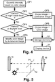
- FIGURE 4 illustrates one suitable algorithm for generating the output image.
- the image intensity is quantified based on the color image. This quanitification can employ an average image intensity, average image intensity per color channel, or other suitable metric.
- the image intensity quantification operation OP1 is performed for sub-regions of the image to enable piecemeal processing of the image.
- the image intensity quantification operation OP1 is optionally replaced by another metric of the color image "quality" such as an image contrast metric.
- the image intensity metric is compared with a intensity night vision level threshold in a comparison operation OP2.
- the objective of this comparison is to determine whether the light intensity is too low for the color image to be useful.
- image “quality” metrics such as image contrast can be used. (In the latter metric, for example, a color image whose image contrast is below a threshold may be assumed to be too dim to be useful). If the comparison operation OP2 indicates that the color image is not useful, then it is assumed that the problem is that the light intensity is too low. In this case, the output image is selected as the acquired luminance image in a selection operation OP3.
- the luminance image has the disadvantage of not being in color (that is, it is a grayscale image)
- the photon counting capability of the set of APD photodetectors APD and associated acquisition circuitry 12 ensures that the luminance image is likely to have useful contrast even in very low light conditions.
- the output image is somewhat analogous to the output of "night vision goggles" or similar devices.
- a second comparison operation OP4 determines whether the color image has intensity corresponding to daylight level. If so, then it is reasonable to assume that the photon counting set of APD photodetectors APD is fully saturated, and accordingly the luminance image is washed out and not useful. In such a case, a second selection operation OP5 selects the color image as the output image.
- a color image modification operation OP6 is performed which adjusts the color image based on corresponding content of the luminance image.
- the modification operation OP6 optionally increases intensity of the red, green, and blue channels of each pixel of the color image by an amount based on the luminance value of the corresponding pixel of the luminance image.
- such intensity enhancement is limited to those regions of the luminance image that have luminance values above a minimum threshold (so that the luminance image is indicating some light is present) and below a maximum threshold (since above such a threshold it may be assumed that the color image successfully captured the higher intensity light).
- a minimum threshold so that the luminance image is indicating some light is present
- a maximum threshold since above such a threshold it may be assumed that the color image successfully captured the higher intensity light.
- Other compositional approaches for modifying the color image based on the luminance image may be used.
- the output image generated by one of the operations OP3, OP5, OP6 is suitably stored in a storage memory 32, displayed on a display device 34, or otherwise utilized.
- the imaging array 10 is a CMOS device
- various components 12, 14, 20, 22, 30, 32, 34 or various combinations of said components may be embodied as separate chips, dies, or so forth, some of which may optionally be fabricated in something other than a silicon-based material system.
- the circuitry components 12, 20, 30 or various portions thereof may be variously embodied as discrete circuitry, integrated circuitry, a suitably programmed microprocessor or microcontroller, or so forth.
- the color imaging device may be a component of, or may be embodied as, substantially any color imaging application device, such as an illustrated digital camera 40 (which may, for example, be a compact digital camera such as are typically used by amateur photographers, or a digital single-lens reflex (SLR) camera such as are typically used by more advanced or professional photographers, or so forth), or a webcam 42 integral with or installed on a computer 44, or so forth.
- the imaging array 10 may view an imaging subject directly, or may be optically coupled with a subject to be imaged by a suitable optical system, such as an illustrated lens 46 of the digital camera 40, or a lens system (not shown) of the webcam 42, or so forth.
- color imaging devices 40, 42 may find application in other application domains such as in medical imaging (for example, as a component of or embodied in an endoscopic device configured for insertion into a subject for internal imaging of the subject under low-light or shadowed conditions), or as a component of or embodied in video equipment for capturing sporting events, and so forth.
- the set of APD photodetectors APD When operated in Geiger mode, the set of APD photodetectors APD extend imaging capability to extremely low light levels, albeit in grayscale. At higher light levels that are still below full daylight illumination, the set of APD photodetectors APD provide a high gain luminance image acquired in Geiger mode or in a less aggressive avalanche multiplication gain mode that can be used to modify or adjust the color image to provide enhanced image contrast or other image enhancement. Because of the high gain provided by the APD photodetectors APD, these substantial advantages can be obtained without replacing a large fraction or percentage of the color-selective photodetectors R, G, B with APD photodetectors APD.
- the APD photodetectors of the set of APD photodetectors make up less than or about one-fourth of the total number of photodetectors of the imaging array.
- the APD photodetectors APD make up precisely one-fourth of the photodetectors of the imaging array.
- FIGURE 5 depicts the color imaging array 10 arranged respective to an optical system 48 to image a subject.
- An optional light source 50 such as a pulsed laser, is coupled into the optical system 48 using a first prism or mirror 52 and a second prism or mirror 54 that is partially reflective and partially transmissive.
- the optional pulsed laser or other light source 50 generates a light pulse that travels through the optical system 48, reflects (at least in part) off of the subject, the (at least partially) reflected light is collected by the optical system 48 and imaged by the imaging array 10.
- the set of APD photodetectors APD operating in Geiger mode are configured with sufficient temporal resolution to detect the delay time between activation of the optional light source 50 and photon counts acquired by the set of APD photodetectors APD responsive to the light pulse generated by activation of the optional light source 50.
- the light source 50 is a pulsed semiconductor laser, pulsed light-emitting diode, or other pulsed narrowband light source, and the APD photodetectors APD are covered by a narrow-band filter tuned to the wavelength of the light source 50 to block ambient light from being detected.
- the prism or mirror 54 is almost completely transmissive for most of the visible spectrum (for example, by being made out of glass or another highly transparent material), but is made partially reflective for the wavelength of the light source 50 by disposing on the prism or mirror 54 dielectric layers defining a narrow-band Bragg reflector tuned to have peak reflectance at the wavelength of the light source 50.
- time-to-digital converters typically employ a substantial number of time-to-digital converters to achieve high depth resolution in the centimeter range. However, if a high depth resolution is not required, then a less complex scheme can be employed.
- the sensor lines are read out sequentially with a well defined time step of typically few nanoseconds. So, the depth difference between two subsequent lines is in the order of few tens of centimeters.
- the time offset between activation of the light source 50 and the start of the APD photodetectors readout the entire depth range is covered by all the lines.
- the scene is illuminated by several millions of short light pulses with slowly increasing time step and frames are collected for every depth of the scene.
- the light pulses can be interleaved with the readouts.
- FIGURE 8 when using the depth estimation scheme of FIGURE 6 or of FIGURE 7 , for each pixel the received photons are suitably collected in depth histograms. Each bin of the histogram contains the number of photons received by the pixel with a time-of-flight less than or equal the depth d .
- FIGURE 8 diagrammatically shows an example of such a histogram for two objects at two different distances. The histogram is plotted using a solid line in FIGURE 8 . The derivative of the histogram is plotted using a dashed line in FIGURE 8 .
- the two peaks in the derivative of the histogram correspond to the depth positions of the two viewed objects (the two viewed objects are either along different lines of sight, or the front object is a transparent object such as a window pane) or two distinct portions of a single viewed object spanning different depth positions. More generally, each peak in the histogram derivative corresponds to the depth of an object.
- the differentiation of the histogram increases the noise. Accordingly, the number of measurements (corresponding to the number of light source activation events and corresponding acquisitions) should be sufficient to provide depth localization of the objects at the desired noise level. Noise reducing signal processing techniques can also be applied.
- the imaging array is a single integrated imaging array in which the APD photodetectors APD are interspersed with the color-selective photodetectors R, G, B.
- This approach facilitates fabrication of a compact color imaging device, and also ensures spatial registration of the acquired color image and the acquired luminance image.
- the integrated approach can make manufacturing more difficult.
- replacing a conventional color imaging array with the integrated imaging array 10 entails modification of both the color imaging array and of coupling electronics of the color image acquisition circuitry.
- an APD photodetectors array APDA is included as an add-on component of an existing color imaging system.
- the existing color imaging system can use a color imaging array with red, green, and blue photodetectors (variation not illustrated), or as illustrated can use a separate red photodetector array RA, green photodetector array GA, and blue photodetector array BA.
- the optical system 48 is again used to capture light from the subject, and partially reflective/partially transmissive prisms or mirrors 60, 62, 64 are used to couple selected fractions of the light from the subject to each of the imaging arrays RA, GA, BA, APDA.
- the color image is acquired by combining the color channel images generated by the respective three color-selective arrays RA, GA, BA, while the luminance image is generated by the APD photodetectors array APDA.
- Remaining components shown in FIGURE 1 such as the digital image processing circuitry 30, can be utilized in the system of FIGURE 9 .
- the optional light source 50 is included for use in acquiring depth information, and is coupled into the optical system 48 via the partially reflective mirror 60 and an additional partially reflective/partially transmissive mirror 66.
- the light source 50 can also be configured to illuminate the subject via an optical pathway that does not include the optical system 48.
- the light source 50 is arranged to directly illuminate the subject without any intervening optics.
Landscapes
- Engineering & Computer Science (AREA)
- Physics & Mathematics (AREA)
- Electromagnetism (AREA)
- Radar, Positioning & Navigation (AREA)
- Remote Sensing (AREA)
- Computer Networks & Wireless Communication (AREA)
- General Physics & Mathematics (AREA)
- Multimedia (AREA)
- Signal Processing (AREA)
- Color Television Image Signal Generators (AREA)
- Solid State Image Pick-Up Elements (AREA)
- Transforming Light Signals Into Electric Signals (AREA)
Claims (13)
- Farbbildgebungsvorrichtung, umfassend:ein oder mehrere Arrays (10, RA, GA, BA) von farbselektiven Fotodetektoren (R, G, B), die konfiguriert sind, um ein Farbbild eines Motivs zu erfassen;Digitale Bildverarbeitungsschaltung (30), die konfiguriert ist, um das Farbbild und/oder ein Luminanzbild auszuwählen, um ein Ausgabebild des Motivs zu erzeugen,wobei die digitale Bildverarbeitungsschaltung (30) konfiguriert ist, umeine Bildintensitätsmetrik auf der Grundlage des Farbbildes zu quantifizieren, unddie Bildintensitätsmetrik mit einem Schwellenwert für die Intensität des Nachtsichtniveaus zu vergleichen und das Ausgabebild als das Luminanzbild des Motivs auszuwählen, wenn die Bildintensitätsmetrik unter dem Schwellenwert für die Intensität des Nachtsichtniveaus liegt,gekennzeichnet durcheinen Satz von Lawinenfotodioden-Fotodetektoren (APD), die angeordnet sind, um das Luminanzbild des Motivs zu erfassen;wobei die digitale Bildverarbeitungsschaltung (30) weiter konfiguriert ist, umdie Bildintensitätsmetrik mit einem Schwellenwert für die Intensität des Tageslichtniveaus zu vergleichen und das Ausgabebild als das Farbbild des Motivs auszuwählen, wenn die Bildintensitätsmetrik über dem Schwellenwert für die Intensität des Nachtsichtniveaus und über dem Schwellenwert für die Intensität des Tageslichtniveaus liegt,ein modifiziertes Farbbild zu erzeugen, indem das Farbbild auf der Grundlage des entsprechenden Inhalts des Luminanzbildes eingestellt wird, und das Ausgabebild als das modifizierte Farbbild des Motivs ausgewählt wird, wenn die Bildintensitätsmetrik über dem Schwellenwert für die Intensität des Nachtsichtniveaus und unter dem Schwellenwert für die Intensität des Tageslichts liegt.
- Farbbildgebungsvorrichtung nach Anspruch 1, wobei die Lawinenfotodioden-Fotodetektoren (APD) zwischen farbselektiven Fotodetektoren (R, G, B) der einen oder mehreren Arrays (10) von farbselektiven Fotodetektoren angeordnet sind.
- Farbbildgebungsvorrichtung nach Anspruch 2, wobei das eine oder die mehreren Arrays (10) von farbselektiven Fotodetektoren ein einzelnes Array von Fotodetektoren mit durchsetzten roten, grünen und blauen Fotodetektoren (R, G, B) umfassen.
- Farbbildgebungsvorrichtung nach Anspruch 3, wobei Lawinenfotodioden-Fotodetektoren (APD) weniger als oder etwa ein Viertel der Gesamtzahl der Fotodetektoren (APD, R, G, B) des Arrays (10) von Fotodetektoren umfassen.
- Farbbildgebungsvorrichtung nach Anspruch 1, wobei der Satz von Lawinenfotodioden-Fotodetektoren (APD) ein Array (APDA) definiert, das von dem einen oder den mehreren Arrays (RA, GA, BA) von farbselektiven Fotodetektoren (R, G, B) getrennt ist.
- Farbbildgebungsvorrichtung nach einem der Ansprüche 1 bis 5, weiter umfassend:
Photonenzählschaltung (12), die die Lawinenfotodioden-Fotodetektoren (APD) im Geiger-Modus betreibt, um das Luminanzbild auf der Grundlage der mit den Lawinenfotodioden-Fotodetektoren erfassten Photonenzählungen zu erzeugen. - Farbbildgebungsvorrichtung nach Anspruch 6, wobei die digitale Bildverarbeitungsschaltung (30) konfiguriert ist, um mindestens einen Teil des erfassten Farbbildes auf der Grundlage eines entsprechenden Teils des erfassten Luminanzbildes einzustellen.
- Farbbildgebungsvorrichtung nach einem der Ansprüche 6 bis 7, wobei die digitale Bildverarbeitungsschaltung (30) konfiguriert ist, um Tiefeninformationen auf der Grundlage der Verzögerungszeit zwischen der Aktivierung einer Lichtquelle (50) und den unter Verwendung der Lawinenfotodioden-Fotodetektoren (APD) erfassten Photonenzählungen zu erzeugen.
- Farbbildgebungsvorrichtung nach einem der Ansprüche 1 bis 8, wobei das eine oder die mehreren Arrays (10, RA, GA, BA) von farbselektiven Fotodetektoren (R, G, B) und der Satz von Lawinenfotodioden-Fotodetektoren (APD) beide CMOS-Vorrichtungen umfassen.
- Farbbildgebungsvorrichtung nach einem der Ansprüche 1 bis 9, weiter umfassend:
Abbildungsoptik (48), die optisch Licht von dem Motiv an das eine oder die mehreren Arrays (10, RA, GA, BA) von farbselektiven Fotodetektoren (R, G, B) und an den Satz von Lawinenfotodioden-Fotodeketoren (APD) koppelt, um die Erfassung des Farbbildes und des Luminanzbildes des Motivs zu ermöglichen. - Farbbildgebungsvorrichtung nach einem der Ansprüche 1 bis 10, wobei die Farbbildgebungsvorrichtung eine Digitalkamera (40) oder eine Webkamera (42) umfasst.
- Farbbildgebungsvorrichtung nach einem der Ansprüche 1 bis 10, wobei die Farbbildgebungsvorrichtung eine medizinische Bildgebungsvorrichtung umfasst.
- Farbbildgebungsverfahren, umfassend:Abbilden eines Motivs unter Verwendung eines oder mehrerer Arrays (10, RA, GA, BA) von farbselektiven Fotodetektoren (R, G, B), die konfiguriert sind, um ein Farbbild eines Motivs und einen Satz Lawinenfotodioden-Fotodetektoren (APD) zu erfassen und angeordnet sind, um ein Luminanzbild des Motivs zu erhalten; undQuantifizieren einer Bildintensitätsmetrik auf der Grundlage des Farbbildes,Vergleichen der Bildintensitätsmetrik mit einem Schwellenwert für die Intensität des Nachtsichtniveaus und Auswählen des Ausgabebildes als das Luminanzbild des Motivs, wenn die Bildintensitätsmetrik unter dem Schwellenwert für die Intensität des Nachtsichtniveaus liegt,Vergleichen der Bildintensitätsmetrik mit einem Schwellenwert für die Intensität des Tageslichtniveaus und Auswählen des Ausgabebildes als Farbbild des Motivs, wenn die Bildintensitätsmetrik über dem Schwellenwert für die Intensität des Nachtsichtniveaus und über dem Schwellenwert für die Intensität des Tageslichtniveaus liegt,Einstellen des Farbbildes auf der Grundlage des entsprechenden Inhalts des Luminanzbildes, um ein modifiziertes Farbbild zu erzeugen und das Ausgabebild als modifiziertes Farbbild des Motivs auszuwählen, wenn die Bildintensitätsmetrik über dem Schwellenwert für die Intensität des Nachtsichtniveaus und unter dem Schwellenwert für die Intensität des Tageslichtniveaus liegt.
Applications Claiming Priority (2)
| Application Number | Priority Date | Filing Date | Title |
|---|---|---|---|
| US13973908P | 2008-12-22 | 2008-12-22 | |
| PCT/IB2009/055194 WO2010073137A1 (en) | 2008-12-22 | 2009-11-19 | Cmos imager with single photon counting capability |
Publications (2)
| Publication Number | Publication Date |
|---|---|
| EP2380038A1 EP2380038A1 (de) | 2011-10-26 |
| EP2380038B1 true EP2380038B1 (de) | 2019-01-09 |
Family
ID=41667181
Family Applications (1)
| Application Number | Title | Priority Date | Filing Date |
|---|---|---|---|
| EP09774935.2A Not-in-force EP2380038B1 (de) | 2008-12-22 | 2009-11-19 | Cmos bildaufnehmer |
Country Status (5)
| Country | Link |
|---|---|
| US (1) | US8610808B2 (de) |
| EP (1) | EP2380038B1 (de) |
| JP (1) | JP2012513694A (de) |
| CN (1) | CN102265176B (de) |
| WO (1) | WO2010073137A1 (de) |
Families Citing this family (43)
| Publication number | Priority date | Publication date | Assignee | Title |
|---|---|---|---|---|
| US8716643B2 (en) * | 2010-09-06 | 2014-05-06 | King Abdulaziz City Science And Technology | Single photon counting image sensor and method |
| US9052497B2 (en) | 2011-03-10 | 2015-06-09 | King Abdulaziz City For Science And Technology | Computing imaging data using intensity correlation interferometry |
| US9099214B2 (en) | 2011-04-19 | 2015-08-04 | King Abdulaziz City For Science And Technology | Controlling microparticles through a light field having controllable intensity and periodicity of maxima thereof |
| ITTO20110689A1 (it) * | 2011-07-28 | 2013-01-29 | St Microelectronics Srl | Spettrometro includente un fotodiodo a valanga operante in modalita' geiger |
| JP6059722B2 (ja) | 2011-08-03 | 2017-01-11 | コーニンクレッカ フィリップス エヌ ヴェKoninklijke Philips N.V. | デジタルシリコン光電子増倍管アレイに関する位置敏感な読み出しモード |
| US8471205B2 (en) * | 2011-08-25 | 2013-06-25 | Bae Systems Information And Electronic Systems Integration Inc. | Hybrid photodiode/APD focal plane array for solid state low light level imagers |
| WO2013066959A1 (en) * | 2011-10-31 | 2013-05-10 | The Trustees Of Columbia University In The City Of New York | Systems and methods for imaging using single photon avalanche diodes |
| US8736008B2 (en) | 2012-01-04 | 2014-05-27 | General Electric Company | Photodiode array and methods of fabrication |
| US20150049177A1 (en) * | 2012-02-06 | 2015-02-19 | Biooptico Ab | Camera Arrangement and Image Processing Method for Quantifying Tissue Structure and Degeneration |
| EP2822270A1 (de) * | 2012-02-27 | 2015-01-07 | Sony Corporation | Bildaufzeichnungselement und elektronische vorrichtung damit |
| CN102662165A (zh) * | 2012-05-24 | 2012-09-12 | 中国科学院光电研究院 | 主被动复合阵列式光电探测装置 |
| WO2014018936A2 (en) | 2012-07-26 | 2014-01-30 | Olive Medical Corporation | Continuous video in a light deficient environment |
| CA2878514A1 (en) | 2012-07-26 | 2014-01-30 | Olive Medical Corporation | Ycbcr pulsed illumination scheme in a light deficient environment |
| US9036065B1 (en) | 2012-08-16 | 2015-05-19 | Rambus Inc. | Shared-counter image sensor |
| US9679929B2 (en) | 2012-10-12 | 2017-06-13 | Samsung Electronics Co., Ltd. | Binary image sensors including quantum dots and unit pixels thereof |
| US9432604B2 (en) | 2012-10-12 | 2016-08-30 | Samsung Electronics Co., Ltd. | Image sensor chips |
| CA2902319A1 (en) | 2013-02-28 | 2014-09-04 | Olive Medical Corporation | Videostroboscopy of vocal chords with cmos sensors |
| CA2906798A1 (en) | 2013-03-15 | 2014-09-18 | Olive Medical Corporation | Super resolution and color motion artifact correction in a pulsed color imaging system |
| US9777913B2 (en) | 2013-03-15 | 2017-10-03 | DePuy Synthes Products, Inc. | Controlling the integral light energy of a laser pulse |
| EP2967301B1 (de) | 2013-03-15 | 2021-11-03 | DePuy Synthes Products, Inc. | Bereichsmessung in einer lichtkontrollierten umgebung |
| EP3119265B1 (de) | 2014-03-21 | 2019-09-11 | DePuy Synthes Products, Inc. | Kartenrandstecker für abbildungssensoren |
| EP2955544B1 (de) * | 2014-06-11 | 2020-06-17 | Sony Depthsensing Solutions N.V. | TOF-Kamerasystem und Verfahren zum Messen einer Entfernung mit dem System |
| CN104075802B (zh) * | 2014-07-09 | 2016-01-06 | 南京发艾博光电科技有限公司 | 一种高动态范围的光子计数型微弱光信号测量装置及方法 |
| CN104796674A (zh) * | 2015-04-17 | 2015-07-22 | 南京理工大学 | 基于压缩感知的彩色成像装置及方法 |
| WO2017038542A1 (ja) * | 2015-09-03 | 2017-03-09 | ソニーセミコンダクタソリューションズ株式会社 | 固体撮像素子、および電子装置 |
| US10381502B2 (en) | 2015-09-09 | 2019-08-13 | Teledyne Scientific & Imaging, Llc | Multicolor imaging device using avalanche photodiode |
| JP2017075906A (ja) * | 2015-10-16 | 2017-04-20 | 浜松ホトニクス株式会社 | 測距装置 |
| CN108291961B (zh) * | 2015-12-08 | 2022-06-28 | 松下知识产权经营株式会社 | 固体摄像装置、距离测定装置及距离测定方法 |
| KR20200028446A (ko) | 2017-08-31 | 2020-03-16 | 에스지 디제이아이 테크놀러지 코., 엘티디 | 고체 상태 광 검출 및 레인징(lidar) 시스템, 그리고 고체 상태 광 검출 및 레이징(lidar) 분해능을 향상시키는 시스템 및 방법 |
| WO2019041267A1 (en) * | 2017-08-31 | 2019-03-07 | SZ DJI Technology Co., Ltd. | SYSTEMS AND METHODS FOR SOLID LASER RADAR TO APD NETWORK SEMICONDUCTOR |
| JP6862386B2 (ja) | 2018-03-22 | 2021-04-21 | 株式会社東芝 | 光検出器、ライダー装置、及び光検出器の製造方法 |
| WO2019225224A1 (ja) * | 2018-05-24 | 2019-11-28 | ソニーセミコンダクタソリューションズ株式会社 | 時間計測装置 |
| US11054546B2 (en) | 2018-07-16 | 2021-07-06 | Faro Technologies, Inc. | Laser scanner with enhanced dymanic range imaging |
| JP7114396B2 (ja) | 2018-08-03 | 2022-08-08 | キヤノン株式会社 | 撮像装置、撮像システム、移動体 |
| US11272112B2 (en) | 2018-08-08 | 2022-03-08 | Canon Kabushiki Kaisha | Image capturing apparatus |
| JP7293002B2 (ja) * | 2018-08-08 | 2023-06-19 | キヤノン株式会社 | 撮像装置 |
| CN112585953B (zh) * | 2018-09-06 | 2024-05-14 | 松下知识产权经营株式会社 | 固体摄像元件、摄像系统、固体摄像元件的驱动方法及光检测器 |
| JP7218193B2 (ja) * | 2019-01-31 | 2023-02-06 | キヤノン株式会社 | 撮像装置 |
| JP7562282B2 (ja) * | 2019-06-28 | 2024-10-07 | キヤノン株式会社 | 撮像表示装置、およびウェアラブルデバイス |
| WO2022064576A1 (ja) * | 2020-09-23 | 2022-03-31 | 株式会社ソニー・インタラクティブエンタテインメント | 位置情報取得装置、ヘッドマウントディスプレイ、および位置情報取得方法 |
| US11624653B2 (en) | 2020-12-03 | 2023-04-11 | Artilux, Inc. | Multi-application optical sensing apparatus and method thereof |
| FR3160840A1 (fr) * | 2024-03-29 | 2025-10-03 | Stmicroelectronics International N.V. | Camera a deux images natives de sortie |
| CN118354220B (zh) * | 2024-04-16 | 2025-05-13 | 中国科学院国家空间科学中心 | 一种基于icmos的自适应多模式紫外成像探测系统 |
Citations (2)
| Publication number | Priority date | Publication date | Assignee | Title |
|---|---|---|---|---|
| EP0354382A1 (de) * | 1988-07-20 | 1990-02-14 | Geutebrück Videotechnik Gmbh | Optische Überwachungseinrichtung |
| EP1973160A2 (de) * | 2007-03-22 | 2008-09-24 | Kabushiki Kaisha Toshiba | Bildsensor, Farbbildsensor mit einer Platte und elektronische Vorrichtung |
Family Cites Families (55)
| Publication number | Priority date | Publication date | Assignee | Title |
|---|---|---|---|---|
| US4003655A (en) * | 1975-04-17 | 1977-01-18 | The United States Of America As Represented By The Secretary Of The Army | Hybrid silicon avalanche quadrant detector |
| US4366377A (en) * | 1980-09-29 | 1982-12-28 | Mcdonnell Douglas Corporation | Dual sensitivity optical sensor |
| US4616247A (en) * | 1983-11-10 | 1986-10-07 | At&T Bell Laboratories | P-I-N and avalanche photodiodes |
| JPH0799868B2 (ja) * | 1984-12-26 | 1995-10-25 | 日本放送協会 | 固体撮像装置 |
| JPH0716256B2 (ja) * | 1985-12-18 | 1995-02-22 | ソニー株式会社 | 電子スチルカメラの記録回路 |
| JPS63131292U (de) * | 1987-02-12 | 1988-08-26 | ||
| US5323233A (en) * | 1990-07-31 | 1994-06-21 | Canon Kabushiki Kaisha | Image signal processing apparatus having a color filter with offset luminance filter elements |
| GB2345217A (en) * | 1998-12-23 | 2000-06-28 | Nokia Mobile Phones Ltd | Colour video image sensor |
| US6555890B2 (en) * | 2000-05-23 | 2003-04-29 | Sensors Unlimited, Inc. | Method for combined fabrication of indium gallium arsenide/indium phosphide avalanche photodiodes and p-i-n photodiodes |
| WO2001092870A2 (de) * | 2000-06-02 | 2001-12-06 | Zeptosens Ag | Kit und verfahren zur multianalytbestimmung |
| JP3949360B2 (ja) * | 2000-08-29 | 2007-07-25 | 日本放送協会 | カラーイメージセンサ |
| US6774578B2 (en) * | 2000-09-19 | 2004-08-10 | Semiconductor Energy Laboratory Co., Ltd. | Self light emitting device and method of driving thereof |
| US20030048493A1 (en) * | 2001-09-10 | 2003-03-13 | Pontifex Brian Decoursey | Two sensor quantitative low-light color camera |
| US20040178463A1 (en) * | 2002-03-20 | 2004-09-16 | Foveon, Inc. | Vertical color filter sensor group with carrier-collection elements of different size and method for fabricating such a sensor group |
| US6841816B2 (en) * | 2002-03-20 | 2005-01-11 | Foveon, Inc. | Vertical color filter sensor group with non-sensor filter and method for fabricating such a sensor group |
| US6658329B1 (en) | 2002-05-02 | 2003-12-02 | The United States Of America As Represented By The United States National Aeronautics And Space Administration | Video guidance sensor system with laser rangefinder |
| JP4135486B2 (ja) * | 2002-12-06 | 2008-08-20 | 日本ビクター株式会社 | イメージセンサ |
| JP4465958B2 (ja) * | 2002-12-18 | 2010-05-26 | 株式会社ニコン | カラー撮像装置 |
| US6914314B2 (en) * | 2003-01-31 | 2005-07-05 | Foveon, Inc. | Vertical color filter sensor group including semiconductor other than crystalline silicon and method for fabricating same |
| US6894265B2 (en) * | 2003-01-31 | 2005-05-17 | Foveon, Inc. | Vertical color filter sensor group and semiconductor integrated circuit fabrication method for fabricating same |
| JP2005006856A (ja) * | 2003-06-18 | 2005-01-13 | Olympus Corp | 内視鏡装置 |
| US20060226374A1 (en) * | 2003-08-06 | 2006-10-12 | Gnothis Holding S.A. | Method and device for identifying luminescent molecules according to the fluorescence correlation spectroscopy method |
| JP2005093610A (ja) * | 2003-09-16 | 2005-04-07 | Sumitomo Electric Ind Ltd | 光受信器 |
| JP2005183538A (ja) * | 2003-12-17 | 2005-07-07 | Sumitomo Electric Ind Ltd | 受光素子及び光受信器 |
| US7515082B2 (en) * | 2003-12-19 | 2009-04-07 | Searete, Llc | Photo-detector filter having a cascaded low noise amplifier |
| US7683308B2 (en) * | 2004-01-12 | 2010-03-23 | Ecole Polytechnique Federale de Lausanne EFPL | Controlling spectral response of photodetector for an image sensor |
| EP1594321A3 (de) * | 2004-05-07 | 2006-01-25 | Dialog Semiconductor GmbH | Farbbildaufnahmevorrichtung mit erweitertem Dynamikbereich |
| WO2005115005A2 (en) * | 2004-05-20 | 2005-12-01 | Board Of Regents Of The University & Community College Of Nevada, Reno | Photon event distribution sampling apparatus and method |
| US7880785B2 (en) | 2004-07-21 | 2011-02-01 | Aptina Imaging Corporation | Rod and cone response sensor |
| EP1794797B1 (de) * | 2004-07-28 | 2015-09-09 | Quantum Semiconductor, LLC | Layouts zur monolithischen integration von cmos und abgelagerten photonischen aktivschichten |
| US7477304B2 (en) * | 2004-08-26 | 2009-01-13 | Micron Technology, Inc. | Two narrow band and one wide band color filter for increasing color image sensor sensitivity |
| US7653427B2 (en) * | 2004-11-12 | 2010-01-26 | Intra-Medical Imaging LLC | Method and instrument for minimally invasive sentinel lymph node location and biopsy |
| EP1679907A1 (de) * | 2005-01-05 | 2006-07-12 | Dialog Semiconductor GmbH | Hexagonale Farbpixel-Struktur mit weissen Pixeln |
| US7547872B2 (en) * | 2005-02-14 | 2009-06-16 | Ecole Polytechnique Federale De Lausanne | Integrated circuit comprising an array of single photon avalanche diodes |
| US7262402B2 (en) * | 2005-02-14 | 2007-08-28 | Ecole Polytechnique Federal De Lausanne | Integrated imager circuit comprising a monolithic array of single photon avalanche diodes |
| WO2006104201A1 (ja) * | 2005-03-29 | 2006-10-05 | Olympus Corporation | 細胞画像解析方法、細胞画像解析プログラム、細胞画像解析装置、スクリーニング方法およびスクリーニング装置 |
| US20060268357A1 (en) * | 2005-05-25 | 2006-11-30 | Vook Dietrich W | System and method for processing images using centralized image correction data |
| WO2006127967A2 (en) * | 2005-05-25 | 2006-11-30 | Massachusetts Institute Of Technology | Multifocal scanning microscopy systems and methods |
| US20070012948A1 (en) * | 2005-07-15 | 2007-01-18 | Dries J C | Combined APD / PIN InGaAs photodetector with microlens structure and method of manufacture |
| WO2007038600A2 (en) * | 2005-09-27 | 2007-04-05 | Northwestern University | A single-photon detector and applications of same |
| US7714292B2 (en) * | 2006-02-01 | 2010-05-11 | Koninklijke Philips Electronics N.V. | Geiger mode avalanche photodiode |
| JP4846409B2 (ja) * | 2006-03-30 | 2011-12-28 | 富士フイルム株式会社 | 固体撮像装置 |
| JP5106870B2 (ja) * | 2006-06-14 | 2012-12-26 | 株式会社東芝 | 固体撮像素子 |
| EP2044420A2 (de) * | 2006-07-17 | 2009-04-08 | Max Wiki | Analytisches system mit einer anordnung zur zeitlich veränderbaren räumlichen lichtmodulation und damit ausführbares nachweisverfahren |
| US8187541B2 (en) | 2006-09-18 | 2012-05-29 | California Institute Of Technology | Apparatus for detecting target molecules and related methods |
| US7769229B2 (en) | 2006-11-30 | 2010-08-03 | Eastman Kodak Company | Processing images having color and panchromatic pixels |
| US7893976B2 (en) | 2006-12-01 | 2011-02-22 | Eastman Kodak Company | Light sensitivity in image sensors |
| JP2008193163A (ja) * | 2007-01-31 | 2008-08-21 | Sanyo Electric Co Ltd | 固体撮像装置 |
| JP4930109B2 (ja) * | 2007-03-06 | 2012-05-16 | ソニー株式会社 | 固体撮像装置、撮像装置 |
| TWI334732B (en) * | 2007-03-16 | 2010-12-11 | Coretronic Corp | Projector and method for adjusting projective luminance thereof |
| US20080240543A1 (en) * | 2007-03-30 | 2008-10-02 | Wolfgang Ernst Gustav Budach | Calibration and normalization method for biosensors |
| JP2008306379A (ja) | 2007-06-06 | 2008-12-18 | Toshiba Corp | 固体撮像素子 |
| US20090060381A1 (en) * | 2007-08-31 | 2009-03-05 | Ethicon Endo-Surgery, Inc. | Dynamic range and amplitude control for imaging |
| US8227884B2 (en) * | 2009-11-04 | 2012-07-24 | Omnivision Technologies, Inc. | Photodetector array having array of discrete electron repulsive elements |
| US20110101201A1 (en) * | 2009-11-04 | 2011-05-05 | Vincent Venezia | Photodetector Array Having Electron Lens |
-
2009
- 2009-11-19 WO PCT/IB2009/055194 patent/WO2010073137A1/en not_active Ceased
- 2009-11-19 CN CN200980152142.7A patent/CN102265176B/zh not_active Expired - Fee Related
- 2009-11-19 US US13/139,626 patent/US8610808B2/en not_active Expired - Fee Related
- 2009-11-19 EP EP09774935.2A patent/EP2380038B1/de not_active Not-in-force
- 2009-11-19 JP JP2011541648A patent/JP2012513694A/ja active Pending
Patent Citations (2)
| Publication number | Priority date | Publication date | Assignee | Title |
|---|---|---|---|---|
| EP0354382A1 (de) * | 1988-07-20 | 1990-02-14 | Geutebrück Videotechnik Gmbh | Optische Überwachungseinrichtung |
| EP1973160A2 (de) * | 2007-03-22 | 2008-09-24 | Kabushiki Kaisha Toshiba | Bildsensor, Farbbildsensor mit einer Platte und elektronische Vorrichtung |
Also Published As
| Publication number | Publication date |
|---|---|
| WO2010073137A1 (en) | 2010-07-01 |
| CN102265176A (zh) | 2011-11-30 |
| US8610808B2 (en) | 2013-12-17 |
| EP2380038A1 (de) | 2011-10-26 |
| US20110249148A1 (en) | 2011-10-13 |
| CN102265176B (zh) | 2015-09-30 |
| JP2012513694A (ja) | 2012-06-14 |
Similar Documents
| Publication | Publication Date | Title |
|---|---|---|
| EP2380038B1 (de) | Cmos bildaufnehmer | |
| US7119842B2 (en) | Image capturing device including a spectrally-selectively transmissive diaphragm | |
| CN102970480B (zh) | 图像拍摄装置及其控制方法 | |
| KR102165399B1 (ko) | 센서 노출들 사이의 최소화된 지연 시간을 갖는 게이트된 센서 기반 이미징 시스템 | |
| JP6243402B2 (ja) | 読み出し毎の複数のゲーテッド画素 | |
| US20100171875A1 (en) | Imager capturing an image with a rolling shutter | |
| US11936987B2 (en) | Image capturing apparatus | |
| KR20200096828A (ko) | 물체까지의 거리를 결정하기 위한 시스템 및 방법 | |
| US7295241B2 (en) | Image capturing apparatus, image capturing method, and computer-readable medium storing a program for an image capturing apparatus | |
| CN102292974A (zh) | 摄像设备 | |
| JP2004309701A (ja) | 測距測光用センサ及びカメラ | |
| KR20240093789A (ko) | 포토닉스 시스템 및 방법 | |
| JP7293002B2 (ja) | 撮像装置 | |
| RU59923U1 (ru) | Пзс-видеокамера | |
| US8681263B2 (en) | Imager capturing an image with a rolling shutter using flicker detection | |
| US20190246053A1 (en) | Motion tracking using multiple exposures | |
| EP2471256B1 (de) | Digitales kamerasystem und verfahren | |
| US8520128B2 (en) | Auto focus module capable of in-pixel monitoring of amount of received light photographing apparatus using the same | |
| EP3335417B1 (de) | Digitale integrierte ausleseschaltung mit abweisung einer modulierten lichtquelle | |
| TWI795903B (zh) | 光子系統及方法 | |
| WO2024101034A1 (ja) | オートフォーカス制御装置、撮像装置、オートフォーカス制御方法、およびプログラム | |
| WO2024127782A1 (ja) | 光検出システム、撮像装置、制御方法 | |
| WO2025243215A1 (en) | Method for controlling the discharge of a photosensitive element in a photodetector and photodetector thereof | |
| JP2025030679A (ja) | 撮像装置、方法及びプログラム | |
| JP2008066352A (ja) | 半導体装置 |
Legal Events
| Date | Code | Title | Description |
|---|---|---|---|
| PUAI | Public reference made under article 153(3) epc to a published international application that has entered the european phase |
Free format text: ORIGINAL CODE: 0009012 |
|
| 17P | Request for examination filed |
Effective date: 20110722 |
|
| AK | Designated contracting states |
Kind code of ref document: A1 Designated state(s): AT BE BG CH CY CZ DE DK EE ES FI FR GB GR HR HU IE IS IT LI LT LU LV MC MK MT NL NO PL PT RO SE SI SK SM TR |
|
| DAX | Request for extension of the european patent (deleted) | ||
| RAP1 | Party data changed (applicant data changed or rights of an application transferred) |
Owner name: KONINKLIJKE PHILIPS N.V. Owner name: PHILIPS INTELLECTUAL PROPERTY & STANDARDS GMBH |
|
| 17Q | First examination report despatched |
Effective date: 20150717 |
|
| STAA | Information on the status of an ep patent application or granted ep patent |
Free format text: STATUS: EXAMINATION IS IN PROGRESS |
|
| REG | Reference to a national code |
Ref country code: DE Ref legal event code: R079 Ref document number: 602009056649 Country of ref document: DE Free format text: PREVIOUS MAIN CLASS: G01S0011000000 Ipc: H04N0005369000 |
|
| GRAP | Despatch of communication of intention to grant a patent |
Free format text: ORIGINAL CODE: EPIDOSNIGR1 |
|
| STAA | Information on the status of an ep patent application or granted ep patent |
Free format text: STATUS: GRANT OF PATENT IS INTENDED |
|
| RIC1 | Information provided on ipc code assigned before grant |
Ipc: H04N 5/369 20110101AFI20180711BHEP Ipc: H04N 9/04 20060101ALI20180711BHEP |
|
| INTG | Intention to grant announced |
Effective date: 20180723 |
|
| GRAS | Grant fee paid |
Free format text: ORIGINAL CODE: EPIDOSNIGR3 |
|
| GRAA | (expected) grant |
Free format text: ORIGINAL CODE: 0009210 |
|
| STAA | Information on the status of an ep patent application or granted ep patent |
Free format text: STATUS: THE PATENT HAS BEEN GRANTED |
|
| AK | Designated contracting states |
Kind code of ref document: B1 Designated state(s): AT BE BG CH CY CZ DE DK EE ES FI FR GB GR HR HU IE IS IT LI LT LU LV MC MK MT NL NO PL PT RO SE SI SK SM TR |
|
| REG | Reference to a national code |
Ref country code: GB Ref legal event code: FG4D |
|
| REG | Reference to a national code |
Ref country code: CH Ref legal event code: EP Ref country code: AT Ref legal event code: REF Ref document number: 1088773 Country of ref document: AT Kind code of ref document: T Effective date: 20190115 |
|
| REG | Reference to a national code |
Ref country code: DE Ref legal event code: R096 Ref document number: 602009056649 Country of ref document: DE |
|
| REG | Reference to a national code |
Ref country code: IE Ref legal event code: FG4D |
|
| REG | Reference to a national code |
Ref country code: NL Ref legal event code: MP Effective date: 20190109 |
|
| REG | Reference to a national code |
Ref country code: LT Ref legal event code: MG4D |
|
| PG25 | Lapsed in a contracting state [announced via postgrant information from national office to epo] |
Ref country code: NL Free format text: LAPSE BECAUSE OF FAILURE TO SUBMIT A TRANSLATION OF THE DESCRIPTION OR TO PAY THE FEE WITHIN THE PRESCRIBED TIME-LIMIT Effective date: 20190109 |
|
| REG | Reference to a national code |
Ref country code: AT Ref legal event code: MK05 Ref document number: 1088773 Country of ref document: AT Kind code of ref document: T Effective date: 20190109 |
|
| PG25 | Lapsed in a contracting state [announced via postgrant information from national office to epo] |
Ref country code: FI Free format text: LAPSE BECAUSE OF FAILURE TO SUBMIT A TRANSLATION OF THE DESCRIPTION OR TO PAY THE FEE WITHIN THE PRESCRIBED TIME-LIMIT Effective date: 20190109 Ref country code: NO Free format text: LAPSE BECAUSE OF FAILURE TO SUBMIT A TRANSLATION OF THE DESCRIPTION OR TO PAY THE FEE WITHIN THE PRESCRIBED TIME-LIMIT Effective date: 20190409 Ref country code: ES Free format text: LAPSE BECAUSE OF FAILURE TO SUBMIT A TRANSLATION OF THE DESCRIPTION OR TO PAY THE FEE WITHIN THE PRESCRIBED TIME-LIMIT Effective date: 20190109 Ref country code: SE Free format text: LAPSE BECAUSE OF FAILURE TO SUBMIT A TRANSLATION OF THE DESCRIPTION OR TO PAY THE FEE WITHIN THE PRESCRIBED TIME-LIMIT Effective date: 20190109 Ref country code: PT Free format text: LAPSE BECAUSE OF FAILURE TO SUBMIT A TRANSLATION OF THE DESCRIPTION OR TO PAY THE FEE WITHIN THE PRESCRIBED TIME-LIMIT Effective date: 20190509 Ref country code: PL Free format text: LAPSE BECAUSE OF FAILURE TO SUBMIT A TRANSLATION OF THE DESCRIPTION OR TO PAY THE FEE WITHIN THE PRESCRIBED TIME-LIMIT Effective date: 20190109 Ref country code: LT Free format text: LAPSE BECAUSE OF FAILURE TO SUBMIT A TRANSLATION OF THE DESCRIPTION OR TO PAY THE FEE WITHIN THE PRESCRIBED TIME-LIMIT Effective date: 20190109 |
|
| PG25 | Lapsed in a contracting state [announced via postgrant information from national office to epo] |
Ref country code: LV Free format text: LAPSE BECAUSE OF FAILURE TO SUBMIT A TRANSLATION OF THE DESCRIPTION OR TO PAY THE FEE WITHIN THE PRESCRIBED TIME-LIMIT Effective date: 20190109 Ref country code: HR Free format text: LAPSE BECAUSE OF FAILURE TO SUBMIT A TRANSLATION OF THE DESCRIPTION OR TO PAY THE FEE WITHIN THE PRESCRIBED TIME-LIMIT Effective date: 20190109 Ref country code: BG Free format text: LAPSE BECAUSE OF FAILURE TO SUBMIT A TRANSLATION OF THE DESCRIPTION OR TO PAY THE FEE WITHIN THE PRESCRIBED TIME-LIMIT Effective date: 20190409 Ref country code: IS Free format text: LAPSE BECAUSE OF FAILURE TO SUBMIT A TRANSLATION OF THE DESCRIPTION OR TO PAY THE FEE WITHIN THE PRESCRIBED TIME-LIMIT Effective date: 20190509 Ref country code: GR Free format text: LAPSE BECAUSE OF FAILURE TO SUBMIT A TRANSLATION OF THE DESCRIPTION OR TO PAY THE FEE WITHIN THE PRESCRIBED TIME-LIMIT Effective date: 20190410 |
|
| REG | Reference to a national code |
Ref country code: DE Ref legal event code: R097 Ref document number: 602009056649 Country of ref document: DE |
|
| PG25 | Lapsed in a contracting state [announced via postgrant information from national office to epo] |
Ref country code: AT Free format text: LAPSE BECAUSE OF FAILURE TO SUBMIT A TRANSLATION OF THE DESCRIPTION OR TO PAY THE FEE WITHIN THE PRESCRIBED TIME-LIMIT Effective date: 20190109 Ref country code: DK Free format text: LAPSE BECAUSE OF FAILURE TO SUBMIT A TRANSLATION OF THE DESCRIPTION OR TO PAY THE FEE WITHIN THE PRESCRIBED TIME-LIMIT Effective date: 20190109 Ref country code: EE Free format text: LAPSE BECAUSE OF FAILURE TO SUBMIT A TRANSLATION OF THE DESCRIPTION OR TO PAY THE FEE WITHIN THE PRESCRIBED TIME-LIMIT Effective date: 20190109 Ref country code: RO Free format text: LAPSE BECAUSE OF FAILURE TO SUBMIT A TRANSLATION OF THE DESCRIPTION OR TO PAY THE FEE WITHIN THE PRESCRIBED TIME-LIMIT Effective date: 20190109 Ref country code: IT Free format text: LAPSE BECAUSE OF FAILURE TO SUBMIT A TRANSLATION OF THE DESCRIPTION OR TO PAY THE FEE WITHIN THE PRESCRIBED TIME-LIMIT Effective date: 20190109 Ref country code: CZ Free format text: LAPSE BECAUSE OF FAILURE TO SUBMIT A TRANSLATION OF THE DESCRIPTION OR TO PAY THE FEE WITHIN THE PRESCRIBED TIME-LIMIT Effective date: 20190109 Ref country code: SK Free format text: LAPSE BECAUSE OF FAILURE TO SUBMIT A TRANSLATION OF THE DESCRIPTION OR TO PAY THE FEE WITHIN THE PRESCRIBED TIME-LIMIT Effective date: 20190109 |
|
| PLBE | No opposition filed within time limit |
Free format text: ORIGINAL CODE: 0009261 |
|
| STAA | Information on the status of an ep patent application or granted ep patent |
Free format text: STATUS: NO OPPOSITION FILED WITHIN TIME LIMIT |
|
| PG25 | Lapsed in a contracting state [announced via postgrant information from national office to epo] |
Ref country code: SM Free format text: LAPSE BECAUSE OF FAILURE TO SUBMIT A TRANSLATION OF THE DESCRIPTION OR TO PAY THE FEE WITHIN THE PRESCRIBED TIME-LIMIT Effective date: 20190109 |
|
| 26N | No opposition filed |
Effective date: 20191010 |
|
| PG25 | Lapsed in a contracting state [announced via postgrant information from national office to epo] |
Ref country code: SI Free format text: LAPSE BECAUSE OF FAILURE TO SUBMIT A TRANSLATION OF THE DESCRIPTION OR TO PAY THE FEE WITHIN THE PRESCRIBED TIME-LIMIT Effective date: 20190109 |
|
| PG25 | Lapsed in a contracting state [announced via postgrant information from national office to epo] |
Ref country code: TR Free format text: LAPSE BECAUSE OF FAILURE TO SUBMIT A TRANSLATION OF THE DESCRIPTION OR TO PAY THE FEE WITHIN THE PRESCRIBED TIME-LIMIT Effective date: 20190109 |
|
| REG | Reference to a national code |
Ref country code: CH Ref legal event code: PL |
|
| PG25 | Lapsed in a contracting state [announced via postgrant information from national office to epo] |
Ref country code: LU Free format text: LAPSE BECAUSE OF NON-PAYMENT OF DUE FEES Effective date: 20191119 Ref country code: MC Free format text: LAPSE BECAUSE OF FAILURE TO SUBMIT A TRANSLATION OF THE DESCRIPTION OR TO PAY THE FEE WITHIN THE PRESCRIBED TIME-LIMIT Effective date: 20190109 Ref country code: LI Free format text: LAPSE BECAUSE OF NON-PAYMENT OF DUE FEES Effective date: 20191130 Ref country code: CH Free format text: LAPSE BECAUSE OF NON-PAYMENT OF DUE FEES Effective date: 20191130 |
|
| REG | Reference to a national code |
Ref country code: BE Ref legal event code: MM Effective date: 20191130 |
|
| PG25 | Lapsed in a contracting state [announced via postgrant information from national office to epo] |
Ref country code: IE Free format text: LAPSE BECAUSE OF NON-PAYMENT OF DUE FEES Effective date: 20191119 |
|
| PG25 | Lapsed in a contracting state [announced via postgrant information from national office to epo] |
Ref country code: BE Free format text: LAPSE BECAUSE OF NON-PAYMENT OF DUE FEES Effective date: 20191130 |
|
| REG | Reference to a national code |
Ref country code: DE Ref legal event code: R081 Ref document number: 602009056649 Country of ref document: DE Owner name: PHILIPS GMBH, DE Free format text: FORMER OWNER: PHILIPS INTELLECTUAL PROPERTY & STANDARDS, 20099 HAMBURG, DE |
|
| PG25 | Lapsed in a contracting state [announced via postgrant information from national office to epo] |
Ref country code: CY Free format text: LAPSE BECAUSE OF FAILURE TO SUBMIT A TRANSLATION OF THE DESCRIPTION OR TO PAY THE FEE WITHIN THE PRESCRIBED TIME-LIMIT Effective date: 20190109 |
|
| PG25 | Lapsed in a contracting state [announced via postgrant information from national office to epo] |
Ref country code: HU Free format text: LAPSE BECAUSE OF FAILURE TO SUBMIT A TRANSLATION OF THE DESCRIPTION OR TO PAY THE FEE WITHIN THE PRESCRIBED TIME-LIMIT; INVALID AB INITIO Effective date: 20091119 Ref country code: MT Free format text: LAPSE BECAUSE OF FAILURE TO SUBMIT A TRANSLATION OF THE DESCRIPTION OR TO PAY THE FEE WITHIN THE PRESCRIBED TIME-LIMIT Effective date: 20190109 |
|
| PG25 | Lapsed in a contracting state [announced via postgrant information from national office to epo] |
Ref country code: MK Free format text: LAPSE BECAUSE OF FAILURE TO SUBMIT A TRANSLATION OF THE DESCRIPTION OR TO PAY THE FEE WITHIN THE PRESCRIBED TIME-LIMIT Effective date: 20190109 |
|
| REG | Reference to a national code |
Ref country code: DE Ref legal event code: R079 Ref document number: 602009056649 Country of ref document: DE Free format text: PREVIOUS MAIN CLASS: H04N0005369000 Ipc: H04N0025700000 |
|
| PGFP | Annual fee paid to national office [announced via postgrant information from national office to epo] |
Ref country code: GB Payment date: 20221122 Year of fee payment: 14 Ref country code: FR Payment date: 20221122 Year of fee payment: 14 Ref country code: DE Payment date: 20220628 Year of fee payment: 14 |
|
| REG | Reference to a national code |
Ref country code: DE Ref legal event code: R119 Ref document number: 602009056649 Country of ref document: DE |
|
| GBPC | Gb: european patent ceased through non-payment of renewal fee |
Effective date: 20231119 |
|
| PG25 | Lapsed in a contracting state [announced via postgrant information from national office to epo] |
Ref country code: DE Free format text: LAPSE BECAUSE OF NON-PAYMENT OF DUE FEES Effective date: 20240601 |
|
| PG25 | Lapsed in a contracting state [announced via postgrant information from national office to epo] |
Ref country code: GB Free format text: LAPSE BECAUSE OF NON-PAYMENT OF DUE FEES Effective date: 20231119 |
|
| PG25 | Lapsed in a contracting state [announced via postgrant information from national office to epo] |
Ref country code: FR Free format text: LAPSE BECAUSE OF NON-PAYMENT OF DUE FEES Effective date: 20231130 |
|
| PG25 | Lapsed in a contracting state [announced via postgrant information from national office to epo] |
Ref country code: GB Free format text: LAPSE BECAUSE OF NON-PAYMENT OF DUE FEES Effective date: 20231119 Ref country code: FR Free format text: LAPSE BECAUSE OF NON-PAYMENT OF DUE FEES Effective date: 20231130 Ref country code: DE Free format text: LAPSE BECAUSE OF NON-PAYMENT OF DUE FEES Effective date: 20240601 |