EP2380394B1 - Plaque de cuisson à induction comprenant au moins un onduleur - Google Patents
Plaque de cuisson à induction comprenant au moins un onduleur Download PDFInfo
- Publication number
- EP2380394B1 EP2380394B1 EP09796993.5A EP09796993A EP2380394B1 EP 2380394 B1 EP2380394 B1 EP 2380394B1 EP 09796993 A EP09796993 A EP 09796993A EP 2380394 B1 EP2380394 B1 EP 2380394B1
- Authority
- EP
- European Patent Office
- Prior art keywords
- damping
- induction hob
- semiconductor switches
- capacitors
- inverter
- Prior art date
- Legal status (The legal status is an assumption and is not a legal conclusion. Google has not performed a legal analysis and makes no representation as to the accuracy of the status listed.)
- Active
Links
Images

Classifications
-
- H—ELECTRICITY
- H05—ELECTRIC TECHNIQUES NOT OTHERWISE PROVIDED FOR
- H05B—ELECTRIC HEATING; ELECTRIC LIGHT SOURCES NOT OTHERWISE PROVIDED FOR; CIRCUIT ARRANGEMENTS FOR ELECTRIC LIGHT SOURCES, IN GENERAL
- H05B6/00—Heating by electric, magnetic or electromagnetic fields
- H05B6/02—Induction heating
- H05B6/06—Control, e.g. of temperature, of power
- H05B6/062—Control, e.g. of temperature, of power for cooking plates or the like
-
- H—ELECTRICITY
- H05—ELECTRIC TECHNIQUES NOT OTHERWISE PROVIDED FOR
- H05B—ELECTRIC HEATING; ELECTRIC LIGHT SOURCES NOT OTHERWISE PROVIDED FOR; CIRCUIT ARRANGEMENTS FOR ELECTRIC LIGHT SOURCES, IN GENERAL
- H05B2213/00—Aspects relating both to resistive heating and to induction heating, covered by H05B3/00 and H05B6/00
- H05B2213/03—Heating plates made out of a matrix of heating elements that can define heating areas adapted to cookware randomly placed on the heating plate
Definitions
- the invention relates to an induction hob with at least one inverter according to the preamble of claim 1.
- an induction hob with multiple inverters comprising two semiconductor switches connected to one pole of a DC voltage source. Parallel to each semiconductor switch, a damping capacitor is arranged, which prevents undesired ringing of a resonant circuit comprising the inductors of the hob after switching operations of the semiconductor switches. The ringing leads to scattering losses, which can adversely affect the overall efficiency of the hob.
- the snubber capacitor must be properly sized.
- the dimensioning of the damping capacitor depends, in particular, on the expected power, which is transmitted via the semiconductor switches before or after the switching operations.
- many similar inductors are flexibly grouped into heating zones that are formed depending on a position and / or size of a detected cooking utensil mounted on the hob.
- a desired heat output determined by a user selected power level is then fed to the various inducers of the heating zone.
- An inverter can then supply one or more inductors with a suitable heating current.
- the total power to be generated by an inverter is therefore much more dependent on the situation than in traditional induction hobs in which an inductor is always supplied by a single inverter.
- the invention is in particular the object of providing an induction hob with an inverter, which can be operated with a particularly high efficiency.
- the invention is based, in particular, on an induction hob with at least one inverter which comprises at least two semiconductor switches connected to different poles of a DC voltage source.
- Each of the semiconductor switches is associated with a damping arrangement which is arranged parallel to one of the semiconductor switches.
- the poles of the DC voltage source may be a positive and a negative pole or a ground and a pole with a zero voltage value.
- the DC voltage source may in particular comprise a rectifier for rectifying a mains voltage of a household power grid.
- the term "damping constant" is intended to denote a complex-valued damping constant.
- the damping arrangement may in particular comprise one or more capacitors and / or one or more resistors.
- the damping arrangement comprises a damping capacitor system, wherein the means for adjusting a total capacity of the damping capacitor system is designed.
- the damping capacitor system can either comprise a capacitor with an adjustable capacitance, for example a variable capacitor, or a plurality of capacitors which can be switched on and off.
- a symmetrical damping of both semiconductor switches can be ensured be, if the means for the simultaneous, in particular symmetrical changing the damping constants of the damping arrangements of both semiconductor switches is designed.
- the damping arrangement comprises a plurality of switching elements and a plurality of capacitors, which can be connected in each case by closing a switching element.
- capacitors have different capacitances and can be switched independently of one another, a particularly large variety of possible values of the capacitances can be achieved by the choice of suitable combinations of capacitors.
- the benefits of the invention in particular in the context of induction hobs come to fruition. Because of the widely varying loads, the inventive concept can be used particularly profitably in cooktops of the matrix type.
- the induction hob comprises a control unit which adjusts the total capacity or damping constant as a function of a nominal power transmitted via the semiconductor switches.
- Other parameters may be an amplitude of the AC voltage generated by the inverter, a dielectric loss angle of a consumer system powered by the inverter, and / or a total inductance of that system.
- the attenuation constant may be changed in steps as the relevant parameters reach certain thresholds.
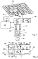
- FIG. 5 shows an induction hob with a matrix of inductors 30 and a control unit 32 which can detect a cookware element 34 placed on the hob and determine the size and shape of the bottom of the cookware element 34 or several cookware elements.
- the control unit 32 summarizes a plurality of inductors 30 to form a flexibly definable heating zone 36.
- a user can set a power level for the heating zone 36 or for a plurality of heating zones 36.
- the control unit 32 interconnects a plurality of inverters 10 of a power supply unit 40 with the inducers 30 of the heating zone 36 in such a way that the inducers 30 of the heating zone 36 couple a total heating power dependent on the set power level into the cookware element 34.
- the inverters 10 or an inverter 10 generate a high-frequency alternating current with a frequency in the order of 50-100 kHz, which flows through the inductors 30 and generates a magnetic field which changes with the same frequency.
- the magnetic field in turn, generates alternating currents in the ferromagnetic bottom of the cookware element 34, thereby heating that bottom.
- the power supply unit 40 comprises a DC voltage source 12 which comprises a rectifier 42 and a filter circuit 44.
- the rectifier 42 is connected to a phase of a household power network 46. Even if in Fig. 1 only one power supply unit 40 is shown, the hob is fed in practice by two power supply units, which are connected to two phases of the household electricity network 46.
- a likewise controlled by the control unit 32 circuitry 48 is provided, can be made and separated via the flexibly configurable connections between the inverters 10 and the inductors 30.
- Fig. 2 shows a circuit with an inverter 10, the two semiconductor switches 14, 16 includes.
- Each of the semiconductor switches 14, 16 consists of a transistor 50, in particular an insulated gate bipolar transistor (IGBT) and a diode 52.
- IGBT insulated gate bipolar transistor
- the inverter 10 with the two semiconductor switches 14, 16 is constructed in a half-bridge topology.
- An upper contact point 54 is connected to a positive output of the DC voltage source 12, and a lower contact point 56 of the circuit is connected to the ground potential.
- each of the damping assemblies 18, 20 comprises two capacitors 28a, 28b.
- a first capacitor 28a is hardwired to the corresponding semiconductor switch 14, 16.
- the two capacitors 28a of the upper and lower semiconductor switches 14, 16 are each connected to a center of the inverter 10, to which the inductor 30 is also connected.
- Each of the damping arrangements 18, 20 additionally comprises a further capacitor 28b.
- the two capacitors 28b are connected in common with an input of a switching element 26, which may be formed, for example, as an electromechanical relay. By closing the switching element 26, the two capacitors 28b can also be connected to the center of the inverter 10, so that the capacitors 28b are connected in parallel with the corresponding semiconductor switch 14, 16.
- the switching element 26 therefore forms, in interaction with the capacitors 28a, 28b, a means 22 for varying a damping constant of the damping arrangements 18, 20.
- By closing the switching element 26, the damping constants of both damping arrangements 18, 20 are changed simultaneously in the same way.
- the capacitors 28a, 28b together form a flexibly configurable snubber capacitor system 24.
- the control unit 32 ( Fig. 1 ) can control the switching element 26 via a control line, not shown here. In order to match the total capacitance of the damping assemblies 18, 20 to a load of the inductor 30, the control unit 32 closes the switching element 26 when a load of the inductor or a power transmitted through the semiconductor switches 14, 16 exceeds a threshold.
- Fig. 3 shows a circuit with three pairs of capacitors 28a, 28b, 28c, wherein each part of the pair is associated with one of the semiconductor switches 14, 16 and one of the damping assemblies 18, 20.
- the capacitors 28a are hardwired to the semiconductor switches 14, 16, and the capacitors 28b and 28c can be switched on or off by switching elements 26a, 26b, respectively.
- the control unit 32 can thereby choose between three possible values of the total capacitance of the damping arrangements 18, 20, between the capacitance of the capacitors 28a, between the sum of the capacitances of the capacitors 28a and 28b and between the sum of the capacitances of all three capacitors 28a, 28b, 28c.
- the capacitances of the capacitors 28b and 28c have the same value, so that the total capacity of the damping capacitor system can be increased starting from a basic value in two stages with the same distance.
- Fig. 4 shows a further alternative embodiment of the invention, in the switching elements 26a, 26b for connecting capacitors 28b, 28c of the damping capacitor system 24 not as in the embodiment after Fig. 3 are connected in series in series, but are connected in parallel with the center of the inverter 10.
- the capacitors 28b, 28c preferably have different capacitances, so that a different total capacitance can be achieved by closing the switching element 26a when the switching element 26b is open than by closing the switching element 26b when the switching element 26a is open. Altogether four different values of the total capacity are adjustable.
- the control unit 32 can prevent leakage during operation.
- the total capacitance, and hence the attenuation constant, of the attenuator assemblies 18, 20 can be matched to the load, such that substantial ringing of the resonant circuits formed by the resonant capacitors 58 and the inductor 10 and discharge of oversized snubber capacitors of one attenuator assembly through the transistor 50 of another Semiconductor circuit can be avoided. At the same time too great inertia of the circuit can be avoided by an over-dimensioned at low power attenuation capacitor.
- Fig. 5 shows power losses in an exemplary embodiment.
- the power losses are composed of power losses, which are represented by a horizontal hatching and switching losses, which are represented by a vertical hatching together.
- Fig. 5 left column shows the losses at a comparatively high power with open switching element 26 in the embodiment according to Fig. 2
- Fig. 5 right column shows the losses at the same power with closed switching element 26 and switched capacitors 28b. It can be seen that the switching losses can be significantly reduced.
- inverter 56 contact point 12
- DC voltage source 58 Resonant capacitor 14
- Semiconductor switches 60 resistance Semiconductor switches 18 damping arrangement 20 damping arrangement 22 medium 24
- Snubber capacitor-system 26 switching element 28a capacitor 28b capacitor 28c capacitor 30 inductor 32
- control unit 34 Cookware element 36 heating zone 38
- Power supply unit 42 rectifier 44 Filter circuit 46 Household power grid 48 circuitry 50 transistor 52 diode 54 contact point
Landscapes
- Physics & Mathematics (AREA)
- Electromagnetism (AREA)
- Induction Heating Cooking Devices (AREA)
- Inverter Devices (AREA)
Claims (7)
- Plaque de cuisson à induction munie d'au moins un onduleur (10) qui comprend au moins deux commutateurs à semi-conducteur (14, 16) raccordés à différents pôles d'une source de tension continue (12), et au moins deux agencements d'atténuation (18, 20) qui sont respectivement disposés parallèlement à l'un des commutateurs à semi-conducteur (14, 16), et munie d'au moins un moyen (22) de réglage d'une constante d'atténuation d'au moins un des agencements d'atténuation (18, 20),
caractérisée en ce que
le moyen (22) est conçu pour la modification simultanée des constantes d'atténuation des agencements d'atténuation (18, 20) des deux commutateurs à semi-conducteur (14, 16). - Plaque de cuisson à induction selon la revendication 1, caractérisée en ce que l'agencement d'atténuation (18, 20) comprend au moins un système de condensateurs d'atténuation (24), le moyen (22) étant conçu pour le réglage d'une capacité totale du système de condensateurs d'atténuation (24).
- Plaque de cuisson à induction selon l'une quelconque des revendications précédentes, caractérisée en ce que l'agencement d'atténuation (18, 20) comprend plusieurs éléments de commutation (26) et plusieurs condensateurs (28) qui sont respectivement connectables par la fermeture d'un élément de commutation (26)
- Plaque de cuisson à induction selon la revendication 3, caractérisée en ce que les condensateurs (28) ont différentes capacités et sont connectables indépendamment les uns des autres.
- Plaque de cuisson à induction selon l'une quelconque des revendications précédentes, caractérisée en ce que l'appareil ménager est une plaque de cuisson à induction et en ce que l'onduleur (10) génère un courant de chauffage pour alimenter des inducteurs (30).
- Plaque de cuisson à induction selon l'une quelconque des revendications précédentes, caractérisée par une unité de commande (32) qui est conçue pour régler la capacité totale en fonction d'une puissance théorique transmise par l'intermédiaire des commutateurs à semi-conducteur (14, 16).
- Plaque de cuisson à induction selon la revendication 6, caractérisée en ce que l'unité de commande (32) augmente la capacité totale par échelons lorsque la puissance théorique ou un courant théorique dépasse une valeur seuil.
Applications Claiming Priority (2)
| Application Number | Priority Date | Filing Date | Title |
|---|---|---|---|
| ES200803710A ES2354093B1 (es) | 2008-12-19 | 2008-12-19 | Aparato domestico con al menos un inversor. |
| PCT/EP2009/066469 WO2010069789A1 (fr) | 2008-12-19 | 2009-12-07 | Appareil ménager comprenant au moins un onduleur |
Publications (2)
| Publication Number | Publication Date |
|---|---|
| EP2380394A1 EP2380394A1 (fr) | 2011-10-26 |
| EP2380394B1 true EP2380394B1 (fr) | 2016-07-27 |
Family
ID=41683325
Family Applications (1)
| Application Number | Title | Priority Date | Filing Date |
|---|---|---|---|
| EP09796993.5A Active EP2380394B1 (fr) | 2008-12-19 | 2009-12-07 | Plaque de cuisson à induction comprenant au moins un onduleur |
Country Status (3)
| Country | Link |
|---|---|
| EP (1) | EP2380394B1 (fr) |
| ES (2) | ES2354093B1 (fr) |
| WO (1) | WO2010069789A1 (fr) |
Cited By (1)
| Publication number | Priority date | Publication date | Assignee | Title |
|---|---|---|---|---|
| WO2022233654A1 (fr) * | 2021-05-03 | 2022-11-10 | BSH Hausgeräte GmbH | Dispositif d'alimentation en énergie par induction |
Families Citing this family (1)
| Publication number | Priority date | Publication date | Assignee | Title |
|---|---|---|---|---|
| ES2408863R1 (es) * | 2011-10-26 | 2013-08-06 | Bsh Electrodomesticos Espana | Dispositivo de calentamiento por inducción dotado de elementos condensadores |
Family Cites Families (5)
| Publication number | Priority date | Publication date | Assignee | Title |
|---|---|---|---|---|
| JP2006114320A (ja) * | 2004-10-14 | 2006-04-27 | Mitsubishi Electric Corp | 誘導加熱装置及び誘導加熱調理器 |
| JP4512525B2 (ja) * | 2005-07-01 | 2010-07-28 | 日立アプライアンス株式会社 | 誘導加熱調理器 |
| JP4652983B2 (ja) * | 2006-01-18 | 2011-03-16 | 日立アプライアンス株式会社 | 誘導加熱装置 |
| JP4868952B2 (ja) * | 2006-06-16 | 2012-02-01 | 三菱電機株式会社 | 誘導加熱調理器 |
| JP4909662B2 (ja) * | 2006-07-12 | 2012-04-04 | 日立アプライアンス株式会社 | 電磁誘導加熱装置 |
-
2008
- 2008-12-19 ES ES200803710A patent/ES2354093B1/es not_active Withdrawn - After Issue
-
2009
- 2009-12-07 ES ES09796993.5T patent/ES2586465T3/es active Active
- 2009-12-07 EP EP09796993.5A patent/EP2380394B1/fr active Active
- 2009-12-07 WO PCT/EP2009/066469 patent/WO2010069789A1/fr not_active Ceased
Cited By (1)
| Publication number | Priority date | Publication date | Assignee | Title |
|---|---|---|---|---|
| WO2022233654A1 (fr) * | 2021-05-03 | 2022-11-10 | BSH Hausgeräte GmbH | Dispositif d'alimentation en énergie par induction |
Also Published As
| Publication number | Publication date |
|---|---|
| ES2354093B1 (es) | 2012-01-26 |
| ES2586465T3 (es) | 2016-10-14 |
| ES2354093A1 (es) | 2011-03-10 |
| WO2010069789A1 (fr) | 2010-06-24 |
| EP2380394A1 (fr) | 2011-10-26 |
Similar Documents
| Publication | Publication Date | Title |
|---|---|---|
| EP2389787B1 (fr) | Plaque de cuisson comportant au moins une zone de chauffe composée de plusieurs éléments de chauffe | |
| EP2564666B1 (fr) | Ensemble table de cuisson | |
| EP1931177B1 (fr) | Circuit de dispositif de chauffage | |
| EP2586271B1 (fr) | Ensemble table de cuisson | |
| EP2494846B1 (fr) | Plaque de cuisson à au moins deux résistances, et dispositif électronique de puissance | |
| DE2535637A1 (de) | Induktionsheizvorrichtung | |
| EP2638777B1 (fr) | Dispositif chauffant | |
| EP2506663B1 (fr) | Dispositif d'appareil de cuisson | |
| EP2469970B1 (fr) | Dispositif d'appareil de cuisson | |
| EP2744299A1 (fr) | Dispositif domestique de chauffage par induction | |
| EP2384083A1 (fr) | Agencement de commutation pour un appareil de cuisson à induction, procédé de fonctionnement d'un agencement de commutation et appareil de cuisson à induction | |
| EP3556179B1 (fr) | Dispositif pour appareil ménager | |
| EP3556181B1 (fr) | Appareil électroménager | |
| EP2506673B1 (fr) | Plaque de cuisson a induction | |
| EP2380394B1 (fr) | Plaque de cuisson à induction comprenant au moins un onduleur | |
| EP3556180B1 (fr) | Appareil électroménager | |
| DE19841759C2 (de) | Elektromagnetisches Kochgerät | |
| EP2692202B1 (fr) | Dispositif de chauffage par induction | |
| EP2515608B1 (fr) | Dispositif d'appareil ménager | |
| EP2214454B1 (fr) | Champ de cuisson à induction doté de plusieurs inducteurs | |
| EP2506670B1 (fr) | Dispositif de chauffage à induction | |
| EP2506667B1 (fr) | Dispositif de chauffage à induction | |
| EP2550841B1 (fr) | Ensemble plaque de cuisson | |
| EP2706817B1 (fr) | Plaque de cuisson | |
| DE102012206940A1 (de) | Induktionsheizvorrichtung |
Legal Events
| Date | Code | Title | Description |
|---|---|---|---|
| PUAI | Public reference made under article 153(3) epc to a published international application that has entered the european phase |
Free format text: ORIGINAL CODE: 0009012 |
|
| 17P | Request for examination filed |
Effective date: 20110719 |
|
| AK | Designated contracting states |
Kind code of ref document: A1 Designated state(s): AT BE BG CH CY CZ DE DK EE ES FI FR GB GR HR HU IE IS IT LI LT LU LV MC MK MT NL NO PL PT RO SE SI SK SM TR |
|
| DAX | Request for extension of the european patent (deleted) | ||
| RAP1 | Party data changed (applicant data changed or rights of an application transferred) |
Owner name: BSH HAUSGERAETE GMBH |
|
| 17Q | First examination report despatched |
Effective date: 20150608 |
|
| GRAP | Despatch of communication of intention to grant a patent |
Free format text: ORIGINAL CODE: EPIDOSNIGR1 |
|
| INTG | Intention to grant announced |
Effective date: 20160310 |
|
| GRAS | Grant fee paid |
Free format text: ORIGINAL CODE: EPIDOSNIGR3 |
|
| GRAA | (expected) grant |
Free format text: ORIGINAL CODE: 0009210 |
|
| AK | Designated contracting states |
Kind code of ref document: B1 Designated state(s): AT BE BG CH CY CZ DE DK EE ES FI FR GB GR HR HU IE IS IT LI LT LU LV MC MK MT NL NO PL PT RO SE SI SK SM TR |
|
| REG | Reference to a national code |
Ref country code: GB Ref legal event code: FG4D Free format text: NOT ENGLISH |
|
| REG | Reference to a national code |
Ref country code: CH Ref legal event code: EP |
|
| REG | Reference to a national code |
Ref country code: AT Ref legal event code: REF Ref document number: 816709 Country of ref document: AT Kind code of ref document: T Effective date: 20160815 |
|
| REG | Reference to a national code |
Ref country code: IE Ref legal event code: FG4D Free format text: LANGUAGE OF EP DOCUMENT: GERMAN |
|
| REG | Reference to a national code |
Ref country code: DE Ref legal event code: R096 Ref document number: 502009012891 Country of ref document: DE |
|
| REG | Reference to a national code |
Ref country code: ES Ref legal event code: FG2A Ref document number: 2586465 Country of ref document: ES Kind code of ref document: T3 Effective date: 20161014 |
|
| REG | Reference to a national code |
Ref country code: LT Ref legal event code: MG4D |
|
| REG | Reference to a national code |
Ref country code: NL Ref legal event code: MP Effective date: 20160727 |
|
| REG | Reference to a national code |
Ref country code: FR Ref legal event code: PLFP Year of fee payment: 8 |
|
| PG25 | Lapsed in a contracting state [announced via postgrant information from national office to epo] |
Ref country code: IS Free format text: LAPSE BECAUSE OF FAILURE TO SUBMIT A TRANSLATION OF THE DESCRIPTION OR TO PAY THE FEE WITHIN THE PRESCRIBED TIME-LIMIT Effective date: 20161127 Ref country code: HR Free format text: LAPSE BECAUSE OF FAILURE TO SUBMIT A TRANSLATION OF THE DESCRIPTION OR TO PAY THE FEE WITHIN THE PRESCRIBED TIME-LIMIT Effective date: 20160727 Ref country code: NO Free format text: LAPSE BECAUSE OF FAILURE TO SUBMIT A TRANSLATION OF THE DESCRIPTION OR TO PAY THE FEE WITHIN THE PRESCRIBED TIME-LIMIT Effective date: 20161027 Ref country code: NL Free format text: LAPSE BECAUSE OF FAILURE TO SUBMIT A TRANSLATION OF THE DESCRIPTION OR TO PAY THE FEE WITHIN THE PRESCRIBED TIME-LIMIT Effective date: 20160727 Ref country code: LT Free format text: LAPSE BECAUSE OF FAILURE TO SUBMIT A TRANSLATION OF THE DESCRIPTION OR TO PAY THE FEE WITHIN THE PRESCRIBED TIME-LIMIT Effective date: 20160727 Ref country code: FI Free format text: LAPSE BECAUSE OF FAILURE TO SUBMIT A TRANSLATION OF THE DESCRIPTION OR TO PAY THE FEE WITHIN THE PRESCRIBED TIME-LIMIT Effective date: 20160727 |
|
| PG25 | Lapsed in a contracting state [announced via postgrant information from national office to epo] |
Ref country code: PT Free format text: LAPSE BECAUSE OF FAILURE TO SUBMIT A TRANSLATION OF THE DESCRIPTION OR TO PAY THE FEE WITHIN THE PRESCRIBED TIME-LIMIT Effective date: 20161128 Ref country code: LV Free format text: LAPSE BECAUSE OF FAILURE TO SUBMIT A TRANSLATION OF THE DESCRIPTION OR TO PAY THE FEE WITHIN THE PRESCRIBED TIME-LIMIT Effective date: 20160727 Ref country code: PL Free format text: LAPSE BECAUSE OF FAILURE TO SUBMIT A TRANSLATION OF THE DESCRIPTION OR TO PAY THE FEE WITHIN THE PRESCRIBED TIME-LIMIT Effective date: 20160727 Ref country code: SE Free format text: LAPSE BECAUSE OF FAILURE TO SUBMIT A TRANSLATION OF THE DESCRIPTION OR TO PAY THE FEE WITHIN THE PRESCRIBED TIME-LIMIT Effective date: 20160727 |
|
| PG25 | Lapsed in a contracting state [announced via postgrant information from national office to epo] |
Ref country code: RO Free format text: LAPSE BECAUSE OF FAILURE TO SUBMIT A TRANSLATION OF THE DESCRIPTION OR TO PAY THE FEE WITHIN THE PRESCRIBED TIME-LIMIT Effective date: 20160727 Ref country code: EE Free format text: LAPSE BECAUSE OF FAILURE TO SUBMIT A TRANSLATION OF THE DESCRIPTION OR TO PAY THE FEE WITHIN THE PRESCRIBED TIME-LIMIT Effective date: 20160727 |
|
| REG | Reference to a national code |
Ref country code: DE Ref legal event code: R097 Ref document number: 502009012891 Country of ref document: DE |
|
| PG25 | Lapsed in a contracting state [announced via postgrant information from national office to epo] |
Ref country code: SM Free format text: LAPSE BECAUSE OF FAILURE TO SUBMIT A TRANSLATION OF THE DESCRIPTION OR TO PAY THE FEE WITHIN THE PRESCRIBED TIME-LIMIT Effective date: 20160727 Ref country code: DK Free format text: LAPSE BECAUSE OF FAILURE TO SUBMIT A TRANSLATION OF THE DESCRIPTION OR TO PAY THE FEE WITHIN THE PRESCRIBED TIME-LIMIT Effective date: 20160727 Ref country code: BE Free format text: LAPSE BECAUSE OF NON-PAYMENT OF DUE FEES Effective date: 20161231 Ref country code: BG Free format text: LAPSE BECAUSE OF FAILURE TO SUBMIT A TRANSLATION OF THE DESCRIPTION OR TO PAY THE FEE WITHIN THE PRESCRIBED TIME-LIMIT Effective date: 20161027 Ref country code: SK Free format text: LAPSE BECAUSE OF FAILURE TO SUBMIT A TRANSLATION OF THE DESCRIPTION OR TO PAY THE FEE WITHIN THE PRESCRIBED TIME-LIMIT Effective date: 20160727 Ref country code: CZ Free format text: LAPSE BECAUSE OF FAILURE TO SUBMIT A TRANSLATION OF THE DESCRIPTION OR TO PAY THE FEE WITHIN THE PRESCRIBED TIME-LIMIT Effective date: 20160727 |
|
| PLBE | No opposition filed within time limit |
Free format text: ORIGINAL CODE: 0009261 |
|
| STAA | Information on the status of an ep patent application or granted ep patent |
Free format text: STATUS: NO OPPOSITION FILED WITHIN TIME LIMIT |
|
| 26N | No opposition filed |
Effective date: 20170502 |
|
| REG | Reference to a national code |
Ref country code: CH Ref legal event code: PL |
|
| PG25 | Lapsed in a contracting state [announced via postgrant information from national office to epo] |
Ref country code: SI Free format text: LAPSE BECAUSE OF FAILURE TO SUBMIT A TRANSLATION OF THE DESCRIPTION OR TO PAY THE FEE WITHIN THE PRESCRIBED TIME-LIMIT Effective date: 20160727 |
|
| PG25 | Lapsed in a contracting state [announced via postgrant information from national office to epo] |
Ref country code: MC Free format text: LAPSE BECAUSE OF FAILURE TO SUBMIT A TRANSLATION OF THE DESCRIPTION OR TO PAY THE FEE WITHIN THE PRESCRIBED TIME-LIMIT Effective date: 20160727 |
|
| REG | Reference to a national code |
Ref country code: IE Ref legal event code: MM4A |
|
| PG25 | Lapsed in a contracting state [announced via postgrant information from national office to epo] |
Ref country code: LI Free format text: LAPSE BECAUSE OF NON-PAYMENT OF DUE FEES Effective date: 20161231 Ref country code: LU Free format text: LAPSE BECAUSE OF NON-PAYMENT OF DUE FEES Effective date: 20161207 Ref country code: CH Free format text: LAPSE BECAUSE OF NON-PAYMENT OF DUE FEES Effective date: 20161231 |
|
| PG25 | Lapsed in a contracting state [announced via postgrant information from national office to epo] |
Ref country code: IE Free format text: LAPSE BECAUSE OF NON-PAYMENT OF DUE FEES Effective date: 20161207 |
|
| REG | Reference to a national code |
Ref country code: FR Ref legal event code: PLFP Year of fee payment: 9 |
|
| REG | Reference to a national code |
Ref country code: BE Ref legal event code: MM Effective date: 20161231 |
|
| REG | Reference to a national code |
Ref country code: AT Ref legal event code: MM01 Ref document number: 816709 Country of ref document: AT Kind code of ref document: T Effective date: 20161207 |
|
| PG25 | Lapsed in a contracting state [announced via postgrant information from national office to epo] |
Ref country code: HU Free format text: LAPSE BECAUSE OF FAILURE TO SUBMIT A TRANSLATION OF THE DESCRIPTION OR TO PAY THE FEE WITHIN THE PRESCRIBED TIME-LIMIT; INVALID AB INITIO Effective date: 20091207 Ref country code: CY Free format text: LAPSE BECAUSE OF FAILURE TO SUBMIT A TRANSLATION OF THE DESCRIPTION OR TO PAY THE FEE WITHIN THE PRESCRIBED TIME-LIMIT Effective date: 20160727 Ref country code: AT Free format text: LAPSE BECAUSE OF NON-PAYMENT OF DUE FEES Effective date: 20161207 |
|
| PG25 | Lapsed in a contracting state [announced via postgrant information from national office to epo] |
Ref country code: MK Free format text: LAPSE BECAUSE OF FAILURE TO SUBMIT A TRANSLATION OF THE DESCRIPTION OR TO PAY THE FEE WITHIN THE PRESCRIBED TIME-LIMIT Effective date: 20160727 Ref country code: TR Free format text: LAPSE BECAUSE OF FAILURE TO SUBMIT A TRANSLATION OF THE DESCRIPTION OR TO PAY THE FEE WITHIN THE PRESCRIBED TIME-LIMIT Effective date: 20160727 Ref country code: GR Free format text: LAPSE BECAUSE OF FAILURE TO SUBMIT A TRANSLATION OF THE DESCRIPTION OR TO PAY THE FEE WITHIN THE PRESCRIBED TIME-LIMIT Effective date: 20160727 |
|
| PG25 | Lapsed in a contracting state [announced via postgrant information from national office to epo] |
Ref country code: MT Free format text: LAPSE BECAUSE OF FAILURE TO SUBMIT A TRANSLATION OF THE DESCRIPTION OR TO PAY THE FEE WITHIN THE PRESCRIBED TIME-LIMIT Effective date: 20160727 |
|
| PGFP | Annual fee paid to national office [announced via postgrant information from national office to epo] |
Ref country code: GB Payment date: 20251218 Year of fee payment: 17 |
|
| PGFP | Annual fee paid to national office [announced via postgrant information from national office to epo] |
Ref country code: FR Payment date: 20251217 Year of fee payment: 17 |
|
| PGFP | Annual fee paid to national office [announced via postgrant information from national office to epo] |
Ref country code: ES Payment date: 20260119 Year of fee payment: 17 |
|
| PGFP | Annual fee paid to national office [announced via postgrant information from national office to epo] |
Ref country code: DE Payment date: 20251231 Year of fee payment: 17 |
|
| PGFP | Annual fee paid to national office [announced via postgrant information from national office to epo] |
Ref country code: IT Payment date: 20251231 Year of fee payment: 17 |