EP2381465A1 - Werkzeugspitzen-Interface für ein Komponentenhandhabungswerkzeug - Google Patents
Werkzeugspitzen-Interface für ein Komponentenhandhabungswerkzeug Download PDFInfo
- Publication number
- EP2381465A1 EP2381465A1 EP10160809A EP10160809A EP2381465A1 EP 2381465 A1 EP2381465 A1 EP 2381465A1 EP 10160809 A EP10160809 A EP 10160809A EP 10160809 A EP10160809 A EP 10160809A EP 2381465 A1 EP2381465 A1 EP 2381465A1
- Authority
- EP
- European Patent Office
- Prior art keywords
- tool tip
- interface
- tool
- handling
- die
- Prior art date
- Legal status (The legal status is an assumption and is not a legal conclusion. Google has not performed a legal analysis and makes no representation as to the accuracy of the status listed.)
- Withdrawn
Links
Images



Classifications
-
- H—ELECTRICITY
- H10—SEMICONDUCTOR DEVICES; ELECTRIC SOLID-STATE DEVICES NOT OTHERWISE PROVIDED FOR
- H10P—GENERIC PROCESSES OR APPARATUS FOR THE MANUFACTURE OR TREATMENT OF DEVICES COVERED BY CLASS H10
- H10P72/00—Handling or holding of wafers, substrates or devices during manufacture or treatment thereof
- H10P72/70—Handling or holding of wafers, substrates or devices during manufacture or treatment thereof for supporting or gripping
- H10P72/78—Handling or holding of wafers, substrates or devices during manufacture or treatment thereof for supporting or gripping using vacuum or suction, e.g. Bernoulli chucks
-
- H—ELECTRICITY
- H10—SEMICONDUCTOR DEVICES; ELECTRIC SOLID-STATE DEVICES NOT OTHERWISE PROVIDED FOR
- H10P—GENERIC PROCESSES OR APPARATUS FOR THE MANUFACTURE OR TREATMENT OF DEVICES COVERED BY CLASS H10
- H10P72/00—Handling or holding of wafers, substrates or devices during manufacture or treatment thereof
- H10P72/04—Apparatus for manufacture or treatment
- H10P72/0446—Apparatus for mounting on conductive members, e.g. leadframes or conductors on insulating substrates
Definitions
- the present invention pertains to the field of automation technology. It relates to a tool tip interface, in particular a shank, for use with a handling unit, in particular for a die bonder, configured to handle a planar object, in particular a semiconductor die, in accordance with the preamble of the independent patent claim.
- the semiconductor chips are generally provided on a carrier tape, which generally contains a whole semiconductor wafer that has been cut into small chips, a process frequently referred to as dicing.
- the semiconductor chips are thus commonly referred to as dies.
- the carrier tape is often the same tape that supported the wafer during dicing, often referred to as dicing tape. Die thicknesses of down to 25 ⁇ m are common today, and there is an ongoing trend to decrease thicknesses even further.
- Die bonders pick a single die from the carrier tape and place and subsequently attach the picked die onto a substrate or onto another die. In most situations, the die is attached permanently, but configurations where dies are only attached temporarily also exist. Often, a temporary attachment is subsequently turned into a permanent one by an additional heating and/or pressing process. Often, thin dies come with a wafer backside lamination (WBL) or film or flow over wire (FOW) lamination, i.e. an adhesive film which is applied to an unstructured side of the wafer or die.
- WBL wafer backside lamination
- FOW flow over wire
- a process of thinning wafers, applying an adhesive film to the wafers, mounting the wafers to a carrier tape and frame, and dicing them into individual chips is usually referred to as wafer preparation.
- the lamination which allows for the dies to be attached due to its adhesive properties, may be provided either between the carrier tape and the wafer, or on a surface of the wafer facing away from the carrier tape.
- the fabrication of very thin wafers and the corresponding dies is very expensive as compared to standard thickness wafers without lamination.
- Picking and placing or attaching may be carried out by a single die handling unit in the die bonder.
- a plurality of die handling units can be present:
- picking takes place from a so called wafer table, and is assisted by a die ejector 91.
- the die ejector 91 facilitates the removal of the die 5 from the carrier tape 4, e.g. by pushing the die 5 against a first die handling unit called pick unit 92 - from underneath the carrier tape 4.
- the pick unit 92 subsequently picks the die 5 from the carrier tape 4 in a pick process.
- the die 5 is then handed over to a second die handling unit, also referred to as place unit 94.
- the place unit 94 places the die 5 onto a mounting location, where it is attached.
- at least one third die handling unit - a so called transfer unit 93 - is provided to hand the die 5 from the pick unit 92 to the place unit 94.
- An example is given in WO 07118511 A1 which is hereby incorporated by reference in its entirety.
- a die 5 may be attached to mounting location on a mounting surface of a substrate 6, e.g. a leadframe, printed circuit board, multilayer board etc., or of another die, which itself may be have been attached in the same way.
- a plurality of cameras 40, 41, 42, 44 is normally present for monitoring and/or measuring purposes.
- Pick, place, and - if present - transfer unit each comprise a handling tool, which in turn comprises a work surface to which the die 5 becomes temporarily attached during handling, i.e. delivery to the target location of the respective handling unit.
- Temporary attachment is most frequently achieved by means of vacuum suction.
- the work surface is frequently formed on a region of a soft elastic material that acts as or forms part of a tool tip. Often, this is a rubber or silicone layer formed on an otherwise metallic handling tool. The presence of such a region of a soft elastic material helps to avoid chip damage, e.g.
- the tool tip comprises an essentially flat material section in which a plurality of through holes having first openings in the work surface are provided; and a back side from which vacuum may be supplied to the through holes.
- the tool tip is formed exclusively from the soft elastic material and is detachably mounted to a tool tip interface, which is often provided in the form of a so-called shank.
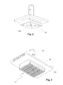
- Fig. 2 shows a perspective view of a prior art shank.
- the tool tip comprises an essentially flat material section in which a plurality of through holes having openings in the work surface are provided; and a back side from which vacuum may be supplied to the through holes.
- Known shanks consist of an essentially flat plate on a first side of which a hollow shaft is provided.
- a vacuum may be fed through the shaft to one or more vacuum channels 10 provided on a bottom side of the flat plate.
- the vacuum channels 10 are designed to cover as little of a surface of the bottom side as possible. This is achieved by making them as narrow as possible while still allowing for sufficient vacuum flow to securely fix dies 5 to the work surface. Also, they are designed to have minimum overall length, which often results in a star shaped arrangement around a small, central vacuum hole located in the center of the bottom side of the flat plate.
- a flat bearing surface 100 for the tool tip is formed that covers a major part of the bottom side of the flat plate, typically more than 90% or even 95%.
- a heating element for heating the die 5 as required for many die bonding processes is often provided in the die handling unit and thus relatively far from the die 5 for cost efficiency and to avoid mounting and contact problems etc. that arise from a necessity of frequent exchange of shanks.
- a tool tip interface for use with a handling tool configured to handle a planar object, in particular a semiconductor die, comprises: a machine side interface which comprises a vacuum supply connection; a tip side interface having a bottom side on which a support surface for a tool tip (3) is formed and on which one or more depressions are formed so that the one or more depressions define support surface portions which are at least partially surrounded by depressed regions, wherein support surface portions and depressed regions are uniformly distributed over at least a central region of the bottom side of the tip side interface.
- Fig. 3 shows a perspective view of a tool tip interface 11 in accordance with an exemplary embodiment of the present invention.
- the tool tip interface 11 is formed as an integrated part of a shank, which further comprises a hollow shaft 12 by means of which the shank my be mounted to a die handling unit, and which acts as machine side interface of the tool tip interface 11.
- a support surface was formed by working an initially planar surface so that a grid shaped depression results, e.g. by means of engraving, milling, embossing, electro-abrasion, etc.
- Fig. 4 shows a top view of the bottom side of the tool tip interface 11. In the example shown in Figs.
- the grid shaped depression consists of 19 grooves extending in a first direction, and 3 groves extending in a second direction perpendicular to the first direction.
- the grid shaped depression is formed in a central region of the bottom side of the tool tip interface 11, with grid dimensions chosen so that only a narrow peripheral region 21 of the bottom side remains where no grooves are formed.
- Isolated ridges 22 have rectangular planar surfaces which are surrounded by grooves on all sides.
- Contiguous ridges 23 are located adjacent to the peripheral region 21, and are surrounded by grooves on three sides.
- the contiguous ridges 23 also have planar surfaces.
- the planar surfaces of both the isolated and contiguous ridges 22, 23 form support surface portions of a planar central support surface for a tool tip 3, with all the support surface portions lying in one plane.
- a surface of the narrow peripheral region 21 is also located in that plane, and acts as a peripheral support surface. In the central region of the bottom side of the tool tip interface 11, both support surface portions and depressed regions are thus uniformly distributed.
- the narrow peripheral region has a width w P of approximately w P ⁇ 2 w R .
- a carrier plate 15 for a heating element e.g. a thin film of Al 2 O 3 with electrical connections for applying a voltage
- the carrier plate 15 and the bottom side of the tool tip interface 11 are made of a copper alloy to allow for efficient heating of a die attached to the work surface. By thus providing the heating element on the shank rather than within the handling unit, efficient heating with rapid changes in die temperature is possible.
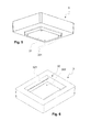
- Figs. 5 and 6 show perspective views of a tool tip 3 for use in connection with a tool tip interface 11 in accordance with the present invention.
- the tool tip 3 is made of an elastomeric material, in particular a rubber, preferably a silicone rubber, and is essentially box-shaped.
- a rectangular work surface 31 is formed on a front side of the tool tip 3.
- a recession 32 provided on a back side of the tool tip 3 allows for mounting the tool tip 3 to the tool tip interface 11 by putting the tool tip 3 over the bottom side of the tool tip interface 11.
- the recession 32 preferably has a flat bottom, which will thus come in tight contact with the support surface of the tool tip interface 11.
- Lateral indentations 110 are provided near the bottom side of the tool tip interface 11, and may interact with protrusions 321 formed on an upper end of one or more side walls of the recession 32 to allow for tightly fixing the tool tip 3 to the tool tip interface 11.
- the grooves formed on the bottom side of the tool tip interface 11 serve as first vacuum ducts and are connectable to a vacuum supply through the hollow shaft 12 of the shank, which is configured to be used as a vacuum supply connection.
- a plurality of through holes is provided in the tool tip 3 to act as second vacuum ducts.
- the through holes form first through hole openings 301 and second through hole openings 302 on the front and back side of the tool tip 3, respectively.
- the second through hole openings 302 have a diameter d 2 which equals - at least approximately - twice the width w R of the ridges 22, 23 of the tool tip interface 11.
- each of the second through hole openings 302 is configured to satisfy the relation 1.2 w R ⁇ d 2 ⁇ 3.5 w R , preferably 1.5 w R ⁇ d 2 ⁇ 2.5 w R .
- the second through hole openings 302 may be provided at arbitrary locations on the flat bottom of the recession 32. As long as w R ⁇ d 2 is fulfilled, it is always guaranteed that the respective second through hole opening 302 may not be completely obstructed by a ridge 22, 23 upon which it may come to rest when the tool tip 3 is mounted to the tool tip interface 11. In this way, an unobstructed vacuum flow between the first and second vacuum ducts is ensured.
- through holes having second through hole openings 302 of non-circular shape may also be employed to advantage. In this case, an average width or average cross section length of the second through hole opening 302 needs to be taken for the value of the diameter d 2 in the above relations.
- the peripheral support surface area A s,p is preferably chosen to be significantly smaller than a sum A s,c + A d of the central support surface area A s,c and the cross section area A d of the depressed regions.
- 3 A s,p ⁇ A s,c + A d holds, preferably 5 A s,p ⁇ A s,c + A d ; and/or 2 A s,p ⁇ A s,c and 2 A s,p ⁇ A d is simultaneously fulfilled.
- Preferably 0.5 A s,c ⁇ A d ⁇ 2 A s,c is also fulfilled, preferably 0.75 A s,c ⁇ A d ⁇ 1.33A s,c or A d ⁇ A s,c .
- tool tips 3 having varying work surface dimensions may be used on one and the same tool tip interface 11.
- a handling tool range is thus obtained, allowing for a handling unit to be quickly and easily adapted to handling of dies with varying dimensions by simply exchanging the tool tip 3.
- tool tips 3 may have a work surface of significantly smaller dimensions than a bottom side of the tool tip interface 11 and/or the sum A s,c + A d of the central support surface area A s,c and the cross section area A d of the depressed regions of the tool tip interface 11.
- across section of the front side of such tool tips 3 exhibits a step profile.
- a number and/or spatial distribution of the second through hole openings 302 may also be varied. Even the diameter d 2 of the second through hole openings 302 may vary, as long as w R ⁇ d 2 is fulfilled, where advantageously 1.2 w R ⁇ d 2 ⁇ 3.5 w R , preferably 1.5 w R ⁇ d 2 ⁇ 2.5 w R as detailed above.
- identical tool tip interfaces 11 may be used with various die handling units within a die bonder.
- Fig. 7 and 8 show an alternative embodiment of a tool tip interface 11' in accordance with the present invention.
- no isolated ridges exist. Only contiguous ridges 23 are present on the bottom side. Due to a presence of obtuse angles between grooves extending in first and second direction between the contiguous ridges 23 and diagonal grooves connecting the former to the central hole 29, an undisturbed vacuum flow is possible from depressed regions near the peripheral region 21 of the bottom side, allowing for rapid evacuation of the first vacuum ducts when a die is to be fixed to the work surface 31.
- the tool tip interface 11, 11' was formed as an integrated part of a shank, it may advantageously also be formed as a separate entity that may be reversibly attached either to a shank, which may in turn be attached to a die handling unit, or to a die handling unit directly.
- a suitable machine side interface using features known to a person skilled in the art may then allow for rigid mechanical connection, as well as for airtight connection of the vacuum supply connection to a vacuum supply comprised with the die bonder.
- the support surface portions are randomly distributed across the bottom side of the tool tip interface.
- a corresponding support surface can e.g. be obtained by smoothening of a rough surface e.g. by polishing to such an extent that elevations in a surface roughness profile exceeding a given altitude are removed.
- a support surface will result that may be characterized by a maximum distance d max between a point on any of the support surface portions and the nearest depressed region.
- the tool tip interface may then be used with tool tips 3 having second through hole openings 302 at arbitrary locations as long as the diameter d 2 of the second through hole openings 302 is larger than twice the maximum distance d max , i.e. d 2 > 2 d max , where preferably 2.5 d max ⁇ d 2 ⁇ 7 d max , preferably 3 d max ⁇ d 2 ⁇ 5 d max .
- both the grooves and the support surface may also have the shape of a two-dimensional spiral with e.g. circular and/or rectangular windings.
- Each winding of the support surface can then be regarded as a support surface portion, which is surrounded by two windings of the groove.
Landscapes
- Container, Conveyance, Adherence, Positioning, Of Wafer (AREA)
Priority Applications (1)
| Application Number | Priority Date | Filing Date | Title |
|---|---|---|---|
| EP10160809A EP2381465A1 (de) | 2010-04-22 | 2010-04-22 | Werkzeugspitzen-Interface für ein Komponentenhandhabungswerkzeug |
Applications Claiming Priority (1)
| Application Number | Priority Date | Filing Date | Title |
|---|---|---|---|
| EP10160809A EP2381465A1 (de) | 2010-04-22 | 2010-04-22 | Werkzeugspitzen-Interface für ein Komponentenhandhabungswerkzeug |
Publications (1)
| Publication Number | Publication Date |
|---|---|
| EP2381465A1 true EP2381465A1 (de) | 2011-10-26 |
Family
ID=42153790
Family Applications (1)
| Application Number | Title | Priority Date | Filing Date |
|---|---|---|---|
| EP10160809A Withdrawn EP2381465A1 (de) | 2010-04-22 | 2010-04-22 | Werkzeugspitzen-Interface für ein Komponentenhandhabungswerkzeug |
Country Status (1)
| Country | Link |
|---|---|
| EP (1) | EP2381465A1 (de) |
Cited By (1)
| Publication number | Priority date | Publication date | Assignee | Title |
|---|---|---|---|---|
| US20240274461A1 (en) * | 2023-02-15 | 2024-08-15 | Taiwan Semiconductor Manufacturing Company Limited | Bonding tool for providing chip on wafer bond and methods for performing the same |
Citations (7)
| Publication number | Priority date | Publication date | Assignee | Title |
|---|---|---|---|---|
| JPH06177226A (ja) * | 1992-12-03 | 1994-06-24 | Nec Corp | 吸着コレット |
| JP2002134906A (ja) * | 2000-10-20 | 2002-05-10 | Matsushita Electric Ind Co Ltd | 電子部品の熱圧着装置および熱圧着方法 |
| WO2005029574A1 (ja) * | 2003-09-18 | 2005-03-31 | Nec Machinery Corporation | コレット、ダイボンダおよびチップのピックアップ方法 |
| EP1753284A1 (de) * | 2004-05-17 | 2007-02-14 | Matsushita Electric Industrial Co., Ltd. | Teilezuführungs-kopfeinrichtung und teileanbring-kopfeinrichtung |
| WO2007118511A1 (de) | 2006-04-12 | 2007-10-25 | Alphasem Gmbh | Verfahren und vorrichtung zum ablegen von elektronischen bauteilen, insbesondere halbleiterchips auf einem substrat |
| US20080148558A1 (en) * | 2006-12-22 | 2008-06-26 | Samsung Electronics Co., Ltd. | Apparatus for transferring semiconductor chip and method of transferring semiconductor chip using the same |
| JP2008290170A (ja) * | 2007-05-23 | 2008-12-04 | Renesas Technology Corp | 半導体装置の製造方法 |
-
2010
- 2010-04-22 EP EP10160809A patent/EP2381465A1/de not_active Withdrawn
Patent Citations (7)
| Publication number | Priority date | Publication date | Assignee | Title |
|---|---|---|---|---|
| JPH06177226A (ja) * | 1992-12-03 | 1994-06-24 | Nec Corp | 吸着コレット |
| JP2002134906A (ja) * | 2000-10-20 | 2002-05-10 | Matsushita Electric Ind Co Ltd | 電子部品の熱圧着装置および熱圧着方法 |
| WO2005029574A1 (ja) * | 2003-09-18 | 2005-03-31 | Nec Machinery Corporation | コレット、ダイボンダおよびチップのピックアップ方法 |
| EP1753284A1 (de) * | 2004-05-17 | 2007-02-14 | Matsushita Electric Industrial Co., Ltd. | Teilezuführungs-kopfeinrichtung und teileanbring-kopfeinrichtung |
| WO2007118511A1 (de) | 2006-04-12 | 2007-10-25 | Alphasem Gmbh | Verfahren und vorrichtung zum ablegen von elektronischen bauteilen, insbesondere halbleiterchips auf einem substrat |
| US20080148558A1 (en) * | 2006-12-22 | 2008-06-26 | Samsung Electronics Co., Ltd. | Apparatus for transferring semiconductor chip and method of transferring semiconductor chip using the same |
| JP2008290170A (ja) * | 2007-05-23 | 2008-12-04 | Renesas Technology Corp | 半導体装置の製造方法 |
Cited By (1)
| Publication number | Priority date | Publication date | Assignee | Title |
|---|---|---|---|---|
| US20240274461A1 (en) * | 2023-02-15 | 2024-08-15 | Taiwan Semiconductor Manufacturing Company Limited | Bonding tool for providing chip on wafer bond and methods for performing the same |
Similar Documents
| Publication | Publication Date | Title |
|---|---|---|
| US20120168089A1 (en) | Tool for picking a planar object from a supply station | |
| JP6128459B2 (ja) | 金属箔から半導体チップを剥離する方法 | |
| JP5663126B2 (ja) | ワーク搬送方法及びワーク受渡し機構を有する装置 | |
| CN101529577A (zh) | 固定夹具及芯片的拾取方法以及拾取装置 | |
| US20090061596A1 (en) | Expanding tool, expanding method, and manufacturing method of unit elements | |
| JP6967411B2 (ja) | 半導体製造装置、半導体装置の製造方法およびコレット | |
| JP2013172122A (ja) | ダイボンダ | |
| JP2008290170A (ja) | 半導体装置の製造方法 | |
| TWI706499B (zh) | 晶片收容托盤 | |
| US20240021448A1 (en) | Pick-and-place tool and method of manufacturing semiconductor structure | |
| JP2019054209A5 (de) | ||
| JP2011049193A (ja) | 切削装置 | |
| JP2007036143A (ja) | 半導体ウエーハの加工方法 | |
| US20080164646A1 (en) | Workholder for supporting electronic devices | |
| JP3484936B2 (ja) | チップ状部品の取扱方法および装置 | |
| JP4659613B2 (ja) | ワッシャホルダーおよびワッシャ供給源装置 | |
| US20180236639A1 (en) | Support for flexible workpieces | |
| JP4061261B2 (ja) | ダイボンディング用コレット | |
| JP2008270417A (ja) | 半導体装置の製造装置及び製造方法 | |
| JP2010123806A (ja) | 支持装置、支持方法、ダイシング装置、およびダイシング方法 | |
| JP5250435B2 (ja) | シート剥離装置および剥離方法 | |
| JP4517348B2 (ja) | ダイシング装置及びダイシング方法 | |
| KR101199298B1 (ko) | 칩 박리 방법, 반도체 장치의 제조 방법, 및 칩 박리 장치 | |
| KR102002475B1 (ko) | 반도체 칩 이송장치의 흡착부재 제조방법 및 흡착부재를 제조하기 위한 기반부재 셋트 | |
| WO2021240840A1 (ja) | ピックアップ装置およびピックアップ方法 |
Legal Events
| Date | Code | Title | Description |
|---|---|---|---|
| AK | Designated contracting states |
Kind code of ref document: A1 Designated state(s): AT BE BG CH CY CZ DE DK EE ES FI FR GB GR HR HU IE IS IT LI LT LU LV MC MK MT NL NO PL PT RO SE SI SK SM TR |
|
| AX | Request for extension of the european patent |
Extension state: AL BA ME RS |
|
| PUAI | Public reference made under article 153(3) epc to a published international application that has entered the european phase |
Free format text: ORIGINAL CODE: 0009012 |
|
| STAA | Information on the status of an ep patent application or granted ep patent |
Free format text: STATUS: THE APPLICATION IS DEEMED TO BE WITHDRAWN |
|
| 18D | Application deemed to be withdrawn |
Effective date: 20120427 |