EP2382709B1 - Verfahren und system zur messung einer zeitkonstante einer integrierten schaltung und integrierte schaltung mit derartigem system - Google Patents
Verfahren und system zur messung einer zeitkonstante einer integrierten schaltung und integrierte schaltung mit derartigem system Download PDFInfo
- Publication number
- EP2382709B1 EP2382709B1 EP10701529.9A EP10701529A EP2382709B1 EP 2382709 B1 EP2382709 B1 EP 2382709B1 EP 10701529 A EP10701529 A EP 10701529A EP 2382709 B1 EP2382709 B1 EP 2382709B1
- Authority
- EP
- European Patent Office
- Prior art keywords
- electronic circuit
- time constant
- integrated electronic
- measurement
- digital
- Prior art date
- Legal status (The legal status is an assumption and is not a legal conclusion. Google has not performed a legal analysis and makes no representation as to the accuracy of the status listed.)
- Not-in-force
Links
Images


Classifications
-
- H—ELECTRICITY
- H03—ELECTRONIC CIRCUITRY
- H03H—IMPEDANCE NETWORKS, e.g. RESONANT CIRCUITS; RESONATORS
- H03H11/00—Networks using active elements
- H03H11/02—Multiple-port networks
- H03H11/04—Frequency selective two-port networks
- H03H11/12—Frequency selective two-port networks using amplifiers with feedback
Definitions
- the invention relates to microelectronics, and more particularly to the measurement of a time constant RC with a view to its calibration.
- Certain signal processing functions used in analog integrated circuits are based on the value of a time constant RC.
- the coefficients of an analog filter or else of an analog digital converter, such as a continuous-time delta-sigma analog digital converter are achieved by means of resistance R and capacitances C.
- the product RC of an analog filter corresponds to its cutoff frequency.
- this time constant RC is related to its sampling frequency. In both these cases, the precision of the time constant RC is important.
- the cutoff frequency if RC is estimated with too high a value, the filter cuts off a part of the signal, and if RC is too small, then the filter does not attenuate the signal sufficiently.
- the delta-sigma modulator it is the performance and the stability of the modulator that depend directly on the precision of the value of RC.
- the RC coefficients achieve the transfer function of the continuous-time delta-sigma ADC.
- the precision with which the product RC must be known is higher or lower.
- a precision of the value of the time constant RC to +/-5% is generally sufficient.
- an integrated resistance is accurate to +1-15% while the value of an integrated capacitance varies at least by +/-20% depending on the technology.
- the time constant RC has a precision of +/-35% which is not sufficient for the great majority of applications.
- US 5,245,646 discloses a tuning circuit and method of operation for tuning an analog filter.
- the tuning circuit has an integrator with an input portion and a comparator portion, a counter, and a decoder.
- the integrator is implemented with an RC time constant which is proportional to an RC time constant of the analog filter.
- the comparator portion provides an enable signal during the RC time constant of the integrator to the counter which quantizes the RC time constant relative to a clock period of the counter.
- a predetermined decoding is performed to provide an output control signal to control adjustment of the RC time constant of the analog filter
- the calibration described in these documents is based on a comparison of the value of the time constant defined by the product RC with a known and accurate time base formulated, for example, by a quartz-driven clock, or on a comparison of the voltage across the terminals of the resistance R with that present across the terminals of the capacitance C when they are traversed by the same current.
- GB 2 430 565 A discloses a self-calibrating continuous-time delta-sigma modulator which determines whether time constants of its internal integrators are too large or too small by injecting a calibrating sequence into the modulator and examining a correlation between the calibrating sequence and a modulator output sequence. Then the time constants of the internal integrators are adjusted accordingly.
- the correlation is exploited based on matching a noise transfer function of the modulator using an adaptive filter based on a least mean square (LMS) algorithm.
- LMS least mean square
- a first terminal of the first and of the second hardware components is coupled to an inverting input of an operational amplifier of an integrated electronic circuit, a continuous analog input signal is applied to a second terminal of the first hardware component, the output signal of the circuit is measured, and the value of the time constant is determined on the basis of at least one measurement of the level of the DC component of the output signal of the circuit.
- the first hardware component is a resistive element and the second element is a capacitive element.
- a switched capacitive device is formed with the capacitive element, each of the terminals of which is coupled to a make/break switch coupled to earth, the switching of the switched capacitive device being operated at the sampling frequency of the analog/digital converter of the circuit.
- a DC voltage equal in absolute value to the reference voltage of the digital/analog converter is delivered as continuous analog input signal of the integrated electronic circuit.
- the measurement of the time constant can advantageously comprise a first measurement of the output signal of the circuit, for which the continuous analog input signal is a DC voltage equal to the reference voltage of the digital/analog converter, a second measurement of the output signal of the circuit, for which the continuous analog input signal is a DC voltage equal to the opposite of the reference voltage of the digital/analog converter, and a subtraction between the first measurement and the second measurement.
- the measurement of the time constant RC can also comprise a no-load measurement of the output signal of the circuit, for which the continuous analog input signal is a zero DC voltage, an initial measurement of the output signal of the circuit, for which the continuous analog input signal is a DC voltage equal to the reference voltage of the digital/analog converter, and a subtraction between the no-load measurement and the initial measurement.
- the integrated circuit can advantageously be a modulator of delta-sigma type.
- the method for measuring a time constant of an integrated electronic circuit made up of a first hardware component and of a second hardware component is advantageously used to calibrate the time constant of the said electronic circuit without an additional calibration circuit.
- This autocalibration method is advantageously usable for continuous-time delta-sigma modulators using an active integrator with a switched-capacitance feedback digital/analog converter, or with a switched-resistance feedback digital/analog converter, or with a switched-current feedback digital/analog converter.
- It comprises an operational amplifier having an inverting terminal coupled to a first terminal of the first hardware component and to a first terminal of the second hardware component, a second terminal of the first hardware component receiving a continuous analog input signal, means for measuring the output signal of the circuit receiving as input the said input continuous analog input signal, and means able to determine the value of the time constant on the basis of at least one measurement of the DC component of the output signal of the circuit.
- the first hardware component comprises a resistive element and the second hardware component comprises a capacitive element.
- the system comprises a switched capacitive device comprising the capacitive element each of the terminals of which is coupled to a make/break switch coupled to earth, the switching of the switched capacitive device being operated at the sampling frequency of an analog/digital converter of the circuit.
- the continuous analog input signal delivered to the circuit is a voltage equal in absolute value to the reference voltage of the digital/analog converter of the circuit.
- the means able to determine the value of the time constant comprise a decimation digital filter coupled at the output of the circuit.
- the means able to determine the value of the time constant preferably comprise a first counter able to count a number of bits of a first value, and a second counter able to count the total number of bits output by the modulator.
- the integrated electronic circuit can advantageously comprise a modulator of delta-sigma type.
- the time constant is formed by a capacitor and a resistor.
- the integrated circuit consists of a modulator of delta-sigma type.
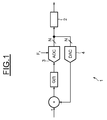
- FIG. 1 A basic diagram of a current-feedback continuous-time delta-sigma analog/digital converter, of order one, has been represented in Figure 1 . It comprises a modulator 1 of delta-sigma type followed by a decimation digital filter 2.
- the modulator 1 is here an analog/digital converter with over-sampling and shaping of the quantization noise. It comprises an analog/digital converter 3 (ADC) of low resolution, typically 1 bit, placed in a negative feedback loop which comprises a digital/analog converter 4 (DAC), and whose quantization noise is rejected towards the high frequencies by virtue of a function G(f) placed in the loop.
- ADC analog/digital converter 3
- DAC digital/analog converter 4
- G(f) digital/analog converter
- a modulator 1 of delta-sigma type comprising an analog/digital converter 3 (ADC) and a digital/analog converter 4 (DAC), and a decimation filter 2.
- ADC analog/digital converter 3
- DAC digital/analog converter 4
- decimation filter 2 a decimation filter 2.
- the modulator 1 essentially comprises an integrator 10 carrying out the function G(f) of the negative feedback loop of Figure 1 .
- This integrator 10 comprises an operational amplifier 11 and an integration capacitor C i connected between the inverting terminal and the output terminal of the amplifier 11.
- This inverting terminal is coupled to a resistor R which receives the analog input signal V in of the modulator 1.
- the non-inverting terminal of the amplifier 11 is connected to earth.
- the integrator 10 possesses, moreover, an offset voltage V 0 across the terminals of the operational amplifier 11.
- the output of the operational amplifier 11 of the integrator 10 is coupled to the converter ADC 3 which samples the output of the integrator 10 at a sampling frequency F s .
- the converter ADC 3 is coupled at output to a converter DAC 4 which is also coupled to the inverting terminal of the operational amplifier 11.
- the converter DAC 4 comprises, in this embodiment, a switched capacitive device 5, consisting of a capacitor C of which a first terminal is coupled to a discharge make/break switch 15 and a second terminal is coupled to a charge make/break switch 16, the discharge make/break switch 15 and the charge make/break switch 16 both being coupled to earth.
- the switched capacitive device 5 consists also of a positive power supply make/break switch 17 making it possible to deliver a positive reference voltage of the converter DAC 4 to the capacitor C, of a negative power supply make/break switch 18 making it possible to deliver the opposite of the reference voltage of the converter DAC 4 to the capacitor C, and of a connection make/break switch 19.
- the capacitor C charges when the charge make/break switch 16 and the positive power supply make/break switch 17 or the negative power supply make/break switch 18 are closed, whilst the other make/break switches 15 and 19 are open.
- the capacitor C discharges thereafter when the discharge make/break switch 15, and the connection make/break switch 19 are closed whilst the other make/break switches 16, 17 and 18 are open.
- the converter ADC 3 controls the converter DAC 4 on the basis of the measurement of the output signal of the integrator 10, and more particularly the power supply of the capacitor C by controlling the positive power supply make/break switch 17, and the negative power supply make/break switch 18.
- the decimation filter 2 of the current-feedback continuous-time delta-sigma analog/digital converter comprises a first counter 20 (CPT1) able to count a number of bits of a first value, and a second counter 21 (CPT2) able to count the total number of bits output by the modulator 1.
- CPT1 first counter 20
- CPT2 second counter 21
- Figure 3 illustrates a method for measuring the time constant RC of an integrated electronic circuit made up of a resistive element R and of a capacitive element C.
- a coupling is effected between the resistor R and the switched capacitive device 5, constructed on the basis of the capacitor C, at the input of the operational amplifier 11 of the integrator 10 of the modulator 1.
- a known analog input signal V in whose voltage is constant is applied at the input of the modulator 1.
- a reference voltage +V dac or -V dac of the converter DAC 4 is applied across the terminals of the switched capacitive device 5 which is switched at the sampling frequency of the converter ADC 3.
- the voltage of the output signal Q s of the modulator 1 is measured with the aid of two counters 20 and 21 of the measurement means 2.
- the value of the time constant RC is determined on the basis of at least one measurement of the level of the DC component of the signal of Q s of the modulator 1.
- an offset voltage V 0 exists across the terminals of the operational amplifier 11 of the integrator 10. This shift voltage modifies the value of the analog input voltage V in and engenders an error in the measured value of the voltage Q s .
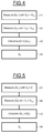
- a first mode of implementation of a method for measuring the output signal Q s making it possible to circumvent the offset voltage V 0 of the operational amplifier 11 is presented in Figure 4 .
- a step 43 the value of the second measurement Q 1 - is then subtracted from the value of the second measurement Q 1 +, and in a step 44, an output voltage value and thus a ratio of the input and reference voltages of the converter DAC 4, V in /V dac , is determined independently of the value of the offset voltage V 0 .
- a second mode of implementation of a method making it possible to circumvent the offset voltage V 0 of the operational amplifier 11 is presented in Figure 5 .
- a step 53 the measured error Q 10 due to the offset voltage V 0 is then subtracted from the voltage at the value of the second measurement Q 1 performed.
- a step 54 an output voltage value Q s is then determined independently of the value of the offset voltage V 0 .
- the output voltage is directly equal to the ratio of the impedances of the first and of the second hardware components.
- the level of the component of the output signal Q s thus measured is thus equal to the time constant RC or else to the inverse of the time constant 1/RC depending on whether the first hardware component is the resistive element or the capacitive element.
- the result of the measurement of the time constant RC can be used subsequently to calibrate a filter or any other element using the value of such a time constant RC.
Landscapes
- Compression, Expansion, Code Conversion, And Decoders (AREA)
- Analogue/Digital Conversion (AREA)
- Measurement Of Unknown Time Intervals (AREA)
Claims (11)
- System, umfassend eine integrierte elektronische Schaltung, zum Messen einer Zeitkonstante (RC) der integrierten elektronischen Schaltung (1), wobei die integrierte elektronische Schaltung (1) so konfiguriert ist, dass sie ein kontinuierliches analoges Eingangssignal (Vin) empfängt, die integrierte elektronische Schaltung (1) ferner einen Analog-Digital-Wandler (3) umfasst, der bei einer Abtastfrequenz (Fs) betrieben wird, und der Analog-Digital-Wandler so konfiguriert ist, dass er ein Ausgangssignal (Qs) der integrierten elektronischen Schaltung bereitstellt,
wobei das System eine erste Hardwarekomponente, eine zweite Hardwarekomponente und einen Digital-Analog-Wandler (4) umfasst,
das System ferner einen Operationsverstärker (11) mit einem invertierenden Anschluss umfasst, der mit einem ersten Anschluss der ersten Hardwarekomponente und mit einem ersten Anschluss der zweiten Hardwarekomponente gekoppelt ist, ein zweiter Anschluss der ersten Hardwarekomponente so konfiguriert ist, dass er das kontinuierliche analoge Eingangssignal (Vin) empfängt, und das System ferner Mittel zum Messen des Ausgangssignals der integrierten elektronischen Schaltung (1) umfasst,
das System ferner Mittel (2) umfasst, die imstande sind, den Wert der Zeitkonstante (RC) auf der Basis mindestens einer Messung der GS-Komponente des Ausgangssignals (Qs) der integrierten elektronischen Schaltung (1) zu bestimmen,
die erste Hardwarekomponente ein ohmsches Element (R) umfasst, und die zweite Hardwarekomponente ein kapazitives Element (C) umfasst,
das System ferner ein geschaltetes kapazitives Bauelement (5) umfasst, welches das kapazitive Element (C) umfasst,
das geschaltete kapazitive Bauelement im Digital-Analog-Wandler (4) enthalten ist, und jeder der zwei Anschlüsse des geschalteten kapazitiven Bauelements mit einem jeweiligen an Erde gelegten Ein-/Ausschalter (15, 16) gekoppelt ist, das Schalten des geschalteten kapazitiven Bauelements (5) bei der Abtastfrequenz (Fs) des Analog-Digital-Wandlers (3) durchgeführt wird, die Zeitkonstante entweder das Produkt oder das inverse Produkt des Widerstands des ohmschen Elements und der Kapazität des kapazitiven Elements ist. - System nach Anspruch 1,
dadurch gekennzeichnet, dass das kontinuierliche analoge Eingangssignal (Vin), das der Schaltung (1) zugeführt wird, eine Spannung ist, deren absoluter Wert der Referenzspannung (+Vdac) des Digital-Analog-Wandlers (4) der integrierten elektronischen Schaltung (1) entspricht. - System nach einem der Ansprüche 1 oder 2, dadurch gekennzeichnet, dass die Mittel (2), die zum Bestimmen des Wertes der Zeitkonstante (RC) imstande sind, ein digitales Dezimationsfilter umfassen, das an den Ausgang der integrierten elektronischen Schaltung (1) gekoppelt ist.
- System nach einem der Ansprüche 1 bis 3, dadurch gekennzeichnet, dass die Mittel (2), die zum Bestimmen des Wertes der Zeitkonstante (RC) imstande sind, einen ersten Zähler (20), der zum Zählen einer Anzahl von Bits eines ersten Wertes imstande ist, und einen zweiten Zähler (21) umfassen, der zum Zählen der Gesamtanzahl von Bits imstande ist, die durch die integrierte elektronische Schaltung (1) ausgegeben werden.
- System nach einem der Ansprüche 1 bis 4, dadurch gekennzeichnet, dass die integrierte elektronische Schaltung (1) ein Modulator vom Delta-Sigma-Typ ist.
- Verfahren zur Verwendung eines Systems nach einem der Ansprüche 1 bis 5, wobei die Zeitkonstante einer integrierten elektronischen Schaltung (1) nach einem der Ansprüche 1 bis 5, gemessen wird, wobei das Verfahren umfasst:- Koppeln eines ersten Anschlusses der ersten und der zweiten Hardwarekomponenten mit einem invertierenden Eingang des Operationsverstärkers (11),- Anlegen eines kontinuierlichen analogen Eingangssignals (Vin) an einen zweiten Anschluss der ersten Hardwarekomponente,- Messen des Ausgangssignals (Qs) der integrierten elektronischen Schaltung (1),- Bestimmen des Wertes der Zeitkonstante (RC) auf der Basis mindestens einer Messung des Pegels der GS-Komponente des Ausgangssignals (Qs) der integrierten elektronischen Schaltung (1).
- Verfahren nach Anspruch 6, wobei das kontinuierliche analoge Eingangssignal (Vin) der integrierten elektronischen Schaltung (1) eine GS-Spannung ist, deren absoluter Wert der Referenzspannung eines Digital-Analog-Wandlers (4) entspricht.
- Verfahren nach Anspruch 6 oder 7, wobei die Messung der Zeitkonstante (RC) eine erste Messung (Q1+) des Ausgangssignals (Qs) der integrierten elektronischen Schaltung (1), für welche das kontinuierliche analoge Eingangssignal (Vin) eine GS-Spannung ist, die der Referenzspannung (+Vdac) des Digital-Analog-Wandlers (4) entspricht, eine zweite Messung (Q1-) des Ausgangssignals (Qs) der integrierten elektronischen Schaltung (1), für welche das kontinuierliche analoge Eingangssignal (Vin) eine GS-Spannung ist, die der Negativen der Referenzspannung (-Vdac) des Digital-Analog-Wandlers (4) entspricht, und eine Subtraktion zwischen der ersten Messung (Q1+) und der zweiten Messung (Q1-) umfasst.
- Verfahren nach Anspruch 6, wobei die Messung der Zeitkonstante (RC) eine Nicht-Last-Messung (Q10) des Ausgangssignals (Qs) der integrierten elektronischen Schaltung (1), für welche das kontinuierliche analoge Eingangssignal (Vin) eine GS-Nullspannung ist, eine Anfangsmessung (Q1) des Ausgangssignals (Qs) der Schaltung (1), für welche das kontinuierliche analoge Eingangssignal (Vin) eine GS-Spannung ist, die der Referenzspannung (+Vdac) des Digital-Analog-Wandlers (4) entspricht, und eine Subtraktion zwischen der Nicht-Last-Messung (Q10) und der Anfangsmessung (Q1) umfasst.
- Verfahren nach einem der Ansprüche 6 bis 9, dadurch gekennzeichnet, dass die integrierte Schaltung ein Modulator vom Delta-Sigma-Typ ist.
- Verfahren zur automatischen Kalibrierung einer Zeitkonstante (RC) einer integrierten elektronischen Schaltung (1), wobei die Zeitkonstante (RC) von einer ersten Hardwarekomponente und einer zweiten Hardwarekomponente gebildet wird, dadurch gekennzeichnet, dass das Verfahren zur Messung der Zeitkonstante (RC) der integrierten elektronischen Schaltung (1) nach einem der Ansprüche 6 bis 10 zum Kalibrieren der Zeitkonstante (RC) der elektronischen Schaltung (1) verwendet wird, wobei die Zeitkonstante (RC) von der ersten Hardwarekomponente und der zweiten Hardwarekomponente gebildet wird.
Applications Claiming Priority (2)
| Application Number | Priority Date | Filing Date | Title |
|---|---|---|---|
| FR0950524 | 2009-01-28 | ||
| PCT/EP2010/050966 WO2010086348A2 (en) | 2009-01-28 | 2010-01-28 | Method and system for measuring a time constant of an integrated circuit, and integrated circuit provided with such a system |
Publications (2)
| Publication Number | Publication Date |
|---|---|
| EP2382709A2 EP2382709A2 (de) | 2011-11-02 |
| EP2382709B1 true EP2382709B1 (de) | 2016-08-17 |
Family
ID=40983416
Family Applications (1)
| Application Number | Title | Priority Date | Filing Date |
|---|---|---|---|
| EP10701529.9A Not-in-force EP2382709B1 (de) | 2009-01-28 | 2010-01-28 | Verfahren und system zur messung einer zeitkonstante einer integrierten schaltung und integrierte schaltung mit derartigem system |
Country Status (3)
| Country | Link |
|---|---|
| US (1) | US9030213B2 (de) |
| EP (1) | EP2382709B1 (de) |
| WO (1) | WO2010086348A2 (de) |
Families Citing this family (5)
| Publication number | Priority date | Publication date | Assignee | Title |
|---|---|---|---|---|
| KR20120089177A (ko) * | 2011-02-01 | 2012-08-09 | 삼성전자주식회사 | 오디오 신호 출력 방법 및 그에 따른 오디오 신호 출력 장치 |
| US8884635B2 (en) * | 2012-06-01 | 2014-11-11 | Synaptics Incorporated | Transcapacitive charge measurement |
| US8890544B2 (en) * | 2012-06-01 | 2014-11-18 | Synaptics Incorporated | Transcapacitive charge measurement |
| DE102013014810B4 (de) | 2013-09-05 | 2019-03-14 | Elmos Semiconductor Aktiengesellschaft | Vorrichtung zum Betreiben passiver Infrarotsensoren |
| US12472316B2 (en) * | 2016-09-09 | 2025-11-18 | Rai Strategic Holdings, Inc. | Analog control component for an aerosol delivery device |
Citations (2)
| Publication number | Priority date | Publication date | Assignee | Title |
|---|---|---|---|---|
| US5245646A (en) * | 1992-06-01 | 1993-09-14 | Motorola, Inc. | Tuning circuit for use with an integrated continuous time analog filter |
| US20040124911A1 (en) * | 2001-05-03 | 2004-07-01 | Christian Fleischhacker | Method and apparatus for adjusting an active filter |
Family Cites Families (19)
| Publication number | Priority date | Publication date | Assignee | Title |
|---|---|---|---|---|
| US5150324A (en) * | 1988-06-09 | 1992-09-22 | Asahi Kasei Microsystems Co. Ltd. | Analog arithmetic circuit that can perform multiplication division expansion and compression by using delta sigma modulator |
| EP0523306B1 (de) * | 1991-07-17 | 1995-10-25 | International Business Machines Corporation | Dezimationsfilter für Sigma-Delta Konverter und Datenendeinrichtung mit einem solchen Filter |
| US5621329A (en) * | 1995-04-13 | 1997-04-15 | Industrial Technology Research Institute | Automatic self-calibration system for digital teraohmmeter |
| JPH10322214A (ja) * | 1997-05-15 | 1998-12-04 | Nippon Baa Braun Kk | オフセット除去機能付のアナログ−デジタル変換器 |
| US5914633A (en) | 1997-08-08 | 1999-06-22 | Lucent Technologies Inc. | Method and apparatus for tuning a continuous time filter |
| FR2775141B1 (fr) | 1998-02-19 | 2002-10-11 | Sgs Thomson Microelectronics | Dispositif d'etalonnage de constantes de temps |
| US6262603B1 (en) | 2000-02-29 | 2001-07-17 | National Semiconductor Corporation | RC calibration circuit with reduced power consumption and increased accuracy |
| FR2805940B1 (fr) * | 2000-03-01 | 2002-05-31 | France Telecom | Systeme de correction du cna pour modulateur delta sigma |
| US6433713B1 (en) | 2001-05-31 | 2002-08-13 | Agilent Technologies, Inc. | Calibration of analog-to-digital converters |
| CN100581050C (zh) * | 2003-02-11 | 2010-01-13 | Nxp股份有限公司 | 用于临界连续时间应用的自调零方法和设备 |
| US6803813B1 (en) | 2003-04-22 | 2004-10-12 | National Semiconductor Corporation | Time constant-based calibration circuit for active filters |
| DE10321200B3 (de) | 2003-05-12 | 2005-02-03 | Infineon Technologies Ag | Einrichtung und Verfahren zur Kalibrierung von R/C-Filterschaltungen |
| US7230555B2 (en) * | 2005-02-23 | 2007-06-12 | Analogic Corporation | Sigma delta converter with flying capacitor input |
| US7142144B1 (en) * | 2005-05-19 | 2006-11-28 | Ami Semiconductor, Inc. | Low power sigma delta modulator |
| US7301350B2 (en) * | 2005-06-03 | 2007-11-27 | Synaptics Incorporated | Methods and systems for detecting a capacitance using sigma-delta measurement techniques |
| US7324028B2 (en) * | 2005-09-23 | 2008-01-29 | Realtek Semiconductor Corp. | Self-calibrating continuous-time delta-sigma modulator |
| CN101305520B (zh) * | 2005-11-11 | 2010-05-19 | Nxp股份有限公司 | 包括西格马德尔塔模-数转换器的信号处理电路 |
| US7969339B2 (en) * | 2006-03-23 | 2011-06-28 | Freescale Semiconductor, Inc. | Electronic device and integrated circuit comprising a delta-sigma converter and method therefor |
| US7982526B2 (en) * | 2008-09-17 | 2011-07-19 | Qualcomm, Incorporated | Active-time dependent bias current generation for switched-capacitor circuits |
-
2010
- 2010-01-28 EP EP10701529.9A patent/EP2382709B1/de not_active Not-in-force
- 2010-01-28 WO PCT/EP2010/050966 patent/WO2010086348A2/en not_active Ceased
- 2010-01-28 US US13/148,274 patent/US9030213B2/en active Active
Patent Citations (2)
| Publication number | Priority date | Publication date | Assignee | Title |
|---|---|---|---|---|
| US5245646A (en) * | 1992-06-01 | 1993-09-14 | Motorola, Inc. | Tuning circuit for use with an integrated continuous time analog filter |
| US20040124911A1 (en) * | 2001-05-03 | 2004-07-01 | Christian Fleischhacker | Method and apparatus for adjusting an active filter |
Also Published As
| Publication number | Publication date |
|---|---|
| EP2382709A2 (de) | 2011-11-02 |
| US20120025847A1 (en) | 2012-02-02 |
| US9030213B2 (en) | 2015-05-12 |
| WO2010086348A3 (en) | 2010-12-23 |
| WO2010086348A2 (en) | 2010-08-05 |
Similar Documents
| Publication | Publication Date | Title |
|---|---|---|
| CN1977458B (zh) | 用于连续时间的增量累加模数转换器的混合调谐电路 | |
| US10177781B2 (en) | Circuit including a switched capacitor bridge and method | |
| TWI332323B (en) | A/d converter and a/d converting method | |
| JP2994497B2 (ja) | D/aコンバータのdcオフセットキャリブレーション方法とd/aコンバータのdcオフセットキャリブレーションシステム | |
| JP6038814B2 (ja) | アナログデジタル変換器 | |
| AU758094B2 (en) | Method and apparatus for eliminating clock jitter in continuous-time delta-sigma analog-to-digital converters | |
| WO2010147713A1 (en) | Switched capacitor notch filter | |
| US11031949B2 (en) | Analog-to-digital converter, sensor arrangement and method for analog-to-digital conversion | |
| JP7530549B2 (ja) | センサでの寄生容量不感サンプリング | |
| US9030213B2 (en) | Method and system for measuring a time constant of an integrated circuit, and integrated circuit provided with such a system | |
| CN112448722A (zh) | 基准电压噪声的滤波方法 | |
| US11962331B2 (en) | Sigma-delta analog-to-digital converter | |
| US20130093467A1 (en) | Foreground techniques for comparator calibration | |
| WO2012091788A1 (en) | Calibration of time constants in a continuous-time delta-sigma converter | |
| CN117318725A (zh) | 连续时间∑-δ模数转换器 | |
| CN111865309A (zh) | 增量式模拟数字转换器 | |
| US20070024485A1 (en) | Reducing Variation in Reference Voltage When the Load Varies Dynamically | |
| US20140240022A1 (en) | Charge measurement | |
| US12438552B2 (en) | ΔΣmodulation utilizing continuous-time input and discrete-time loop filter | |
| US20120026024A1 (en) | System for calibrating a time constant of an integrated circuit, and integrated circuit provided with such a system | |
| EP4518160A1 (de) | Analog-digital-wandler mit register mit schrittweiser annäherung und programmierbarer abtastrauschunterdrückung | |
| US10305507B1 (en) | First-order sigma-delta analog-to-digital converter | |
| EP1324498B1 (de) | Verfahren zur Selbstkalibrierung eines Phasen-Integrationsfehlers in einem Modulator | |
| Schlarmann et al. | Technique to eliminate slow-settling components that appear due to dipoles [multipath compensated amplifiers] | |
| JP2026005249A (ja) | コモン電圧生成回路、及びこれを用いたスイッチトキャパシタ回路 |
Legal Events
| Date | Code | Title | Description |
|---|---|---|---|
| PUAI | Public reference made under article 153(3) epc to a published international application that has entered the european phase |
Free format text: ORIGINAL CODE: 0009012 |
|
| 17P | Request for examination filed |
Effective date: 20110729 |
|
| AK | Designated contracting states |
Kind code of ref document: A2 Designated state(s): AT BE BG CH CY CZ DE DK EE ES FI FR GB GR HR HU IE IS IT LI LT LU LV MC MK MT NL NO PL PT RO SE SI SK SM TR |
|
| DAX | Request for extension of the european patent (deleted) | ||
| 17Q | First examination report despatched |
Effective date: 20140401 |
|
| GRAP | Despatch of communication of intention to grant a patent |
Free format text: ORIGINAL CODE: EPIDOSNIGR1 |
|
| INTG | Intention to grant announced |
Effective date: 20160324 |
|
| GRAS | Grant fee paid |
Free format text: ORIGINAL CODE: EPIDOSNIGR3 |
|
| GRAA | (expected) grant |
Free format text: ORIGINAL CODE: 0009210 |
|
| AK | Designated contracting states |
Kind code of ref document: B1 Designated state(s): AT BE BG CH CY CZ DE DK EE ES FI FR GB GR HR HU IE IS IT LI LT LU LV MC MK MT NL NO PL PT RO SE SI SK SM TR |
|
| REG | Reference to a national code |
Ref country code: GB Ref legal event code: FG4D |
|
| REG | Reference to a national code |
Ref country code: CH Ref legal event code: EP |
|
| REG | Reference to a national code |
Ref country code: IE Ref legal event code: FG4D |
|
| REG | Reference to a national code |
Ref country code: AT Ref legal event code: REF Ref document number: 821914 Country of ref document: AT Kind code of ref document: T Effective date: 20160915 |
|
| REG | Reference to a national code |
Ref country code: DE Ref legal event code: R096 Ref document number: 602010035569 Country of ref document: DE |
|
| REG | Reference to a national code |
Ref country code: FR Ref legal event code: PLFP Year of fee payment: 8 Ref country code: NL Ref legal event code: MP Effective date: 20160817 |
|
| REG | Reference to a national code |
Ref country code: LT Ref legal event code: MG4D |
|
| REG | Reference to a national code |
Ref country code: DE Ref legal event code: R082 Ref document number: 602010035569 Country of ref document: DE Representative=s name: GRUENECKER PATENT- UND RECHTSANWAELTE PARTG MB, DE Ref country code: DE Ref legal event code: R081 Ref document number: 602010035569 Country of ref document: DE Owner name: OCT CIRCUIT TECHNOLOGIES INTERNATIONAL LTD., IE Free format text: FORMER OWNER: ST-ERICSSON SA, PLAN-LES-OUATES, CH |
|
| REG | Reference to a national code |
Ref country code: AT Ref legal event code: MK05 Ref document number: 821914 Country of ref document: AT Kind code of ref document: T Effective date: 20160817 |
|
| RAP2 | Party data changed (patent owner data changed or rights of a patent transferred) |
Owner name: OCT CIRCUIT TECHNOLOGIES INTERNATIONAL LIMITED |
|
| PG25 | Lapsed in a contracting state [announced via postgrant information from national office to epo] |
Ref country code: FI Free format text: LAPSE BECAUSE OF FAILURE TO SUBMIT A TRANSLATION OF THE DESCRIPTION OR TO PAY THE FEE WITHIN THE PRESCRIBED TIME-LIMIT Effective date: 20160817 Ref country code: NO Free format text: LAPSE BECAUSE OF FAILURE TO SUBMIT A TRANSLATION OF THE DESCRIPTION OR TO PAY THE FEE WITHIN THE PRESCRIBED TIME-LIMIT Effective date: 20161117 Ref country code: LT Free format text: LAPSE BECAUSE OF FAILURE TO SUBMIT A TRANSLATION OF THE DESCRIPTION OR TO PAY THE FEE WITHIN THE PRESCRIBED TIME-LIMIT Effective date: 20160817 Ref country code: HR Free format text: LAPSE BECAUSE OF FAILURE TO SUBMIT A TRANSLATION OF THE DESCRIPTION OR TO PAY THE FEE WITHIN THE PRESCRIBED TIME-LIMIT Effective date: 20160817 Ref country code: IT Free format text: LAPSE BECAUSE OF FAILURE TO SUBMIT A TRANSLATION OF THE DESCRIPTION OR TO PAY THE FEE WITHIN THE PRESCRIBED TIME-LIMIT Effective date: 20160817 Ref country code: NL Free format text: LAPSE BECAUSE OF FAILURE TO SUBMIT A TRANSLATION OF THE DESCRIPTION OR TO PAY THE FEE WITHIN THE PRESCRIBED TIME-LIMIT Effective date: 20160817 |
|
| PG25 | Lapsed in a contracting state [announced via postgrant information from national office to epo] |
Ref country code: ES Free format text: LAPSE BECAUSE OF FAILURE TO SUBMIT A TRANSLATION OF THE DESCRIPTION OR TO PAY THE FEE WITHIN THE PRESCRIBED TIME-LIMIT Effective date: 20160817 Ref country code: PT Free format text: LAPSE BECAUSE OF FAILURE TO SUBMIT A TRANSLATION OF THE DESCRIPTION OR TO PAY THE FEE WITHIN THE PRESCRIBED TIME-LIMIT Effective date: 20161219 Ref country code: LV Free format text: LAPSE BECAUSE OF FAILURE TO SUBMIT A TRANSLATION OF THE DESCRIPTION OR TO PAY THE FEE WITHIN THE PRESCRIBED TIME-LIMIT Effective date: 20160817 Ref country code: GR Free format text: LAPSE BECAUSE OF FAILURE TO SUBMIT A TRANSLATION OF THE DESCRIPTION OR TO PAY THE FEE WITHIN THE PRESCRIBED TIME-LIMIT Effective date: 20161118 Ref country code: SE Free format text: LAPSE BECAUSE OF FAILURE TO SUBMIT A TRANSLATION OF THE DESCRIPTION OR TO PAY THE FEE WITHIN THE PRESCRIBED TIME-LIMIT Effective date: 20160817 Ref country code: AT Free format text: LAPSE BECAUSE OF FAILURE TO SUBMIT A TRANSLATION OF THE DESCRIPTION OR TO PAY THE FEE WITHIN THE PRESCRIBED TIME-LIMIT Effective date: 20160817 Ref country code: PL Free format text: LAPSE BECAUSE OF FAILURE TO SUBMIT A TRANSLATION OF THE DESCRIPTION OR TO PAY THE FEE WITHIN THE PRESCRIBED TIME-LIMIT Effective date: 20160817 |
|
| PG25 | Lapsed in a contracting state [announced via postgrant information from national office to epo] |
Ref country code: EE Free format text: LAPSE BECAUSE OF FAILURE TO SUBMIT A TRANSLATION OF THE DESCRIPTION OR TO PAY THE FEE WITHIN THE PRESCRIBED TIME-LIMIT Effective date: 20160817 Ref country code: RO Free format text: LAPSE BECAUSE OF FAILURE TO SUBMIT A TRANSLATION OF THE DESCRIPTION OR TO PAY THE FEE WITHIN THE PRESCRIBED TIME-LIMIT Effective date: 20160817 |
|
| REG | Reference to a national code |
Ref country code: DE Ref legal event code: R097 Ref document number: 602010035569 Country of ref document: DE |
|
| PG25 | Lapsed in a contracting state [announced via postgrant information from national office to epo] |
Ref country code: DK Free format text: LAPSE BECAUSE OF FAILURE TO SUBMIT A TRANSLATION OF THE DESCRIPTION OR TO PAY THE FEE WITHIN THE PRESCRIBED TIME-LIMIT Effective date: 20160817 Ref country code: SM Free format text: LAPSE BECAUSE OF FAILURE TO SUBMIT A TRANSLATION OF THE DESCRIPTION OR TO PAY THE FEE WITHIN THE PRESCRIBED TIME-LIMIT Effective date: 20160817 Ref country code: CZ Free format text: LAPSE BECAUSE OF FAILURE TO SUBMIT A TRANSLATION OF THE DESCRIPTION OR TO PAY THE FEE WITHIN THE PRESCRIBED TIME-LIMIT Effective date: 20160817 Ref country code: BG Free format text: LAPSE BECAUSE OF FAILURE TO SUBMIT A TRANSLATION OF THE DESCRIPTION OR TO PAY THE FEE WITHIN THE PRESCRIBED TIME-LIMIT Effective date: 20161117 Ref country code: SK Free format text: LAPSE BECAUSE OF FAILURE TO SUBMIT A TRANSLATION OF THE DESCRIPTION OR TO PAY THE FEE WITHIN THE PRESCRIBED TIME-LIMIT Effective date: 20160817 Ref country code: BE Free format text: LAPSE BECAUSE OF FAILURE TO SUBMIT A TRANSLATION OF THE DESCRIPTION OR TO PAY THE FEE WITHIN THE PRESCRIBED TIME-LIMIT Effective date: 20160817 |
|
| PLBE | No opposition filed within time limit |
Free format text: ORIGINAL CODE: 0009261 |
|
| STAA | Information on the status of an ep patent application or granted ep patent |
Free format text: STATUS: NO OPPOSITION FILED WITHIN TIME LIMIT |
|
| 26N | No opposition filed |
Effective date: 20170518 |
|
| PG25 | Lapsed in a contracting state [announced via postgrant information from national office to epo] |
Ref country code: SI Free format text: LAPSE BECAUSE OF FAILURE TO SUBMIT A TRANSLATION OF THE DESCRIPTION OR TO PAY THE FEE WITHIN THE PRESCRIBED TIME-LIMIT Effective date: 20160817 |
|
| REG | Reference to a national code |
Ref country code: CH Ref legal event code: PL |
|
| PG25 | Lapsed in a contracting state [announced via postgrant information from national office to epo] |
Ref country code: MC Free format text: LAPSE BECAUSE OF FAILURE TO SUBMIT A TRANSLATION OF THE DESCRIPTION OR TO PAY THE FEE WITHIN THE PRESCRIBED TIME-LIMIT Effective date: 20160817 |
|
| PG25 | Lapsed in a contracting state [announced via postgrant information from national office to epo] |
Ref country code: CH Free format text: LAPSE BECAUSE OF NON-PAYMENT OF DUE FEES Effective date: 20170131 Ref country code: LI Free format text: LAPSE BECAUSE OF NON-PAYMENT OF DUE FEES Effective date: 20170131 |
|
| REG | Reference to a national code |
Ref country code: IE Ref legal event code: MM4A |
|
| PG25 | Lapsed in a contracting state [announced via postgrant information from national office to epo] |
Ref country code: LU Free format text: LAPSE BECAUSE OF NON-PAYMENT OF DUE FEES Effective date: 20170128 |
|
| REG | Reference to a national code |
Ref country code: FR Ref legal event code: PLFP Year of fee payment: 9 |
|
| PG25 | Lapsed in a contracting state [announced via postgrant information from national office to epo] |
Ref country code: IE Free format text: LAPSE BECAUSE OF NON-PAYMENT OF DUE FEES Effective date: 20170128 |
|
| PG25 | Lapsed in a contracting state [announced via postgrant information from national office to epo] |
Ref country code: MT Free format text: LAPSE BECAUSE OF NON-PAYMENT OF DUE FEES Effective date: 20170128 |
|
| PG25 | Lapsed in a contracting state [announced via postgrant information from national office to epo] |
Ref country code: HU Free format text: LAPSE BECAUSE OF FAILURE TO SUBMIT A TRANSLATION OF THE DESCRIPTION OR TO PAY THE FEE WITHIN THE PRESCRIBED TIME-LIMIT; INVALID AB INITIO Effective date: 20100128 |
|
| PG25 | Lapsed in a contracting state [announced via postgrant information from national office to epo] |
Ref country code: CY Free format text: LAPSE BECAUSE OF NON-PAYMENT OF DUE FEES Effective date: 20160817 |
|
| PG25 | Lapsed in a contracting state [announced via postgrant information from national office to epo] |
Ref country code: MK Free format text: LAPSE BECAUSE OF FAILURE TO SUBMIT A TRANSLATION OF THE DESCRIPTION OR TO PAY THE FEE WITHIN THE PRESCRIBED TIME-LIMIT Effective date: 20160817 |
|
| PG25 | Lapsed in a contracting state [announced via postgrant information from national office to epo] |
Ref country code: TR Free format text: LAPSE BECAUSE OF FAILURE TO SUBMIT A TRANSLATION OF THE DESCRIPTION OR TO PAY THE FEE WITHIN THE PRESCRIBED TIME-LIMIT Effective date: 20160817 |
|
| PG25 | Lapsed in a contracting state [announced via postgrant information from national office to epo] |
Ref country code: IS Free format text: LAPSE BECAUSE OF FAILURE TO SUBMIT A TRANSLATION OF THE DESCRIPTION OR TO PAY THE FEE WITHIN THE PRESCRIBED TIME-LIMIT Effective date: 20161217 |
|
| REG | Reference to a national code |
Ref country code: GB Ref legal event code: 732E Free format text: REGISTERED BETWEEN 20210722 AND 20210728 |
|
| REG | Reference to a national code |
Ref country code: GB Ref legal event code: 732E Free format text: REGISTERED BETWEEN 20210805 AND 20210811 |
|
| PGFP | Annual fee paid to national office [announced via postgrant information from national office to epo] |
Ref country code: FR Payment date: 20230125 Year of fee payment: 14 |
|
| PGFP | Annual fee paid to national office [announced via postgrant information from national office to epo] |
Ref country code: GB Payment date: 20230127 Year of fee payment: 14 Ref country code: DE Payment date: 20230127 Year of fee payment: 14 |
|
| REG | Reference to a national code |
Ref country code: DE Ref legal event code: R119 Ref document number: 602010035569 Country of ref document: DE |
|
| GBPC | Gb: european patent ceased through non-payment of renewal fee |
Effective date: 20240128 |
|
| PG25 | Lapsed in a contracting state [announced via postgrant information from national office to epo] |
Ref country code: DE Free format text: LAPSE BECAUSE OF NON-PAYMENT OF DUE FEES Effective date: 20240801 |
|
| PG25 | Lapsed in a contracting state [announced via postgrant information from national office to epo] |
Ref country code: GB Free format text: LAPSE BECAUSE OF NON-PAYMENT OF DUE FEES Effective date: 20240128 |
|
| PG25 | Lapsed in a contracting state [announced via postgrant information from national office to epo] |
Ref country code: FR Free format text: LAPSE BECAUSE OF NON-PAYMENT OF DUE FEES Effective date: 20240131 |
|
| PG25 | Lapsed in a contracting state [announced via postgrant information from national office to epo] |
Ref country code: GB Free format text: LAPSE BECAUSE OF NON-PAYMENT OF DUE FEES Effective date: 20240128 Ref country code: FR Free format text: LAPSE BECAUSE OF NON-PAYMENT OF DUE FEES Effective date: 20240131 Ref country code: DE Free format text: LAPSE BECAUSE OF NON-PAYMENT OF DUE FEES Effective date: 20240801 |