EP2383780A1 - Lichtemittierende Vorrichtungen - Google Patents
Lichtemittierende Vorrichtungen Download PDFInfo
- Publication number
- EP2383780A1 EP2383780A1 EP20100172281 EP10172281A EP2383780A1 EP 2383780 A1 EP2383780 A1 EP 2383780A1 EP 20100172281 EP20100172281 EP 20100172281 EP 10172281 A EP10172281 A EP 10172281A EP 2383780 A1 EP2383780 A1 EP 2383780A1
- Authority
- EP
- European Patent Office
- Prior art keywords
- light emitting
- patterned
- conductive layer
- emitting device
- layer
- Prior art date
- Legal status (The legal status is an assumption and is not a legal conclusion. Google has not performed a legal analysis and makes no representation as to the accuracy of the status listed.)
- Withdrawn
Links
Images


Classifications
-
- H—ELECTRICITY
- H10—SEMICONDUCTOR DEVICES; ELECTRIC SOLID-STATE DEVICES NOT OTHERWISE PROVIDED FOR
- H10W—GENERIC PACKAGES, INTERCONNECTIONS, CONNECTORS OR OTHER CONSTRUCTIONAL DETAILS OF DEVICES COVERED BY CLASS H10
- H10W90/00—Package configurations
-
- H—ELECTRICITY
- H05—ELECTRIC TECHNIQUES NOT OTHERWISE PROVIDED FOR
- H05K—PRINTED CIRCUITS; CASINGS OR CONSTRUCTIONAL DETAILS OF ELECTRIC APPARATUS; MANUFACTURE OF ASSEMBLAGES OF ELECTRICAL COMPONENTS
- H05K1/00—Printed circuits
- H05K1/02—Details
- H05K1/11—Printed elements for providing electric connections to or between printed circuits
- H05K1/111—Pads for surface mounting, e.g. lay-out
-
- H—ELECTRICITY
- H05—ELECTRIC TECHNIQUES NOT OTHERWISE PROVIDED FOR
- H05K—PRINTED CIRCUITS; CASINGS OR CONSTRUCTIONAL DETAILS OF ELECTRIC APPARATUS; MANUFACTURE OF ASSEMBLAGES OF ELECTRICAL COMPONENTS
- H05K2201/00—Indexing scheme relating to printed circuits covered by H05K1/00
- H05K2201/03—Conductive materials
- H05K2201/0332—Structure of the conductor
- H05K2201/0388—Other aspects of conductors
- H05K2201/0391—Using different types of conductors
-
- H—ELECTRICITY
- H05—ELECTRIC TECHNIQUES NOT OTHERWISE PROVIDED FOR
- H05K—PRINTED CIRCUITS; CASINGS OR CONSTRUCTIONAL DETAILS OF ELECTRIC APPARATUS; MANUFACTURE OF ASSEMBLAGES OF ELECTRICAL COMPONENTS
- H05K2201/00—Indexing scheme relating to printed circuits covered by H05K1/00
- H05K2201/10—Details of components or other objects attached to or integrated in a printed circuit board
- H05K2201/10007—Types of components
- H05K2201/10106—Light emitting diode [LED]
-
- H—ELECTRICITY
- H05—ELECTRIC TECHNIQUES NOT OTHERWISE PROVIDED FOR
- H05K—PRINTED CIRCUITS; CASINGS OR CONSTRUCTIONAL DETAILS OF ELECTRIC APPARATUS; MANUFACTURE OF ASSEMBLAGES OF ELECTRICAL COMPONENTS
- H05K2201/00—Indexing scheme relating to printed circuits covered by H05K1/00
- H05K2201/20—Details of printed circuits not provided for in H05K2201/01 - H05K2201/10
- H05K2201/2054—Light-reflecting surface, e.g. conductors, substrates, coatings, dielectrics
-
- H—ELECTRICITY
- H10—SEMICONDUCTOR DEVICES; ELECTRIC SOLID-STATE DEVICES NOT OTHERWISE PROVIDED FOR
- H10H—INORGANIC LIGHT-EMITTING SEMICONDUCTOR DEVICES HAVING POTENTIAL BARRIERS
- H10H20/00—Individual inorganic light-emitting semiconductor devices having potential barriers, e.g. light-emitting diodes [LED]
- H10H20/80—Constructional details
- H10H20/83—Electrodes
- H10H20/832—Electrodes characterised by their material
- H10H20/835—Reflective materials
-
- H—ELECTRICITY
- H10—SEMICONDUCTOR DEVICES; ELECTRIC SOLID-STATE DEVICES NOT OTHERWISE PROVIDED FOR
- H10H—INORGANIC LIGHT-EMITTING SEMICONDUCTOR DEVICES HAVING POTENTIAL BARRIERS
- H10H20/00—Individual inorganic light-emitting semiconductor devices having potential barriers, e.g. light-emitting diodes [LED]
- H10H20/80—Constructional details
- H10H20/84—Coatings, e.g. passivation layers or antireflective coatings
- H10H20/841—Reflective coatings, e.g. dielectric Bragg reflectors
-
- H—ELECTRICITY
- H10—SEMICONDUCTOR DEVICES; ELECTRIC SOLID-STATE DEVICES NOT OTHERWISE PROVIDED FOR
- H10H—INORGANIC LIGHT-EMITTING SEMICONDUCTOR DEVICES HAVING POTENTIAL BARRIERS
- H10H20/00—Individual inorganic light-emitting semiconductor devices having potential barriers, e.g. light-emitting diodes [LED]
- H10H20/80—Constructional details
- H10H20/85—Packages
- H10H20/855—Optical field-shaping means, e.g. lenses
- H10H20/856—Reflecting means
-
- H—ELECTRICITY
- H10—SEMICONDUCTOR DEVICES; ELECTRIC SOLID-STATE DEVICES NOT OTHERWISE PROVIDED FOR
- H10W—GENERIC PACKAGES, INTERCONNECTIONS, CONNECTORS OR OTHER CONSTRUCTIONAL DETAILS OF DEVICES COVERED BY CLASS H10
- H10W72/00—Interconnections or connectors in packages
- H10W72/50—Bond wires
- H10W72/531—Shapes of wire connectors
- H10W72/536—Shapes of wire connectors the connected ends being ball-shaped
-
- H—ELECTRICITY
- H10—SEMICONDUCTOR DEVICES; ELECTRIC SOLID-STATE DEVICES NOT OTHERWISE PROVIDED FOR
- H10W—GENERIC PACKAGES, INTERCONNECTIONS, CONNECTORS OR OTHER CONSTRUCTIONAL DETAILS OF DEVICES COVERED BY CLASS H10
- H10W72/00—Interconnections or connectors in packages
- H10W72/50—Bond wires
- H10W72/551—Materials of bond wires
- H10W72/552—Materials of bond wires comprising metals or metalloids, e.g. silver
- H10W72/5522—Materials of bond wires comprising metals or metalloids, e.g. silver comprising gold [Au]
-
- H—ELECTRICITY
- H10—SEMICONDUCTOR DEVICES; ELECTRIC SOLID-STATE DEVICES NOT OTHERWISE PROVIDED FOR
- H10W—GENERIC PACKAGES, INTERCONNECTIONS, CONNECTORS OR OTHER CONSTRUCTIONAL DETAILS OF DEVICES COVERED BY CLASS H10
- H10W90/00—Package configurations
- H10W90/701—Package configurations characterised by the relative positions of pads or connectors relative to package parts
- H10W90/751—Package configurations characterised by the relative positions of pads or connectors relative to package parts of bond wires
- H10W90/753—Package configurations characterised by the relative positions of pads or connectors relative to package parts of bond wires between laterally-adjacent chips
-
- Y—GENERAL TAGGING OF NEW TECHNOLOGICAL DEVELOPMENTS; GENERAL TAGGING OF CROSS-SECTIONAL TECHNOLOGIES SPANNING OVER SEVERAL SECTIONS OF THE IPC; TECHNICAL SUBJECTS COVERED BY FORMER USPC CROSS-REFERENCE ART COLLECTIONS [XRACs] AND DIGESTS
- Y02—TECHNOLOGIES OR APPLICATIONS FOR MITIGATION OR ADAPTATION AGAINST CLIMATE CHANGE
- Y02P—CLIMATE CHANGE MITIGATION TECHNOLOGIES IN THE PRODUCTION OR PROCESSING OF GOODS
- Y02P70/00—Climate change mitigation technologies in the production process for final industrial or consumer products
- Y02P70/50—Manufacturing or production processes characterised by the final manufactured product
Definitions
- the present invention generally relates to an optoelectronic device and, more particularly, to a light emitting device.
- a light emitting device may include light emitting units arranged over a substrate. Between the light-emitting units and the substrate, a conductive layer may be provided for conducting power to and therefore activating the light-emitting units. Furthermore, the conductive layer may include separate regions for mounting the light-emitting units and conductive wires thereon. Moreover, the conductive layer may reflect the beams of light emitted by the light-emitting units, as will be discussed below.
- FIG. 1 is a schematic plan view of a light emitting device 100 in prior art.
- the light emitting device 100 may include a substrate 10, a die attachment region 11 and a wire bond region 12 defined over the substrate 10, and a patterned conductive layer 13.
- the patterned conductive layer 13 may include first pads 131 in the die attachment region 11 and second pads 132 in the wire bond region 12.
- At least one chip or die 18 each serving as a light emitting unit of the light emitting device 100 may be attached to the first pads 131 and electrically interconnected with each other or electrically coupled by wires 17 to the second pads 132 in order for electrical connection with external circuits.
- the first and second pads 131 and 132 of the patterned conductive layer 13 may be formed of gold (Au) or silver (Ag).
- Au may exhibit good bonding reliability for die attachment and wire bond.
- Au may not provide high reflectivity over the spectrum of visible light.
- silver (Ag) may exhibit relatively high reflectivity in the full spectrum of visible light. Nevertheless, Ag may suffer sulfurization, which may adversely affect the reflectivity.
- Ag may be subject to a migration issue, which may lead to short-circuiting in the light emitting device 100.
- Examples of the present invention may provide a light emitting device that comprises a substrate, a patterned first conductive layer over the substrate, wherein the patterned first conductive layer is formed of aluminum (Al), a pattern second conductive layer on the patterned first conductive layer, wherein the patterned second conductive layer is formed of a material selected from one of gold (Au) and silver (Ag), and a reflective layer on the patterned first conductive layer, exposing the patterned second conductive layer.
- a light emitting device that comprises a substrate, a patterned first conductive layer over the substrate, wherein the patterned first conductive layer is formed of aluminum (Al), a pattern second conductive layer on the patterned first conductive layer, wherein the patterned second conductive layer is formed of a material selected from one of gold (Au) and silver (Ag), and a reflective layer on the patterned first conductive layer, exposing the patterned second conductive layer.
- Some examples of the present invention may provide a light emitting device that comprises a number of light emitting chips, a substrate to support the light emitting chips, a patterned first conductive layer over the substrate to facilitate radiation and reflection of light from the light emitting chips, and a pattern second conductive layer on the patterned first conductive layer, wherein the light emitting chips are located on the patterned second conductive layer.
- Examples of the present invention may also provide a light emitting device that comprises a substrate including a first region and a second region, the first and second regions located immediately adjacent to each other, a number of first units in the first region to facilitate radiation and reflection of light, a number of second units in the second region to facilitate radiation and reflection of light, a number of first pads on the first units, a number of second pads on the second units, and a number of light emitting chips on the second pads.
- FIG. 1 is a schematic plan view of a light emitting device in prior art
- FIG. 2A is a schematic plan view of a light emitting device in accordance with an example of the present invention.
- FIG. 2B is a schematic perspective view of a light emitting chip illustrated in FIG. 2A ;
- FIG. 2C is a schematic cross-sectional view of the light emitting device illustrated in FIG. 2A ;
- FIG. 3A is a schematic plan view of a light emitting device in accordance with another example of the present invention.
- FIG. 3B is a schematic perspective view of a light emitting chip illustrated in FIG. 3A ;
- FIG. 3C is a schematic cross-sectional view of the light emitting device illustrated in FIG. 3A ;
- FIG. 4A is a schematic plan view of a light emitting device in accordance with still another example of the present invention.
- FIG. 4B is a schematic cross-sectional view of the light emitting device illustrated in FIG. 4A ;
- FIG. 5A is a schematic plan view of a light emitting device in accordance with yet another example of the present invention.
- FIG. 5B is a schematic cross-sectional view of the light emitting device illustrated in FIG. 5A .
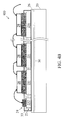
- FIG. 2A is a schematic plan view of a light emitting device 200 in accordance with an example of the present invention.
- the light emitting device 200 may include a substrate 20, a patterned first conductive layer 23 over the substrate 20, a patterned second conductive layer 24 on the patterned first conductive layer 23, and a number of light emitting dies or chips 28 on the patterned second conductive layer 24.
- the substrate 20 may serve as a base or carrier that supports the light emitting chips 28.
- the substrate 20 may include but is not limited to a printed circuit board (PCB) or lead frame, and may be formed of a material selected from one or more of silicon, ceramic, flame-retardant 4 (FR4), glass and metal.
- PCB printed circuit board
- FR4 flame-retardant 4
- the patterned first conductive layer 23 may be formed of a material with a predetermined or relatively high reflectivity.
- the predetermined reflectivity may be high enough to facilitate radiation and reflection of light from the light emitting device 200.
- the patterned first conductive layer 23 may include aluminum (Al), the reflectivity of which may be 70% or higher.
- the patterned first conductive layer 23 may include a number of first reflecting units 231 in a first region 21 of the substrate 20 and a number of second reflecting units 232 in a second region 22 of the substrate 20.
- the first and second regions 21 and 22, which may be located immediately adjacent to each other or contiguous with each other, may together define a reflective region for the light emitting device 200.
- the second region 22 may surround the first region 21.
- the patterned second conductive layer 24 may be formed of a material with a relatively reliable bonding ability.
- the patterned second conductive layer 24 may include gold (Au) or silver (Ag).
- the patterned second conductive layer 24 may include a number of first pads 241 on the first reflecting units 231 and a number of second pads 242 on the second reflecting units 232.
- the first pads 241 may each serve as a base for die attachment with one of the light emitting chips 28.
- the second pads 242 may each serve as a base for a wire bond.
- the light emitting chips 28 may each include a light emitting diode (LED) or a laser diode (LD) and may be mounted to the first pads 241 in a die attaching process. Specifically, each of the chips 28 may be mounted to a corresponding one of the first pads 241 using an adhesive, often epoxy-based conductive adhesives, solder, solder paste or eutectic alloys. Furthermore, some of the chips 28 may be electrically connected with at least one of the second pads 242 via a conductive wire 27 such as a gold wire in a wire bonding process.
- a conductive wire 27 such as a gold wire in a wire bonding process.
- the light emitting device 200 includes a number of chips 28 arranged in a matrix. Each of the chips 28 may have been packaged in a chip-scale package level. In other examples, however, the light emitting device 200 may include a single chip such as an LED or LD in a chip-scale package.
- FIG. 2B is a schematic perspective view of the chip 28 illustrated in FIG. 2A .
- the chip 28 may include a substrate 280, an n-type doped layer 281 on or over the substrate 280, a p-type doped layer 282 over the n-type doped layer 281, an active layer 283 between the n-type doped layer 281 and the p-type doped layer 282, a first electrode 291 on the n-type doped layer 281 and a second electrode 292 on or over the p-type doped layer 282.
- the substrate 280 of the chip 28 may include one of a sapphire, silicon, silicon carbide, germanium, zinc oxide (ZnO) or gallium arsenide, depending on the composition of the LED layers to be deposited.
- the chip 28 may include a gallium nitride (GaN) LED grown on a sapphire substrate.
- an undoped layer 287 which may include undoped GaN, may be deposited on the substrate 280.
- the n-type doped layer 281, which may include n-type doped GaN, may be disposed on the substrate 280 (if the undoped layer 287 is not present) or on the undoped layer 287 (if it is present).
- the active layer 283 may be deposited on the n-type doped layer 281 and may serve as a multiple quantum well (MQW, where photon generation occurs when the diode is properly biased. Current may flow from the second electrode 292 via the active layer 283 toward the first electrode 291.
- the chip 28 may be termed a "lateral LED" because the current flows laterally across the chip 28.
- the p-type doped layer 282 which may include p-type doped GaN, may be formed on the active layer 283. However, the conductivity of some p-type doped layers may be undesirable. As a result, optionally, a semi-transparent conductive coating 288 may be applied on the p-type doped layer 282.
- the conductive coating 288 in one example may include an alloy of nickel and gold (Ni/Au) or indium tin oxide (ITO), which may serve as a contact layer that facilitates the dispersion of current.
- the first electrode 291 may be formed on the n-type doped layer 281 for external electrical connection.
- the second electrode 292 may be formed on the p-type doped layer 282 (if the conductive coating 288 is not present) or on the conductive coating 288 (if it is present) for external electrical connection.
- the chips 28 may be electrically interconnected by wires 27 in a fashion that the first electrode 291 of one chip such as an exemplary chip 28-1 is coupled via wire 27 to the second electrode 292 of another chip (in the current example a subsequent chip), and the second electrode 292 of the exemplary chip 28-1 is coupled to the first electrode 291 of yet another chip (in the current example a previous chip).
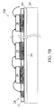
- FIG. 2C is a schematic cross-sectional view of the light emitting device 200 illustrated in FIG. 2A .
- the patterned first conductive layer 23 may be formed on, for example, an insulating layer 26 of the substrate 20 by a suitable process, which may include but is not limited to one of a deposition, sputtering, electroplating and electroless plating process followed by an etching process.
- the patterned second conductive layer 24 may be formed on the patterned first conductive layer 23 by a similar process.
- the light emitting chips 28 may then be attached to the first pads 241 of the patterned second conductive layer 24 by a die attaching process. Subsequently, the chips 28 may be electrically connected to the second pads 242 of the patterned second conductive layer 24 by a wire bonding process.
- Light radiated by the light emitting device 200 may include light emitted from the light emitting chips 28 and light reflected by the patterned first conductive layer 23.
- the relatively high reflective material in the first reflecting units 231 and the second reflecting units 232 of the patterned first conductive layer 23 may facilitate radiation and reflection of light, as shown in broad arrows.
- FIG. 3A is a schematic plan view of a light emitting device 300 in accordance with another example of the present invention.
- the light emitting device 300 may be similar to the light emitting device 200 described and illustrated with reference to FIG. 2A except that, for example, "vertical" chips" 38 replace the lateral chips 28.
- FIG. 3B is a schematic perspective view of the light emitting chip 38 illustrated in FIG. 3A .
- the chip 38 may include a conductive base 392, a p-type doped layer 382 on or over the conductive base 392, an n-type doped layer 381 over the p-type doped layer 382, an active layer 383 between the p-type doped layer 382 and the n-type doped layer 381, and a first electrode 391.
- the n-type doped layer 381 which may include n-type GaN or a combination of undoped GaN and n-GaN, may be deposited on a sacrifice substrate (not shown).
- the active layer 383 to serve as a multiple quantum well may be grown on the n-type doped layer 381.
- the p-type doped layer 382, which may include p-GaN, may be deposited on the active layer 383.
- a reflecting layer 385 may optionally be formed on the p-type doped layer 382.
- the reflecting layer 385 may prevent photons from traveling beyond the semiconductor layers 381, 382 and 383 and into the conductive base 392 for absorption.
- the conductive base 392 which may include a thick metal layer, may be formed on the reflecting layer 385 (if it is present) or on the p-type doped layer 382 (if the reflecting layer 385 is not present).
- the conductive base 392 may serve as a second electrode for the chip 38. Accordingly, current may flow vertically from the second electrode 392 via the active layer 383 toward the first electrode 391.
- an additional conductive layer 386 may be added onto the conductive base 392 to improve the contact resistance and the p-electrode integrity. Subsequently, the sacrifice substrate may be removed, the entire structure is flipped, and the first electrode 391 may then be formed on the n-type doped layer 381.
- the chips 38 may be electrically interconnected by wires 37 in a fashion that the first electrode 391 of one chip such as an exemplary chip 38-1 is coupled via wire 37 to the second electrode 392 of another chip (in the current example a previous chip), and the second electrode 392 of the exemplary chip 38-1 is coupled to the first electrode 391 of yet another chip (in the current example a subsequent chip).
- FIG. 3C is a schematic cross-sectional view of the light emitting device 300 illustrated in FIG. 3A .
- wire 37 that electrically interconnects two adjacent chips 38 may include one end bonded to the first electrode 391 of one of the two chips 38 and the other end bonded to a point 390 on the first pad 241 electrically coupled with the second electrode 392 of the other one of the two chips 38.
- FIG. 4A is a schematic plan view of a light emitting device 400 in accordance with still another example of the present invention.
- the light emitting device 400 may be similar to the light emitting device 200 described and illustrated with reference to FIG. 2A except that, for example, a reflective layer 33 may be formed on the patterned first conductive layer 23 in a reflective region 30 defined by the first and second regions 21 and 22.
- FIG. 4B is a schematic cross-sectional view of the light emitting device 400 illustrated in FIG. 4A .
- the reflective layer 33 may be formed on the patterned first conductive layer 23 by, for example, a coating process, exposing the first pads 241 and the second pads 242 of the patterned second conductive layer 24.
- the reflective layer 33 may include a material of a relatively high reflectivity.
- the reflective layer 33 may include one of magnesium oxide (MgO) and barium sulfate (BaSO 2 ), whose reflectivity may be 90% or more.
- the reflective layer 33 of MgO or BaSO 2 may raise the total reflectivity of the light emitting device from approximately 70% to 80%.
- lateral chips 28 are illustrated as an example, skilled persons in the art will understand that the light emitting device 400 may also be applicable to vertical chips 38 described and illustrated with reference to FIG. 3B .
- FIG. 5A is a schematic plan view of a light emitting device 500 in accordance with yet another example of the present invention.
- the light emitting device 500 may be similar to the light emitting device 400 described and illustrated with reference to FIG. 4A except that, for example, the patterned first conductive layer 23 in the light emitting device 400 may be removed.
- FIG. 5B is a schematic cross-sectional view of the light emitting device 500 illustrated in FIG. 5A .
- the patterned second conductive layer 24 may be formed on the insulating layer 26.
- the reflective layer 33 may be formed on the insulating layer 26, exposing the first and second pads 241 and 242 of the patterned second conductive layer 24. Accordingly, the reflective layer 33 may serve as a reflective region for the light emitting device 500.
- lateral chips 28 are illustrated as an example, skilled persons in the art will understand that the light emitting device 500 may also be applicable to vertical chips 38 described and illustrated with reference to FIG. 3B .
- the specification may have presented the method and/or process of the present invention as a particular sequence of steps. However, to the extent that the method or process does not rely on the particular order of steps set forth herein, the method or process should not be limited to the particular sequence of steps described. As one of ordinary skill in the art would appreciate, other sequences of steps may be possible. Therefore, the particular order of the steps set forth in the specification should not be construed as limitations on the claims. In addition, the claims directed to the method and/or process of the present invention should not be limited to the performance of their steps in the order written, and one skilled in the art can readily appreciate that the sequences may be varied and still remain within the spirit and scope of the present invention.
Landscapes
- Engineering & Computer Science (AREA)
- Microelectronics & Electronic Packaging (AREA)
- Led Devices (AREA)
- Led Device Packages (AREA)
- Parts Printed On Printed Circuit Boards (AREA)
Applications Claiming Priority (1)
| Application Number | Priority Date | Filing Date | Title |
|---|---|---|---|
| US12/768,679 US20110261847A1 (en) | 2010-04-27 | 2010-04-27 | Light emitting devices |
Publications (1)
| Publication Number | Publication Date |
|---|---|
| EP2383780A1 true EP2383780A1 (de) | 2011-11-02 |
Family
ID=44281102
Family Applications (1)
| Application Number | Title | Priority Date | Filing Date |
|---|---|---|---|
| EP20100172281 Withdrawn EP2383780A1 (de) | 2010-04-27 | 2010-08-09 | Lichtemittierende Vorrichtungen |
Country Status (6)
| Country | Link |
|---|---|
| US (1) | US20110261847A1 (de) |
| EP (1) | EP2383780A1 (de) |
| JP (1) | JP2011233856A (de) |
| KR (1) | KR20110119496A (de) |
| CN (1) | CN102237349B (de) |
| TW (1) | TW201138162A (de) |
Cited By (1)
| Publication number | Priority date | Publication date | Assignee | Title |
|---|---|---|---|---|
| EP2927970A4 (de) * | 2012-12-03 | 2016-06-29 | Citizen Holdings Co Ltd | Led-modul |
Families Citing this family (3)
| Publication number | Priority date | Publication date | Assignee | Title |
|---|---|---|---|---|
| US9166372B1 (en) | 2013-06-28 | 2015-10-20 | Soraa Laser Diode, Inc. | Gallium nitride containing laser device configured on a patterned substrate |
| KR102590229B1 (ko) | 2018-10-15 | 2023-10-17 | 삼성전자주식회사 | Led 소자 및 led 소자의 제조 방법 |
| TWI800153B (zh) * | 2020-12-24 | 2023-04-21 | 南韓商東友精細化工有限公司 | 電路板 |
Citations (6)
| Publication number | Priority date | Publication date | Assignee | Title |
|---|---|---|---|---|
| US4424408A (en) * | 1979-11-21 | 1984-01-03 | Elarde Vito D | High temperature circuit board |
| US20030178627A1 (en) * | 2000-10-16 | 2003-09-25 | Werner Marchl | Led module |
| US20080100772A1 (en) * | 2006-11-01 | 2008-05-01 | Au Optronics Corporation | Reflective Light Source Device and Manufacture Method Thereof |
| US20090165296A1 (en) * | 2006-04-04 | 2009-07-02 | Yoash Carmi | Patterns of conductive objects on a substrate and method of producing thereof |
| WO2009145109A1 (ja) * | 2008-05-29 | 2009-12-03 | 電気化学工業株式会社 | 金属ベース回路基板 |
| WO2010038673A1 (ja) * | 2008-09-30 | 2010-04-08 | 日立化成工業株式会社 | コート剤、これを用いた光半導体素子搭載用基板及び光半導体装置 |
Family Cites Families (10)
| Publication number | Priority date | Publication date | Assignee | Title |
|---|---|---|---|---|
| JPH05190899A (ja) * | 1992-01-14 | 1993-07-30 | Rohm Co Ltd | 半導体素子アレイチップ及びその製造方法 |
| JP3431038B2 (ja) * | 1994-02-18 | 2003-07-28 | ローム株式会社 | 発光装置とその製造方法およびledヘッドの製造方法 |
| JPH11216897A (ja) * | 1998-01-30 | 1999-08-10 | Ricoh Co Ltd | 光学装置 |
| JP3795298B2 (ja) * | 2000-03-31 | 2006-07-12 | 豊田合成株式会社 | Iii族窒化物系化合物半導体発光素子の製造方法 |
| JP2006294782A (ja) * | 2005-04-08 | 2006-10-26 | Hitachi Ltd | 半導体光源装置 |
| JP5045166B2 (ja) * | 2007-03-16 | 2012-10-10 | ソニー株式会社 | 光源装置及び液晶表示装置 |
| JP5132234B2 (ja) * | 2007-09-25 | 2013-01-30 | 三洋電機株式会社 | 発光モジュール |
| JP2009167338A (ja) * | 2008-01-18 | 2009-07-30 | Sharp Corp | 波長変換部材およびこれを備える発光装置、ならびに蛍光体 |
| JP2009283832A (ja) * | 2008-05-26 | 2009-12-03 | Rohm Co Ltd | Ledランプ |
| KR101332794B1 (ko) * | 2008-08-05 | 2013-11-25 | 삼성전자주식회사 | 발광 장치, 이를 포함하는 발광 시스템, 상기 발광 장치 및발광 시스템의 제조 방법 |
-
2010
- 2010-04-27 US US12/768,679 patent/US20110261847A1/en not_active Abandoned
- 2010-07-07 TW TW099122317A patent/TW201138162A/zh unknown
- 2010-07-13 JP JP2010159101A patent/JP2011233856A/ja active Pending
- 2010-07-28 KR KR1020100072965A patent/KR20110119496A/ko not_active Ceased
- 2010-08-09 EP EP20100172281 patent/EP2383780A1/de not_active Withdrawn
- 2010-08-16 CN CN201010257692XA patent/CN102237349B/zh active Active
Patent Citations (6)
| Publication number | Priority date | Publication date | Assignee | Title |
|---|---|---|---|---|
| US4424408A (en) * | 1979-11-21 | 1984-01-03 | Elarde Vito D | High temperature circuit board |
| US20030178627A1 (en) * | 2000-10-16 | 2003-09-25 | Werner Marchl | Led module |
| US20090165296A1 (en) * | 2006-04-04 | 2009-07-02 | Yoash Carmi | Patterns of conductive objects on a substrate and method of producing thereof |
| US20080100772A1 (en) * | 2006-11-01 | 2008-05-01 | Au Optronics Corporation | Reflective Light Source Device and Manufacture Method Thereof |
| WO2009145109A1 (ja) * | 2008-05-29 | 2009-12-03 | 電気化学工業株式会社 | 金属ベース回路基板 |
| WO2010038673A1 (ja) * | 2008-09-30 | 2010-04-08 | 日立化成工業株式会社 | コート剤、これを用いた光半導体素子搭載用基板及び光半導体装置 |
Cited By (2)
| Publication number | Priority date | Publication date | Assignee | Title |
|---|---|---|---|---|
| EP2927970A4 (de) * | 2012-12-03 | 2016-06-29 | Citizen Holdings Co Ltd | Led-modul |
| US9810381B2 (en) | 2012-12-03 | 2017-11-07 | Citizen Watch Co., Ltd. | LED module |
Also Published As
| Publication number | Publication date |
|---|---|
| TW201138162A (en) | 2011-11-01 |
| CN102237349B (zh) | 2013-05-29 |
| CN102237349A (zh) | 2011-11-09 |
| US20110261847A1 (en) | 2011-10-27 |
| JP2011233856A (ja) | 2011-11-17 |
| KR20110119496A (ko) | 2011-11-02 |
Similar Documents
| Publication | Publication Date | Title |
|---|---|---|
| KR100694784B1 (ko) | 다층 코팅으로 형성한 플립칩 전극 발광 소자 | |
| JP5432234B2 (ja) | 半導体発光デバイス用の実装 | |
| US9397266B2 (en) | Lateral semiconductor light emitting diodes having large area contacts | |
| JP6101001B2 (ja) | 発光素子パッケージ及びこれを具備した照明システム | |
| JP3130292B2 (ja) | 半導体発光装置及びその製造方法 | |
| TWI580083B (zh) | 發光裝置封裝件 | |
| US7589351B2 (en) | Light-emitting device | |
| US20150188011A1 (en) | Side-emitting type nitride semiconductor light emitting chip and nitride semiconductor light emitting device having the same | |
| JP5693375B2 (ja) | 半導体発光素子 | |
| EP2565944A2 (de) | Lichtemittierendes Halbleiterbauelement | |
| US8754430B2 (en) | Light emitting device and light emitting device package | |
| TWI496324B (zh) | 發光二極體封裝體 | |
| KR100990122B1 (ko) | 교류 발광 다이오드 칩 및 그의 제조방법 | |
| EP2383780A1 (de) | Lichtemittierende Vorrichtungen | |
| KR20160065349A (ko) | 질화물 반도체 발광 칩 및 이를 갖는 발광 소자 | |
| JP4622426B2 (ja) | 半導体発光素子 | |
| CN101752466B (zh) | 发光组件 | |
| TWI473299B (zh) | 覆晶式發光二極體及其製法與應用 | |
| CN102610726A (zh) | 发光组件 | |
| CN100383992C (zh) | 发光二极管及其制造方法 | |
| KR102459096B1 (ko) | 발광 소자 패키지 및 이의 제조 방법 | |
| JP6940739B2 (ja) | 発光素子及び発光素子の製造方法 | |
| TW200411950A (en) | High-luminance light-emitting device |
Legal Events
| Date | Code | Title | Description |
|---|---|---|---|
| AK | Designated contracting states |
Kind code of ref document: A1 Designated state(s): AL AT BE BG CH CY CZ DE DK EE ES FI FR GB GR HR HU IE IS IT LI LT LU LV MC MK MT NL NO PL PT RO SE SI SK SM TR |
|
| AX | Request for extension of the european patent |
Extension state: BA ME RS |
|
| PUAI | Public reference made under article 153(3) epc to a published international application that has entered the european phase |
Free format text: ORIGINAL CODE: 0009012 |
|
| 17P | Request for examination filed |
Effective date: 20120308 |
|
| RAP1 | Party data changed (applicant data changed or rights of an application transferred) |
Owner name: INTERLIGHT OPTOTECH CORPORATION |
|
| 17Q | First examination report despatched |
Effective date: 20150508 |
|
| STAA | Information on the status of an ep patent application or granted ep patent |
Free format text: STATUS: THE APPLICATION IS DEEMED TO BE WITHDRAWN |
|
| 18D | Application deemed to be withdrawn |
Effective date: 20160622 |