EP2383860B1 - Appareil de chargement rapide - Google Patents
Appareil de chargement rapide Download PDFInfo
- Publication number
- EP2383860B1 EP2383860B1 EP10166784.8A EP10166784A EP2383860B1 EP 2383860 B1 EP2383860 B1 EP 2383860B1 EP 10166784 A EP10166784 A EP 10166784A EP 2383860 B1 EP2383860 B1 EP 2383860B1
- Authority
- EP
- European Patent Office
- Prior art keywords
- voltage
- rapid charging
- connection
- connection unit
- terminal
- Prior art date
- Legal status (The legal status is an assumption and is not a legal conclusion. Google has not performed a legal analysis and makes no representation as to the accuracy of the status listed.)
- Active
Links
Images

Classifications
-
- H—ELECTRICITY
- H02—GENERATION; CONVERSION OR DISTRIBUTION OF ELECTRIC POWER
- H02J—ELECTRIC POWER NETWORKS; CIRCUIT ARRANGEMENTS OR SYSTEMS FOR SUPPLYING OR DISTRIBUTING ELECTRIC POWER; SYSTEMS FOR STORING ELECTRIC ENERGY
- H02J7/00—Circuit arrangements for charging or discharging batteries or for supplying loads from batteries
-
- G—PHYSICS
- G06—COMPUTING OR CALCULATING; COUNTING
- G06F—ELECTRIC DIGITAL DATA PROCESSING
- G06F1/00—Details not covered by groups G06F3/00 - G06F13/00 and G06F21/00
- G06F1/26—Power supply means, e.g. regulation thereof
- G06F1/266—Arrangements to supply power to external peripherals either directly from the computer or under computer control, e.g. supply of power through the communication port, computer controlled power-strips
-
- H—ELECTRICITY
- H02—GENERATION; CONVERSION OR DISTRIBUTION OF ELECTRIC POWER
- H02J—ELECTRIC POWER NETWORKS; CIRCUIT ARRANGEMENTS OR SYSTEMS FOR SUPPLYING OR DISTRIBUTING ELECTRIC POWER; SYSTEMS FOR STORING ELECTRIC ENERGY
- H02J1/00—Circuit arrangements for DC mains or DC distribution networks
- H02J1/08—Three-wire DC power distribution systems; Systems having more than three wires
- H02J1/082—DC supplies with two or more different DC voltage levels
-
- G—PHYSICS
- G06—COMPUTING OR CALCULATING; COUNTING
- G06F—ELECTRIC DIGITAL DATA PROCESSING
- G06F2213/00—Indexing scheme relating to interconnection of, or transfer of information or other signals between, memories, input/output devices or central processing units
- G06F2213/38—Universal adapter
- G06F2213/3812—USB port controller
-
- H—ELECTRICITY
- H02—GENERATION; CONVERSION OR DISTRIBUTION OF ELECTRIC POWER
- H02J—ELECTRIC POWER NETWORKS; CIRCUIT ARRANGEMENTS OR SYSTEMS FOR SUPPLYING OR DISTRIBUTING ELECTRIC POWER; SYSTEMS FOR STORING ELECTRIC ENERGY
- H02J2207/00—Details of circuit arrangements for charging or discharging batteries or supplying loads from batteries
- H02J2207/20—Charging or discharging characterised by the power electronics converter
-
- H—ELECTRICITY
- H02—GENERATION; CONVERSION OR DISTRIBUTION OF ELECTRIC POWER
- H02J—ELECTRIC POWER NETWORKS; CIRCUIT ARRANGEMENTS OR SYSTEMS FOR SUPPLYING OR DISTRIBUTING ELECTRIC POWER; SYSTEMS FOR STORING ELECTRIC ENERGY
- H02J2207/00—Details of circuit arrangements for charging or discharging batteries or supplying loads from batteries
- H02J2207/30—Charge provided using DC bus or data bus of a computer
Definitions
- the invention relates generally to a rapid charging apparatus, and more particularly, to a rapid charging apparatus of an electronic device.
- connection port can be a Universal Serial Bus (USB) connection port, for example. While data transfer occurs between the smartphone and the personal computer, the smartphone can charge a battery therein through the connection port receiving a power from the personal computer.
- USB Universal Serial Bus
- the multimedia devices can connect with the personal computer to receive data therefrom, or to transfer data to the personal computer.
- Data can be transferred back and forth between the multimedia devices and the personal computer through a connective line to a connection port of the personal computer, in which the connection port can be a USB connection port, for instance.
- the connection port can be a USB connection port, for instance. While data transfer occurs between the multimedia devices and the personal computer, some multimedia devices can charge a battery therein through the connection port receiving a power from the personal computer.
- EP 1487081A2 it is disclosed a system and methods for charging a rechargeable power source in a mobile device through a USB port.
- the USB charger includes a power converter, a signal generator and a USB connector.
- USB specification which regulates the standard of the electrical of the USB 2.0.
- US 2009/119 520 A1 discloses an information processing apparatus having a function of charging an externally connected peripheral device.
- the external device which is capable of being charged from a USB port and there is an external device which can be charged rapidly and there is an external device which can be charged only at a normal speed.
- the apparatus includes a USB port made to be able to switch a USB charge control signal to LOW (voltage) or HIGH voltage.
- An aspect of the invention provides a rapid charging apparatus capable of turning on a rapid charging function of an electronic device.
- An aspect of the invention provides a rapid charging apparatus including a first connection unit, a second connection unit, and a rapid charging power transformation unit.
- the first connection unit is connectable to a connector for receiving a power.
- the rapid charging power transformation unit is coupled to the first connection unit to receive a voltage of the connector and to provide a first voltage and a second voltage.
- the first voltage ranges from 3.2 V to 1.1 V
- the second voltage ranges from 2.7 V to 0.6 V
- a voltage difference between the first voltage and the second voltage ranges from 0.5 V to 0.8 V.
- the second connection unit is connectable to the electronic device and the rapid charging power transformation unit, so as to transmit the first voltage and the second voltage to the electronic device, whereby the first voltage and the second voltage can turn on a rapid charging function of the electronic device.
- the rapid charging apparatus further comprises a switch having an input terminal, a first connection terminal, and a second connection terminal, wherein the input terminal is coupled to the first connection unit, the first connection terminal is coupled to the second connection unit, and the second connection terminal is coupled to the rapid charging transformation unit.
- the rapid charging power transformation unit includes a first resistor, a second resistor, a third resistor, and a fourth resistor.
- the first resistor has a first terminal coupled to the voltage of the connector, and a second terminal outputting the first voltage.
- the second resistor has a first terminal coupled to the second terminal of the first resistor, and a second terminal coupled to a ground voltage.
- the third resistor has a first terminal coupled to the voltage of the connector, and a second terminal outputting the second voltage.
- the fourth resistor has a first terminal coupled to the second terminal of the third resistor, and a second terminal coupled to the ground voltage.
- the first connection unit is a Universal Serial Bus (USB) plug
- the second connection unit is a USB connection port
- the first voltage and the second voltage are respectively transmitted to the electronic device through a first data pin and a second data pin of the second connection unit.
- the first connection unit is an IEEE 1394 plug
- the second connection unit is a USB connection port
- the first connection unit and the second connection unit are respectively a plug having a transfer power or a connection port having the transfer power.
- the first connection unit and the second connection unit are connection interfaces of a same type or a same form.
- the first connection unit and the second connection unit are connection interfaces of different types.
- the rapid charging power transformation unit and the rapid charging power turn-on unit thereof provide the first and second voltages which can turn on the rapid charging function of the electronic device (e.g., smartphones or handheld multimedia devices).
- the electronic device receives the first and second voltages such that the rapid charging function thereof is turned on, and thereby accelerating a charging speed of the electronic device.
- FIG. 1 is a system block diagram of a rapid charging apparatus in accordance with an embodiment of the invention.
- an electronic device 20 may be a smartphone or a handheld multimedia device, in which the smartphone is an iPhone, and the handheld multimedia device is an iPad or an iPod, for example.
- a rapid charging apparatus 100 includes a rapid charging power transformation unit 110, a first connection unit 120, and a second connection unit 130.
- the first connection unit 120 can be a plug which can also be a Universal Serial Bus (USB) plug (e.g., a plug having a transfer power), for plugging into a USB connection port (e.g., a connector with a power) of a mother board 10.
- USB Universal Serial Bus
- the first connection unit 120 is coupled to the mother board 10 to receive a system voltage Vcc (e.g., a voltage of the connector) of the mother board 10.
- the system voltage Vcc can be an operating voltage or a standby voltage of the mother board 10.
- the second connection port 130 can be a connection port which can also be a USB connection port (e.g, a connection port having the transfer power), so as to connect a connective line of the electronic device 20 with the second connection unit 130, and thereby coupling the second connection unit 130 with the electronic device 20.
- the second connection unit 130 is coupled to the first connection unit 120, for transmitting the system voltage Vcc of the mother board 10 to the electronic device 20.
- the rapid charging power transformation unit 110 is coupled to the first connection unit 120 to receive the system voltage Vcc of the mother board 10, and coupled to the second connection unit 130 to provide a first voltage V1 and a second voltage V2 to the electronic device 20.
- the first voltage V1 ranges from 3.2 V to 1.1 V
- the second voltage V2 ranges from 2.7 V to 0.6 V
- a voltage difference between the first voltage V1 and the second voltage V2 ranges from 0.5 V to 0.8 V.
- the first voltage V1 and the second voltage V2 can turn on a rapid charging function of the electronic device 20.
- the first voltage V1 of the rapid charging power transformation unit 110 is transmitted to a first data pin DP 1 of the second connection unit 130, so as to transmit the first voltage V1 to the electronic device 20 through the first data pin DP1.
- the second voltage V2 of the rapid charging power transformation unit 110 is transmitted to a second data pin DP2 of the second connection unit 130, so as to transmit the second voltage V2 to the electronic device 20 through the second data pin DP2.
- the first data pin DP1 can be a positive data pin (D+) of the USB connection port
- the second data pin DP2 can be a negative data pin (D-) of the USB connection port.
- the electronic device 20 when the electronic device 20 is coupled to the mother board 10 through the rapid charging apparatus 100, the electronic device 20 receives the first voltage V1 and the second voltage V2 provided by the rapid charging power transformation unit 110, and the electronic device 20 receives the system voltage Vcc of the mother board 10 through the first connection unit 120 and the second connection unit 130. At this moment, the electronic device 20 is controlled by the first voltage V1 and the second voltage V2 to turn on a rapid charging function thereof, such that the electronic device 20 can receive the system voltage Vcc of the mother board 100 to perform rapid battery charging.
- the afore-described embodiment exemplifies the power providing device with the mother board.
- electronic devices having USB connection ports may also be used as power providing devices, for instance chargers or power suppliers having USB connection ports.
- the first connection unit 120 may also be an IEEE 1394 plug, adapted for coupling to an IEEE 1394 connection port of the mother board 10, thereby receiving the system voltage Vcc of the mother board 10.
- the type of the second connection unit 130 may be altered according to the plug of the connective line of the electronic device 20.
- first connection unit 120 and the second connection unit 130 may be connection interfaces of a same type (e.g., USB or IEEE 1394) or a same form (e.g., plugs or connection ports), or connection interfaces of different types or different forms, as may be stipulated by a design requirement.
- a same type e.g., USB or IEEE 1394
- a same form e.g., plugs or connection ports
- connection interfaces of different types or different forms as may be stipulated by a design requirement.
- FIG. 2 is a circuit diagram of the rapid charging power transformation unit depicted in FIG. 1 .
- the rapid charging power transformation unit 130 includes a first resistor R1, a second resistor R2, a third resistor R3, and a fourth resistor R4.
- the first resistor R1 has a first terminal coupled to the system voltage Vcc, and a second terminal outputting the first voltage V1.
- the second resistor R2 has a first terminal coupled to the second terminal of the first resistor R1, and a second terminal coupled to a ground voltage.
- the third resistor R3 has a first terminal coupled to the system voltage Vcc, and a second terminal outputting the second voltage V2.
- the fourth resistor R4 has a first terminal coupled to the second terminal of the third resistor R3, and a second terminal coupled to the ground voltage.
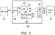
- FIG. 3 is a system block diagram of a rapid charging apparatus in accordance with another embodiment of the invention.
- a difference in the present embodiment resides in a switch 310 and a rapid charging power turn-on unit 320 of a rapid charging apparatus 300.
- the switch 310 has an input terminal 311 coupled to the first connection unit 120 to receive a power (e.g., the system voltage Vcc) therefrom, a first connection terminal 312 coupled to the second connection unit 130 to transmit the system voltage Vcc thereto, and a second connection terminal 313 coupled to the rapid charging power turn-on unit 320 to determine whether to transmit the system voltage Vcc thereto.
- a power e.g., the system voltage Vcc
- the rapid charging power turn-on unit 320 When the rapid charging power turn-on unit 320 receives the system voltage Vcc, the first voltage V1 and the second voltage V2 are provided by using the system voltage Vcc, and the first and second voltages V1 and V2 are transmitted to the second connection unit 130. At this moment, the first and second voltages V1 and V2 are transmitted to the electronic device 20 to turn on the rapid charging function thereof through the second connection unit 130, such that the electronic device 20 rapidly charges a battery thereof by using the system voltage Vcc. Since the circuit structure of the rapid charging power turn-on unit 320 is similar to that of the rapid charging power transformation unit 110, further description is omitted hereafter.
- the rapid charging power transformation unit and the rapid charging power turn-on unit thereof provide the first and second voltages which can turn on the rapid charging function of the electronic device (e.g., smartphones or handheld multimedia devices).
- the electronic device When the electronic device is coupled to the connector of the mother board (or a connector of another electronic device) through the rapid charging apparatus, the electronic device receives the first and second voltages such that the rapid charging function thereof is turned on, and thereby accelerating a charging speed of the electronic device.
Landscapes
- Engineering & Computer Science (AREA)
- Power Engineering (AREA)
- General Engineering & Computer Science (AREA)
- Theoretical Computer Science (AREA)
- Computer Hardware Design (AREA)
- Physics & Mathematics (AREA)
- General Physics & Mathematics (AREA)
- Charge And Discharge Circuits For Batteries Or The Like (AREA)
- Secondary Cells (AREA)
- Power Sources (AREA)
Claims (9)
- Appareil de charge rapide (100), comprenant :une première unité de connexion (120), connectable à un connecteur pour recevoir de l'énergie ;une unité de transformation d'énergie de charge rapide (110), couplée à la première unité de connexion (120) pour recevoir une tension du connecteur et pour fournir une première tension et une deuxième tension, dans lequel la première tension est comprise entre 3,2 V et 1,1 V, la deuxième tension est comprise entre 2,7 V et 0,6 V, et la différence de tension entre la première tension et la deuxième tension est comprise entre 0,5 V et 0,8 V ; etune deuxième unité de connexion (130), connectable à un dispositif électronique (20) et à l'unité de transformation d'énergie de charge rapide (110) de manière à transmettre la première tension et la deuxième tension au dispositif électronique (20), moyennant quoi la première tension et la deuxième tension peuvent activer une fonction de charge rapide du dispositif électronique.
- Appareil de charge rapide (100) selon la revendication 1, caractérisé en ce qu'il comprend en outre un interrupteur (310) qui comporte une borne d'entrée (311), une première borne de connexion (312), et une deuxième borne de connexion (313), dans lequel la borne d'entrée (311) est couplée à la première unité de connexion (120), la première borne de connexion (312) est couplée à la deuxième unité de connexion (130), et la deuxième borne de connexion (313) est couplée à l'unité de transformation de charge rapide (110) .
- Appareil de charge rapide (100) selon la revendication 1 ou 2, caractérisé en ce que l'unité de transformation d'énergie de charge rapide (110) comprend :une première résistance (R1) comportant une première borne couplée à la tension du connecteur, et une deuxième borne sortant la première tension ;une deuxième résistance (R2) comportant une première borne couplée à la deuxième borne de la première résistance, et une deuxième borne couplée à une tension de terre ;une troisième résistance (R3) comportant une première borne couplée à la tension du connecteur, et une deuxième borne sortant la deuxième tension ; etune quatrième résistance (R4) comportant une première borne couplée à la deuxième borne de la troisième résistance (R3), et une deuxième borne couplée à la tension de terre.
- Appareil de charge rapide (100) selon la revendication 1 ou 2, caractérisé en ce que la première unité de connexion (120) est une prise de bus universel en série (USB), et la deuxième unité de connexion (130) est un port de connexion USB.
- Appareil de charge rapide (100) selon la revendication 4, caractérisé en ce que la première tension et la deuxième tension sont transmises respectivement au dispositif électronique (20) via une première broche de données et une deuxième broche de données de la deuxième unité de connexion (130).
- Appareil de charge rapide (100) selon la revendication 1 ou 2, caractérisé en ce que la première unité de connexion (120) est une prise IEEE 1394, et la deuxième unité de connexion (130) est un port de connexion USB.
- Appareil de charge rapide (100) selon la revendication 1 ou 2, caractérisé en ce que la première unité de connexion (120) et la deuxième unité de connexion (130) sont respectivement une prise ayant une puissance de transfert ou un port de connexion ayant la puissance de transfert.
- Appareil de charge rapide (100) selon la revendication 7, caractérisé en ce que la première unité de connexion (120) et la deuxième unité de connexion (130) sont des interfaces connectables d'un même type et d'une même forme.
- Appareil de charge rapide (100) selon la revendication 8, caractérisé en ce que la première unité de connexion (120) et la deuxième unité de connexion (130) sont des interfaces connectables de différents types.
Applications Claiming Priority (2)
| Application Number | Priority Date | Filing Date | Title |
|---|---|---|---|
| TW099113697A TWI495224B (zh) | 2010-04-29 | 2010-04-29 | 智慧型手機的快充裝置 |
| TW99115508A TWI399009B (zh) | 2010-05-14 | 2010-05-14 | 手持式多媒體裝置的快充裝置 |
Publications (3)
| Publication Number | Publication Date |
|---|---|
| EP2383860A2 EP2383860A2 (fr) | 2011-11-02 |
| EP2383860A3 EP2383860A3 (fr) | 2016-04-06 |
| EP2383860B1 true EP2383860B1 (fr) | 2019-11-27 |
Family
ID=44501760
Family Applications (1)
| Application Number | Title | Priority Date | Filing Date |
|---|---|---|---|
| EP10166784.8A Active EP2383860B1 (fr) | 2010-04-29 | 2010-06-22 | Appareil de chargement rapide |
Country Status (3)
| Country | Link |
|---|---|
| US (1) | US20110269513A1 (fr) |
| EP (1) | EP2383860B1 (fr) |
| JP (1) | JP2011233129A (fr) |
Families Citing this family (4)
| Publication number | Priority date | Publication date | Assignee | Title |
|---|---|---|---|---|
| US9077756B1 (en) * | 2012-03-05 | 2015-07-07 | Symantec Corporation | Limiting external device access to mobile computing devices according to device type and connection context |
| JP6488733B2 (ja) | 2015-02-02 | 2019-03-27 | 株式会社ソシオネクスト | 電源回路、充電回路、充電システム、給電方法及び充電方法 |
| KR102508958B1 (ko) | 2016-10-06 | 2023-03-13 | 삼성전자주식회사 | 충전을 수행하는 전자 장치 및 그 제어 방법 |
| US11005275B2 (en) | 2018-01-26 | 2021-05-11 | Wbtec, Llc | Intelligent charging USB splitter |
Citations (1)
| Publication number | Priority date | Publication date | Assignee | Title |
|---|---|---|---|---|
| US20090119520A1 (en) * | 2007-11-07 | 2009-05-07 | Kabushiki Kaisha Toshiba | Information processing apparatus |
Family Cites Families (11)
| Publication number | Priority date | Publication date | Assignee | Title |
|---|---|---|---|---|
| GB2262170B (en) * | 1991-12-05 | 1995-04-12 | Mitac Int Corp | Internal card type uninterruptible power system |
| US7376846B2 (en) * | 2001-10-14 | 2008-05-20 | Palm, Inc. | Charging and communication cable system for a mobile computer apparatus |
| JP2003217685A (ja) * | 2002-01-28 | 2003-07-31 | Nec Infrontia Corp | バッテリパック |
| JP2003345467A (ja) * | 2002-05-28 | 2003-12-05 | Nec Corp | 情報処理装置 |
| GB2402819B (en) * | 2003-06-11 | 2005-08-03 | Research In Motion Ltd | Universal serial bus charger for a mobile device |
| US7581119B2 (en) * | 2004-07-18 | 2009-08-25 | Apple Inc. | Method and system for discovering a power source on a peripheral bus |
| JP2007011551A (ja) * | 2005-06-29 | 2007-01-18 | Nobuyuki Suzuki | 電力供給装置 |
| JP2007068333A (ja) * | 2005-08-31 | 2007-03-15 | Sony Corp | 電源供給専用装置,端末,電源供給システム,および電源供給方法 |
| US20080265838A1 (en) * | 2007-04-24 | 2008-10-30 | Saurabh Garg | Battery charging using a USB-ID pin of a USB interface |
| WO2009031235A1 (fr) * | 2007-09-07 | 2009-03-12 | Fujitsu Limited | Appareil de traitement de l'information et circuit de commande de flux |
| US8847549B2 (en) * | 2008-09-30 | 2014-09-30 | Tarah Graham | Docking stations for remote control and multimedia devices |
-
2010
- 2010-06-22 EP EP10166784.8A patent/EP2383860B1/fr active Active
- 2010-07-14 US US12/835,760 patent/US20110269513A1/en not_active Abandoned
- 2010-10-14 JP JP2010231871A patent/JP2011233129A/ja active Pending
Patent Citations (1)
| Publication number | Priority date | Publication date | Assignee | Title |
|---|---|---|---|---|
| US20090119520A1 (en) * | 2007-11-07 | 2009-05-07 | Kabushiki Kaisha Toshiba | Information processing apparatus |
Also Published As
| Publication number | Publication date |
|---|---|
| JP2011233129A (ja) | 2011-11-17 |
| EP2383860A2 (fr) | 2011-11-02 |
| US20110269513A1 (en) | 2011-11-03 |
| EP2383860A3 (fr) | 2016-04-06 |
Similar Documents
| Publication | Publication Date | Title |
|---|---|---|
| CN108718020B (zh) | 集线器 | |
| CN107465240B (zh) | 一种智能移动电源及与其进行usb数据通讯的方法 | |
| US10998737B2 (en) | Intelligent switch system | |
| EP2387125A2 (fr) | Carte mère avec dispositif multimédia portable à chargement rapide | |
| EP3490100A1 (fr) | Système de charge, terminal, adaptateur d'alimentation et ligne de charge | |
| CN105324911A (zh) | 充电装置及其操作方法 | |
| EP2383860B1 (fr) | Appareil de chargement rapide | |
| CN102270860B (zh) | 智能型手机的快充装置 | |
| CN113535622B (zh) | 供电切换系统、usb插座和电子设备 | |
| US8463978B2 (en) | Computer with ability to charge electronic device in power off state and USB interface module thereof | |
| CN206162505U (zh) | 一种双usb接口电路 | |
| US20140344493A1 (en) | Usb interface detection device | |
| CN203520878U (zh) | 多功能u盘 | |
| CN201075214Y (zh) | 一种usb通用数据线 | |
| CN207518016U (zh) | 无线充电转接电路及装置 | |
| CN107706977A (zh) | 一种充电电流的检测方法以及充电装置 | |
| CN204067514U (zh) | 一种激活电池的装置、终端、充电器及系统 | |
| CN102236374B (zh) | 主机板 | |
| CN102544919A (zh) | 电缆 | |
| CN204706725U (zh) | 一种充电数据线 | |
| CN109218880A (zh) | 耳机充电二合一电路及控制方法、终端 | |
| CN209401012U (zh) | 一种usb接口电源控制装置 | |
| TWI495224B (zh) | 智慧型手機的快充裝置 | |
| CN201956711U (zh) | 用于向待充电设备提供充电服务的平台 | |
| EP2381368A1 (fr) | Carte mère dotée d'une option de charge rapide de batterie dans une port de connexion |
Legal Events
| Date | Code | Title | Description |
|---|---|---|---|
| AK | Designated contracting states |
Kind code of ref document: A2 Designated state(s): AL AT BE BG CH CY CZ DE DK EE ES FI FR GB GR HR HU IE IS IT LI LT LU LV MC MK MT NL NO PL PT RO SE SI SK SM TR |
|
| AX | Request for extension of the european patent |
Extension state: BA ME RS |
|
| PUAI | Public reference made under article 153(3) epc to a published international application that has entered the european phase |
Free format text: ORIGINAL CODE: 0009012 |
|
| RAP1 | Party data changed (applicant data changed or rights of an application transferred) |
Owner name: GIGA-BYTE TECHNOLOGY CO., LTD. |
|
| RIC1 | Information provided on ipc code assigned before grant |
Ipc: H02J 7/00 20060101AFI20151211BHEP Ipc: H02J 1/00 20060101ALI20151211BHEP |
|
| PUAL | Search report despatched |
Free format text: ORIGINAL CODE: 0009013 |
|
| RIC1 | Information provided on ipc code assigned before grant |
Ipc: H02J 1/00 20060101ALI20160225BHEP Ipc: H02J 7/00 20060101AFI20160225BHEP |
|
| AK | Designated contracting states |
Kind code of ref document: A3 Designated state(s): AL AT BE BG CH CY CZ DE DK EE ES FI FR GB GR HR HU IE IS IT LI LT LU LV MC MK MT NL NO PL PT RO SE SI SK SM TR |
|
| AX | Request for extension of the european patent |
Extension state: BA ME RS |
|
| 17P | Request for examination filed |
Effective date: 20161006 |
|
| RBV | Designated contracting states (corrected) |
Designated state(s): AL AT BE BG CH CY CZ DE DK EE ES FI FR GB GR HR HU IE IS IT LI LT LU LV MC MK MT NL NO PL PT RO SE SI SK SM TR |
|
| STAA | Information on the status of an ep patent application or granted ep patent |
Free format text: STATUS: EXAMINATION IS IN PROGRESS |
|
| 17Q | First examination report despatched |
Effective date: 20181023 |
|
| REG | Reference to a national code |
Ref country code: DE Ref legal event code: R079 Ref document number: 602010062113 Country of ref document: DE Free format text: PREVIOUS MAIN CLASS: H02J0007000000 Ipc: G06F0001260000 |
|
| GRAP | Despatch of communication of intention to grant a patent |
Free format text: ORIGINAL CODE: EPIDOSNIGR1 |
|
| STAA | Information on the status of an ep patent application or granted ep patent |
Free format text: STATUS: GRANT OF PATENT IS INTENDED |
|
| RIC1 | Information provided on ipc code assigned before grant |
Ipc: G06F 1/26 20060101AFI20190607BHEP Ipc: H02J 7/00 20060101ALI20190607BHEP Ipc: H02J 1/00 20060101ALI20190607BHEP |
|
| INTG | Intention to grant announced |
Effective date: 20190628 |
|
| GRAS | Grant fee paid |
Free format text: ORIGINAL CODE: EPIDOSNIGR3 |
|
| GRAA | (expected) grant |
Free format text: ORIGINAL CODE: 0009210 |
|
| STAA | Information on the status of an ep patent application or granted ep patent |
Free format text: STATUS: THE PATENT HAS BEEN GRANTED |
|
| AK | Designated contracting states |
Kind code of ref document: B1 Designated state(s): AL AT BE BG CH CY CZ DE DK EE ES FI FR GB GR HR HU IE IS IT LI LT LU LV MC MK MT NL NO PL PT RO SE SI SK SM TR |
|
| REG | Reference to a national code |
Ref country code: GB Ref legal event code: FG4D |
|
| REG | Reference to a national code |
Ref country code: CH Ref legal event code: EP |
|
| REG | Reference to a national code |
Ref country code: AT Ref legal event code: REF Ref document number: 1207415 Country of ref document: AT Kind code of ref document: T Effective date: 20191215 |
|
| REG | Reference to a national code |
Ref country code: DE Ref legal event code: R096 Ref document number: 602010062113 Country of ref document: DE |
|
| REG | Reference to a national code |
Ref country code: IE Ref legal event code: FG4D |
|
| REG | Reference to a national code |
Ref country code: NL Ref legal event code: MP Effective date: 20191127 |
|
| REG | Reference to a national code |
Ref country code: LT Ref legal event code: MG4D |
|
| PG25 | Lapsed in a contracting state [announced via postgrant information from national office to epo] |
Ref country code: FI Free format text: LAPSE BECAUSE OF FAILURE TO SUBMIT A TRANSLATION OF THE DESCRIPTION OR TO PAY THE FEE WITHIN THE PRESCRIBED TIME-LIMIT Effective date: 20191127 Ref country code: BG Free format text: LAPSE BECAUSE OF FAILURE TO SUBMIT A TRANSLATION OF THE DESCRIPTION OR TO PAY THE FEE WITHIN THE PRESCRIBED TIME-LIMIT Effective date: 20200227 Ref country code: NL Free format text: LAPSE BECAUSE OF FAILURE TO SUBMIT A TRANSLATION OF THE DESCRIPTION OR TO PAY THE FEE WITHIN THE PRESCRIBED TIME-LIMIT Effective date: 20191127 Ref country code: LV Free format text: LAPSE BECAUSE OF FAILURE TO SUBMIT A TRANSLATION OF THE DESCRIPTION OR TO PAY THE FEE WITHIN THE PRESCRIBED TIME-LIMIT Effective date: 20191127 Ref country code: SE Free format text: LAPSE BECAUSE OF FAILURE TO SUBMIT A TRANSLATION OF THE DESCRIPTION OR TO PAY THE FEE WITHIN THE PRESCRIBED TIME-LIMIT Effective date: 20191127 Ref country code: ES Free format text: LAPSE BECAUSE OF FAILURE TO SUBMIT A TRANSLATION OF THE DESCRIPTION OR TO PAY THE FEE WITHIN THE PRESCRIBED TIME-LIMIT Effective date: 20191127 Ref country code: NO Free format text: LAPSE BECAUSE OF FAILURE TO SUBMIT A TRANSLATION OF THE DESCRIPTION OR TO PAY THE FEE WITHIN THE PRESCRIBED TIME-LIMIT Effective date: 20200227 Ref country code: GR Free format text: LAPSE BECAUSE OF FAILURE TO SUBMIT A TRANSLATION OF THE DESCRIPTION OR TO PAY THE FEE WITHIN THE PRESCRIBED TIME-LIMIT Effective date: 20200228 Ref country code: LT Free format text: LAPSE BECAUSE OF FAILURE TO SUBMIT A TRANSLATION OF THE DESCRIPTION OR TO PAY THE FEE WITHIN THE PRESCRIBED TIME-LIMIT Effective date: 20191127 |
|
| PG25 | Lapsed in a contracting state [announced via postgrant information from national office to epo] |
Ref country code: IS Free format text: LAPSE BECAUSE OF FAILURE TO SUBMIT A TRANSLATION OF THE DESCRIPTION OR TO PAY THE FEE WITHIN THE PRESCRIBED TIME-LIMIT Effective date: 20200327 Ref country code: HR Free format text: LAPSE BECAUSE OF FAILURE TO SUBMIT A TRANSLATION OF THE DESCRIPTION OR TO PAY THE FEE WITHIN THE PRESCRIBED TIME-LIMIT Effective date: 20191127 |
|
| PG25 | Lapsed in a contracting state [announced via postgrant information from national office to epo] |
Ref country code: AL Free format text: LAPSE BECAUSE OF FAILURE TO SUBMIT A TRANSLATION OF THE DESCRIPTION OR TO PAY THE FEE WITHIN THE PRESCRIBED TIME-LIMIT Effective date: 20191127 |
|
| PG25 | Lapsed in a contracting state [announced via postgrant information from national office to epo] |
Ref country code: DK Free format text: LAPSE BECAUSE OF FAILURE TO SUBMIT A TRANSLATION OF THE DESCRIPTION OR TO PAY THE FEE WITHIN THE PRESCRIBED TIME-LIMIT Effective date: 20191127 Ref country code: PT Free format text: LAPSE BECAUSE OF FAILURE TO SUBMIT A TRANSLATION OF THE DESCRIPTION OR TO PAY THE FEE WITHIN THE PRESCRIBED TIME-LIMIT Effective date: 20200419 Ref country code: EE Free format text: LAPSE BECAUSE OF FAILURE TO SUBMIT A TRANSLATION OF THE DESCRIPTION OR TO PAY THE FEE WITHIN THE PRESCRIBED TIME-LIMIT Effective date: 20191127 Ref country code: RO Free format text: LAPSE BECAUSE OF FAILURE TO SUBMIT A TRANSLATION OF THE DESCRIPTION OR TO PAY THE FEE WITHIN THE PRESCRIBED TIME-LIMIT Effective date: 20191127 Ref country code: CZ Free format text: LAPSE BECAUSE OF FAILURE TO SUBMIT A TRANSLATION OF THE DESCRIPTION OR TO PAY THE FEE WITHIN THE PRESCRIBED TIME-LIMIT Effective date: 20191127 |
|
| REG | Reference to a national code |
Ref country code: DE Ref legal event code: R097 Ref document number: 602010062113 Country of ref document: DE |
|
| PG25 | Lapsed in a contracting state [announced via postgrant information from national office to epo] |
Ref country code: SM Free format text: LAPSE BECAUSE OF FAILURE TO SUBMIT A TRANSLATION OF THE DESCRIPTION OR TO PAY THE FEE WITHIN THE PRESCRIBED TIME-LIMIT Effective date: 20191127 Ref country code: SK Free format text: LAPSE BECAUSE OF FAILURE TO SUBMIT A TRANSLATION OF THE DESCRIPTION OR TO PAY THE FEE WITHIN THE PRESCRIBED TIME-LIMIT Effective date: 20191127 |
|
| REG | Reference to a national code |
Ref country code: AT Ref legal event code: MK05 Ref document number: 1207415 Country of ref document: AT Kind code of ref document: T Effective date: 20191127 |
|
| PLBE | No opposition filed within time limit |
Free format text: ORIGINAL CODE: 0009261 |
|
| STAA | Information on the status of an ep patent application or granted ep patent |
Free format text: STATUS: NO OPPOSITION FILED WITHIN TIME LIMIT |
|
| 26N | No opposition filed |
Effective date: 20200828 |
|
| PG25 | Lapsed in a contracting state [announced via postgrant information from national office to epo] |
Ref country code: AT Free format text: LAPSE BECAUSE OF FAILURE TO SUBMIT A TRANSLATION OF THE DESCRIPTION OR TO PAY THE FEE WITHIN THE PRESCRIBED TIME-LIMIT Effective date: 20191127 Ref country code: PL Free format text: LAPSE BECAUSE OF FAILURE TO SUBMIT A TRANSLATION OF THE DESCRIPTION OR TO PAY THE FEE WITHIN THE PRESCRIBED TIME-LIMIT Effective date: 20191127 Ref country code: SI Free format text: LAPSE BECAUSE OF FAILURE TO SUBMIT A TRANSLATION OF THE DESCRIPTION OR TO PAY THE FEE WITHIN THE PRESCRIBED TIME-LIMIT Effective date: 20191127 |
|
| PG25 | Lapsed in a contracting state [announced via postgrant information from national office to epo] |
Ref country code: IT Free format text: LAPSE BECAUSE OF FAILURE TO SUBMIT A TRANSLATION OF THE DESCRIPTION OR TO PAY THE FEE WITHIN THE PRESCRIBED TIME-LIMIT Effective date: 20191127 Ref country code: MC Free format text: LAPSE BECAUSE OF FAILURE TO SUBMIT A TRANSLATION OF THE DESCRIPTION OR TO PAY THE FEE WITHIN THE PRESCRIBED TIME-LIMIT Effective date: 20191127 |
|
| REG | Reference to a national code |
Ref country code: CH Ref legal event code: PL |
|
| PG25 | Lapsed in a contracting state [announced via postgrant information from national office to epo] |
Ref country code: LU Free format text: LAPSE BECAUSE OF NON-PAYMENT OF DUE FEES Effective date: 20200622 |
|
| REG | Reference to a national code |
Ref country code: BE Ref legal event code: MM Effective date: 20200630 |
|
| PG25 | Lapsed in a contracting state [announced via postgrant information from national office to epo] |
Ref country code: LI Free format text: LAPSE BECAUSE OF NON-PAYMENT OF DUE FEES Effective date: 20200630 Ref country code: IE Free format text: LAPSE BECAUSE OF NON-PAYMENT OF DUE FEES Effective date: 20200622 Ref country code: CH Free format text: LAPSE BECAUSE OF NON-PAYMENT OF DUE FEES Effective date: 20200630 |
|
| PG25 | Lapsed in a contracting state [announced via postgrant information from national office to epo] |
Ref country code: BE Free format text: LAPSE BECAUSE OF NON-PAYMENT OF DUE FEES Effective date: 20200630 |
|
| PG25 | Lapsed in a contracting state [announced via postgrant information from national office to epo] |
Ref country code: TR Free format text: LAPSE BECAUSE OF FAILURE TO SUBMIT A TRANSLATION OF THE DESCRIPTION OR TO PAY THE FEE WITHIN THE PRESCRIBED TIME-LIMIT Effective date: 20191127 Ref country code: MT Free format text: LAPSE BECAUSE OF FAILURE TO SUBMIT A TRANSLATION OF THE DESCRIPTION OR TO PAY THE FEE WITHIN THE PRESCRIBED TIME-LIMIT Effective date: 20191127 Ref country code: CY Free format text: LAPSE BECAUSE OF FAILURE TO SUBMIT A TRANSLATION OF THE DESCRIPTION OR TO PAY THE FEE WITHIN THE PRESCRIBED TIME-LIMIT Effective date: 20191127 |
|
| PG25 | Lapsed in a contracting state [announced via postgrant information from national office to epo] |
Ref country code: MK Free format text: LAPSE BECAUSE OF FAILURE TO SUBMIT A TRANSLATION OF THE DESCRIPTION OR TO PAY THE FEE WITHIN THE PRESCRIBED TIME-LIMIT Effective date: 20191127 |
|
| PGFP | Annual fee paid to national office [announced via postgrant information from national office to epo] |
Ref country code: DE Payment date: 20250402 Year of fee payment: 16 |
|
| PGFP | Annual fee paid to national office [announced via postgrant information from national office to epo] |
Ref country code: GB Payment date: 20250401 Year of fee payment: 16 |
|
| PGFP | Annual fee paid to national office [announced via postgrant information from national office to epo] |
Ref country code: FR Payment date: 20250508 Year of fee payment: 16 |