EP2384785A2 - Verfahren zum Herstellen einer Elektrodenstruktur sowie Elektrodenstruktur für eine neuronale Schnittstelle - Google Patents
Verfahren zum Herstellen einer Elektrodenstruktur sowie Elektrodenstruktur für eine neuronale Schnittstelle Download PDFInfo
- Publication number
- EP2384785A2 EP2384785A2 EP11164968A EP11164968A EP2384785A2 EP 2384785 A2 EP2384785 A2 EP 2384785A2 EP 11164968 A EP11164968 A EP 11164968A EP 11164968 A EP11164968 A EP 11164968A EP 2384785 A2 EP2384785 A2 EP 2384785A2
- Authority
- EP
- European Patent Office
- Prior art keywords
- electrode
- electrode module
- module
- substrate
- resolution
- Prior art date
- Legal status (The legal status is an assumption and is not a legal conclusion. Google has not performed a legal analysis and makes no representation as to the accuracy of the status listed.)
- Granted
Links
Images



Classifications
-
- A—HUMAN NECESSITIES
- A61—MEDICAL OR VETERINARY SCIENCE; HYGIENE
- A61N—ELECTROTHERAPY; MAGNETOTHERAPY; RADIATION THERAPY; ULTRASOUND THERAPY
- A61N1/00—Electrotherapy; Circuits therefor
- A61N1/02—Details
- A61N1/04—Electrodes
- A61N1/05—Electrodes for implantation or insertion into the body, e.g. heart electrode
- A61N1/0526—Head electrodes
- A61N1/0529—Electrodes for brain stimulation
- A61N1/0531—Brain cortex electrodes
-
- A—HUMAN NECESSITIES
- A61—MEDICAL OR VETERINARY SCIENCE; HYGIENE
- A61B—DIAGNOSIS; SURGERY; IDENTIFICATION
- A61B5/00—Measuring for diagnostic purposes; Identification of persons
- A61B5/24—Detecting, measuring or recording bioelectric or biomagnetic signals of the body or parts thereof
- A61B5/25—Bioelectric electrodes therefor
- A61B5/279—Bioelectric electrodes therefor specially adapted for particular uses
- A61B5/291—Bioelectric electrodes therefor specially adapted for particular uses for electroencephalography [EEG]
- A61B5/293—Invasive
-
- A—HUMAN NECESSITIES
- A61—MEDICAL OR VETERINARY SCIENCE; HYGIENE
- A61N—ELECTROTHERAPY; MAGNETOTHERAPY; RADIATION THERAPY; ULTRASOUND THERAPY
- A61N1/00—Electrotherapy; Circuits therefor
- A61N1/02—Details
- A61N1/04—Electrodes
- A61N1/05—Electrodes for implantation or insertion into the body, e.g. heart electrode
- A61N1/0526—Head electrodes
- A61N1/0529—Electrodes for brain stimulation
Definitions
- the invention relates to a method for producing an electrode structure for a neuronal interface and an electrode structure for a neuronal interface, in particular for implantation in a brain.
- Neuronal interfaces that can be implanted in a brain have electrodes used to derive neuronal activities, i. to measure brain waves or to stimulate certain brain areas.
- electrodes used to derive neuronal activities, i. to measure brain waves or to stimulate certain brain areas.
- electrocorticogram electrodes EoG electrodes
- cuff electrodes are used.
- Implantation of ECoG electrodes into a brain is known, for example, in pre-surgical epilepsy diagnostics.
- ECoG electrodes are also used in the resection of brain tumors in order to detect by stimulation of certain brain areas, whether the brain area is a functionally important brain area, which should under no circumstances be removed surgically.
- the brain currents measured with the aid of the ECoG electrodes can be fed to a brain-computer interface (brain-computer interface, BCI) and evaluated there. With the result of the evaluation, for example, a prosthesis can be controlled. With the help of such Gehim-computer interfaces about disabled people can steer dentures or the like by their thoughts.
- BCI brain-computer interface
- cuff electrodes for example, peripheral nerves can be stimulated and / or their signals can be derived and fed to a brain-computer interface. Cuff electrodes are also used in clinical applications.
- the resolution is defined by the number of electrode pads on a predetermined area.
- the resolution of the electrode structure can be increased by increasing the number of electrodes or electrode contact surfaces embedded between the two silicone films.
- the maximum number of electrode contact areas and thus the maximum resolution of the electrode structure on the carrier material are limited because on the available total area of the carrier material in addition to the electrode contact surfaces and the interconnects, which connect the electrode pads with electrode pads must be accommodated. This means that for a high-resolution electrode structure only a small part of the total area of the carrier material is available for the arrangement of the electrode pads. In this case, that for the same total area of the support material for the arrangement of the Electrode contact surfaces available area becomes smaller with increasing resolution, because with increasing resolution and the number of interconnects increases.
- the total area of the carrier material can not simply be increased because, when producing the electrode contact areas and conductor tracks with a laser, the electrode contact areas and conductor tracks to be produced in the region of the edge of the carrier material are no longer in the focus of the laser.
- the electrode contact surfaces and interconnects to be produced in the region of the edge of the carrier material can therefore not be produced with the same accuracy as the electrode contact surfaces and interconnects to be produced in the middle region of the carrier material.
- the total surface area of the substrate increases, so does the likelihood of error during the manufacturing process, resulting in a larger scrap.
- an electrode structure with electrode contact surfaces and conductor tracks is produced on a first carrier material.
- the generation of the electrode contact surfaces and the conductor tracks can be accomplished, for example, with the aid of a laser.
- a further carrier material is applied to the electrode structure thus produced, on which in turn an electrode structure with electrode contact surfaces and conductor tracks are produced with the aid of a laser.
- a further carrier layer is applied. The steps for generating the second electrode structure and applying a further carrier material can be repeated for further electrode layers.
- this method has the serious disadvantage that in the production of an upper electrode structure by means of a laser underlying electrode structures can be damaged.
- the distances of the individual electrode structures can be chosen so that damaging an underlying electrode structure with the laser is reliably prevented.
- the arrangement of the electrode contact surfaces and the conductor track surfaces of an upper electrode structure can be selected such that the smallest possible portion of the underlying electrode structure is located in the processing region of the laser for producing the upper electrode structure.
- the object of the present invention is therefore to specify a production method for an electrode structure, in particular for a neuronal interface, which enables the production of particularly high-resolution electrode structures, without having the disadvantages known from the prior art. Furthermore, it is an object to provide such an electrode structure.
- the individual electrode modules which in each case comprise a first substrate, electrode contact surfaces and interconnects and also a second substrate above, are therefore produced separately from one another and only then joined together to form the electrode structure.
- This method initially has the advantage that e.g. in a production error in the production of one of the electrode modules only this one electrode module is unusable, but not the rest.
- the individual electrode modules can thus be checked for defects immediately after they have been produced and then sorted out before they are joined together to form the electrode structure.
- the modularization of manufacturing brings with it further advantages. This simplifies the manufacture of the electrode structure.
- high-resolution electrode modules can be produced, which together form a particularly high-resolution electrode structure. Due to the modularization, more frequently needed parts could be predesigned and manufactured and thus kept ready in a modular system to form more complex electrode structures.
- the result is a very flexible electrode structure, which is ideal for the formation of sheet-like sensors, which are e.g. are implantable in a brain.
- the electrode contact surfaces and the conductor tracks of the at least one second electrode module are preferably produced such that they do not cover the electrode contact surfaces of the first electrode module when the second electrode module is applied to the first electrode module.
- the electrode contact surfaces of the first electrode module and of the at least one second electrode module together form the electrode contact surfaces of the electrode structure.
- the entire surface of the electrode structure can advantageously be utilized for the arrangement of electrode contact surfaces.
- the electrode resolution of the first electrode module may be different from the electrode resolution of the at least one second electrode module, wherein the electrode resolution is defined as the number of electrode contact areas per unit area.
- the at least one second electrode module can be aligned exactly on the first electrode module.
- Electrode modules channels can be generated, each having an inlet opening and at least one outlet opening, for transporting a fluid.
- Such microfluidic channels can be provided for targeted drug delivery.
- the first substrate and / or the second substrate are preferably selected from the group of synthetic polymers, particularly preferably from the group of poly (organo) siloxanes.
- the first electrode module and the at least one second electrode module can be designed computer-aided.
- the electrode pads and conductive lines to be formed on the first substrate may be formed on the first substrate in the laser cutting process.
- the microfluidic channels can also be produced by laser cutting.
- At least one of the electrode modules at least one optical waveguide can be integrated, which is guided on the second substrate to the outside.
- an electrode structure in particular for a neuronal interface, comprising a first electrode module and at least one second electrode module, each of which has a first substrate on which a number of electrode pads and a number of tracks are arranged, and a second substrate, which is disposed on the first Substrate and the electrode contact surfaces and conductor tracks arranged thereon, wherein the at least one second electrode module is arranged on the first electrode module, wherein in the at least one second electrode module (20) holes (60) are arranged, which respectively the first substrate ( 71 ') and the second substrate (72') penetrate the second electrode module (20), wherein the holes (60) are arranged so that they each correspond to at least one electrode contact surface (50) of the first electrode module (10).
- the electrode contact surfaces and the conductor tracks of the at least one second electrode module can be arranged such that they do not cover the electrode contact surfaces of the first electrode module.
- the electrode resolution of the first electrode module may be different from the electrode resolution of the at least one second electrode module, wherein the electrode resolution is defined as the number of electrode pads per unit area.
- Electrode modules are sized, i. Surface, does not have to be congruent. Electrode modules can also be placed side by side on an underlying electrode module.
- Fig. 1 shows a first electrode module 10 and a second electrode module 20, which are each made separately from each other and are assembled according to the invention after manufacture, to then form the final electrode structure.
- an adhesive tape is first rolled onto a microscope slide, for example a glass pane.
- the adhesive tape is provided so that the first electrode module 10 can be easily detached from it at the end of the manufacturing process.
- a film of cured silicone can also be used.
- a first substrate 71 which is here with heptane, preferably with n-heptane diluted silicone, spun on.
- This silicone layer forms the lower silicon layer 71, on which the electrode contact surfaces and the conductor tracks of the electrode structure of the first electrode module 10 are produced.
- the lower silicon layer 71 of the first electrode module 10 is patterned on the connection side with a laser in order to obtain in the further manufacturing process metal structures, to which, for example, connection cables can be attached.
- the metal foil may be platinum, stainless steel, or a nickel-cobalt based alloy (eg MP35N alloy).
- the thickness of the metal foil may be between about 5 11 m and 50 microns.
- the rolled metal foil is patterned with a laser to form electrode pads 50 and traces 30.
- Separated metal residues are removed from the lower silicone layer 71. This can be done manually with the help of tweezers. The removal of the metal residues can also be done by machine.
- a second substrate preferably a second silicon layer 72, is spin-coated on the lower silicon layer 71 and on the electrode structure formed on the lower silicone layer 71.
- the second silicone layer 72 is also preferably diluted with n-heptane.
- openings are made to expose the electrode pads, such that contact between a tissue and the electrode pad may be made upon later use of the inventive electrode structure.
- the production of these openings is also accomplished here by means of the laser.
- the upper side of the metal structures running on the connection side, to which, for example, a cable can be connected, can likewise be exposed with the aid of the laser.
- the metal structures on the connection side can also be exposed by means of a polyamide film (eg Kapton film) by applying a structured mask made of polyamide on the connection side to the metal structures prior to placing the upper silicone layer 72.
- the polyamide film can also be patterned using a laser. After application the upper silicone layer 72, the structured polyamide film can be removed together with the silicone applied to it.
- a border can still be created with the laser by creating a circumferential cut with the laser, which cuts through both the upper silicone layer 72 and the lower silicone layer 71.
- the first electrode module 10 thus produced can now be detached from the adhesive tape.
- the first electrode module 10 now has a number of electrode pads 50 and a number of printed conductors 30, wherein the upper silicon layer 72 in the region of the electrode pads 50 has openings, so that the electrode pads 50 are exposed.
- the thickness of the first electrode module 10 is between 50 11 m and 150 11 m.
- the second electrode module 20 is manufactured essentially by the same method as the first electrode module 10.
- the electrode pads 50 'and the conductor tracks 30' of the second electrode module 20 are arranged so that they do not cover the electrode pads 50 of the first electrode module 10 when the second electrode module 20 is applied to the first electrode module 10, as with reference to FIG Fig. 2 will be described in more detail.
- the electrode contact surfaces 50 'or the interconnects 30' of the second electrode module 20 can be arranged such that they partially or completely cover the interconnects 30 of the first electrode module 10 after the second electrode module 20 has been applied to the first electrode module 10. This advantageously achieves that, in contrast to single-layered electrode structures, almost the entire surface of the electrode carrier is available for the arrangement of electrode contact surfaces 50, 50 ', because on the second electrode module 20 the electrode contact surfaces 50' are available. can also be arranged where in the first electrode module, the conductor tracks 30 extend.
- holes 60 are generated in the second electrode module 20, which completely penetrate the second electrode module 20.
- the holes 60 are arranged on the second electrode module 20 such that they correspond to the first electrode module 10 after the application of the second electrode module 20 with the electrode pads 50 of the first electrode module 10. This ensures that, after the application of the second electrode module 20 to the first electrode module 10, the electrode contact surfaces 50 of the first electrode module 10 continue to be exposed.
- the thickness of the second electrode module 20 is between 50 ⁇ m and 150 11 m.
- the holes 60 can be generated by means of the laser. Alternatively, the holes 60 may also be made in a stamping process.
- the separate production of the two electrode modules 10, 20 has the significant advantage that both electrode modules can be produced essentially by the same manufacturing method, without damaging underlying electrode structures, such as the first electrode module 10.
- the arrangement of the electrode contact surfaces 50, 50 ', the conductor tracks 30, 30' and the electrode pads 40, 40 'of the two electrode modules 10, 20 can be planned and tested with the aid of CAD software, for example.
- CAD software for example.
- object sizes of down to 50 ⁇ m can be generated, and on the other hand the electrode contact areas or the printed conductors can be generated so precisely that an arrangement of the second electrode module 20 can be made to the first electrode module 10 as planned.
- Fig. 2 shows an inventive electrode structure with a first electrode module 10 and a second electrode module 20, which are interconnected.
- the two electrode modules 10, 20 are as described with reference to FIG Fig. 1 described prepared.
- a solvent is applied to the upper silicone layer 72 of the first electrode module 10, which permits precise adjustment of the second electrode module 20 on the first electrode module 10 allows.
- methanol may be used as the solvent.
- Methanol as a solvent has the advantage that the upper silicon layer 72 of the first electrode module 10 and the lower silicon layer 71 'of the second electrode module 20 swell only very slightly.
- the electrode modules 10, 20 are connected to each other inseparably. This can be done for example in the plasma bonding process.
- the underside of the second electrode module 20 is activated in the oxygen plasma, wherein the bottom becomes reactive.
- the second electrode module 20 is then applied to the first electrode module 10 provided with the solvent.
- the solvent allows precise alignment of the second electrode module 20 on the first electrode module 10.
- the solvent also prevents air bubbles from forming between the electrode modules.
- the electrode modules 10, 20 are permanently connected to each other. Evaporation of the solvent takes about 10 minutes. During this time, the second electrode module 20 can be adjusted on the first electrode module 10.
- the non-detachable connection of the two electrode modules 10, 20 can also be carried out by other suitable methods or means.
- the electrode pads 50 and 50 'of the first electrode module 10 and the second electrode module 20 can have a different area, ie they can be of different sizes.
- the individual electrode contact areas of an electrode module can also have a different area.
- an electrode structure with different resolutions can be made, as with respect to the Fig. 3 and 4 will be described in more detail.
- a plurality of second electrode modules 20 can be arranged side by side.
- the juxtaposed electrode modules 20 can each have a different resolution. This has the advantage that the second electrode modules 20 can each be produced with a resolution and can then be combined to form a second electrode layer with different resolutions.
- Fig. 3 shows an electrode structure according to the invention, which is produced by assembling a first electrode module 10 and a second electrode module 20.
- the electrode modules 10, 20 each have the same resolution.
- the first electrode module 10 has a number of electrode contact surfaces 50 which are each connected via a conductor track 30 to electrode pads 40.
- the second electrode module 20 likewise has a number of electrode contact surfaces 50 ', which are connected via conductor tracks 30' to a number of electrode pads 40 '.
- the arrangement of the electrode pads 50 'on the second electrode module 20 is here chosen so that these after assembly or after the arrangement of the second electrode module 20 on the first electrode module 10 are located substantially in the region of the conductor tracks 30 of the first electrode module 10. How out Fig. 3 is particularly well recognizable, the resolution of the electrode structure can be doubled by applying the second electrode module 20 to the first electrode module 10.
- Fig. 4 shows a further concrete example of an electrode structure according to the invention, in which a first electrode module 10 and a second electrode module 20 are joined together.
- the resolution of the first electrode module 10 is different from the resolution of the second electrode module 10.
- Arranged on the first electrode module 10 are a number of electrode contact areas 50 which are each connected to electrode pads 40 via a conductor track 30.
- Arranged on the second electrode module 20 are a number of electrode contact areas 50 ', which are likewise connected to electrode pads 40' via strip conductors 30 '.
- the electrode contact areas 50 'of the second electrode module 20 are here selected to be smaller than the electrode contact areas 50 of the first electrode module 10.
- holes 60 are provided, which are arranged so that they correspond substantially to the electrode pads 50 of the first electrode module, so that a contacting of the electrode pads 50 of the first electrode module with a tissue even after the application of the second electrode module 20th is ensured on the first electrode module 10.
- channels may also be provided in one of the electrode modules 10, 20 which have an inlet opening in the connection area and an outlet opening on the upper silicone layer 72 or 72 ', for example.
- Such microfluidic channels may be provided, for example, to a to perform targeted drug delivery.
- an electrode implant with two modules can be produced, wherein a first module is designed as an electrode module and a second module additionally or alternatively to the electrode contact surfaces a number of microfluidic channels, such as for drug delivery has.
- the microfluidic channels can also be generated between two electrode modules.
- the corresponding channels can be produced.
- corresponding outlet openings can also be produced with the aid of the laser, which correspond to the channels on the first electrode module.
- optical modules can also be integrated into the electrode modules 10 and 20.
- optical waveguides can be integrated into the electrode module 20, which are guided on the upper silicon layer 72 'and on the connection side of the electrode module 20 to the outside. With the help of the integrated fiber optic cable certain brain regions can be additionally stimulated.
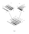
- Fig. 5 illustrates how such a three-dimensional electronic structure can be made.
- the second electrode module 20 is first folded over along the line L1, in such a way that the upper silicon layer (second substrate) 72 'faces outward and the lower silicon layer (first substrate) 71' is oriented inwardly, see.
- Fig. 5A When the line All passes in the middle of the electrode module 20, a folded half-size electrode module 20 is formed. Then, the resulting sides of the electrode module 20 are buckled along the lines L2 and L3, such that the resulting shape in profile represents an inverted T with two half-legs 22 and 23 and a vertical 21.
- the T-shaped profile must not be symmetrical, folds and kinks along other lines are conceivable, the proportions of the surfaces may be different than in Fig. 5 be illustrated.
- the three-dimensional structure is particularly suitable when signals of mutually opposite brain areas are to be detected and e.g. the space is insufficient for two separate structures.
- the electrode structure according to the design can then be produced by the method described above.
- the design can be tested computerized, e.g. Simulations can be performed.
Landscapes
- Health & Medical Sciences (AREA)
- Life Sciences & Earth Sciences (AREA)
- Animal Behavior & Ethology (AREA)
- Veterinary Medicine (AREA)
- Public Health (AREA)
- Engineering & Computer Science (AREA)
- Biomedical Technology (AREA)
- Heart & Thoracic Surgery (AREA)
- General Health & Medical Sciences (AREA)
- Neurology (AREA)
- Neurosurgery (AREA)
- Surgery (AREA)
- Molecular Biology (AREA)
- Medical Informatics (AREA)
- Pathology (AREA)
- Biophysics (AREA)
- Physics & Mathematics (AREA)
- Psychology (AREA)
- Cardiology (AREA)
- Nuclear Medicine, Radiotherapy & Molecular Imaging (AREA)
- Radiology & Medical Imaging (AREA)
- Electrotherapy Devices (AREA)
Abstract
Description
- Die Erfindung betrifft ein Verfahren zum Herstellen einer Elektrodenstruktur für eine neuronale Schnittstelle sowie eine Elektrodenstruktur für eine neuronale Schnittstelle, insbesondere zur Implantation in ein Gehirn.
- Neuronale Schnittstellen, welche in ein Gehirn implantiert werden können, weisen Elektroden auf, welche zur Ableitung von Neuronenaktivitäten, d.h. zum Messen von Gehirnströmen oder zur Stimulation bestimmter Hirnareale dienen. Hierfür werden etwa Elektrokortikogramm-Elektroden (ECoG-Elektroden) oder Cuff Elektroden verwendet.
- Die Implantation von ECoG-Elektroden in ein Gehirn ist beispielsweise bei der prächirurgischen Epilepsie-Diagnostik bekannt. ECoG-Elektroden werden auch bei der Resektion von Gehirntumoren eingesetzt, um durch Stimulation bestimmter Gehirnareale zu erkennen, ob es sich bei dem Gehirnareal um ein funktionell wichtiges Gehirnareal handelt, welches auf keinen Fall operativ entfernt werden sollte.
- Die mit Hilfe der ECoG-Elektroden gemessenen Gehirnströme können etwa einer Gehirn-Computer-Schnittstelle (Brain-Computer-Interface, BCI) zugeführt und dort ausgewertet werden. Mit dem Ergebnis der Auswertung kann beispielsweise eine Prothese gesteuert werden. Mit Hilfe solcher Gehim-Computer-Schnittstellen können etwa behinderte Menschen mittels ihrer Gedanken Prothesen oder dergleichen steuern.
- Mit Cuff-Elektroden können etwa periphere Nerven stimuliert und/oder deren Signale abgeleitet und einer Gehirn-Computer-Schnittstelle zugeführt werden. Cuff Elektroden werden auch in klinischen Anwendungen eingesetzt.
- Es ist bekannt, Elektroden für neuronale Schnittstellen sandwichartig zwischen zwei Trägermaterialien, etwa zwischen zwei Silikonfolien, einzubetten.
- Um eine möglichst präzise Aufzeichnung von Gehirnströmen bzw. eine möglichst präzise Stimulation bestimmter Hirnareale zu erreichen, ist es notwendig, Elektrodenstrukturen mit einer möglichst hohen Auflösung zu verwenden, wobei die Auflösung durch die Anzahl der Elektrodenkontaktflächen auf einer vorbestimmten Fläche definiert ist. Die Auflösung der Elektrodenstruktur kann dadurch erhöht werden, dass die Anzahl der zwischen den beiden Silikonfolien eingebetteten Elektroden bzw. Elektrodenkontaktflächen erhöht wird.
- Die maximale Anzahl von Elektrodenkontaktflächen und damit die maximale Auflösung der Elektrodenstruktur auf dem Trägermaterial sind allerdings begrenzt, weil auf der zur Verfügung stehenden Gesamtfläche des Trägermaterials neben den Elektrodenkontaktflächen auch noch die Leiterbahnen, welche die Elektrodenkontaktflächen mit Elektrodenanschlussflächen verbinden, untergebracht werden müssen. Das bedeutet, dass für eine hoch aufgelöste Elektrodenstruktur nur ein kleiner Teil der Gesamtfläche des Trägermaterials für die Anordnung der Elektrodenkontaktflächen zur Verfügung steht. Hierbei gilt, dass bei gleichbleibender Gesamtfläche des Trägermaterials die für die Anordnung der Elektrodenkontaktflächen zur Verfügung stehende Fläche mit zunehmender Auflösung kleiner wird, weil mit zunehmender Auflösung auch die Anzahl der Leiterbahnen zunimmt.
- Die Gesamtfläche des Trägermaterials kann allerdings nicht einfach vergrößert werden, weil bei einer Herstellung der Elektrodenkontaktflächen und Leiterbahnen mit einem Laser die im Bereich des Randes des Trägermaterials herzustellenden Elektrodenkontaktflächen und Leiterbahnen nicht mehr im Fokus des Lasers liegen. Die im Bereich des Randes des Trägermaterials herzustellenden Elektrodenkontaktflächen und Leiterbahnen können daher nicht mit derselben Genauigkeit hergestellt werden wie die im mittleren Bereich des Trägermaterials herzustellenden Elektrodenkontaktflächen und Leiterbahnen. Damit erhöht sich mit zunehmender Gesamtfläche des Trägermaterials auch die Wahrscheinlichkeit eines Fehlers während des Herstellungsprozesses, was einen größeren Ausschuss zur Folge hat.
- Um das Problem der maximal möglichen Auflösung bei gleichbleibender Gesamtfläche des Trägermaterials zu umgehen, ist es bekannt, mehrschichtige Elektrodenstrukturen zu verwenden, wobei in einer oberen Schicht die Elektrodenkontaktflächen und Leiterbahnen so angeordnet werden, dass sich unterhalb dieser Elektrodenkontaktflächen und Leiterbahnen keine Elektrodenkontaktflächen der darunterliegenden Schichten befinden.
- Um solche mehrschichtigen Elektrodenstrukturen herzustellen, ist es bekannt, diese schichtweise aufzubauen. Dabei wird zunächst auf einem ersten Trägermaterial eine Elektrodenstruktur mit Elektrodenkontaktflächen und Leiterbahnen erzeugt. Das Erzeugen der Elektrodenkontaktflächen und der Leiterbahnen kann beispielsweise mit Hilfe eines Lasers bewerkstelligt werden. In einem weiteren Schritt wird auf die so erzeugte Elektrodenstruktur ein weiteres Trägermaterial aufgetragen, auf welcher wiederum eine Elektrodenstruktur mit Elektrodenkontaktflächen und Leiterbahnen mit Hilfe eines Lasers erzeugt werden. Nach dem Erzeugen der zweiten Elektrodenstruktur wird eine weitere Trägerschicht aufgetragen. Die Schritte für das Erzeugen der zweiten Elektrodenstruktur und das Auftragen eines weiteren Trägermaterials können für weitere Elektrodenschichten wiederholt werden.
- Dieses Verfahren weist allerdings den gravierenden Nachteil auf, dass bei der Herstellung einer oberen Elektrodenstruktur mittels eines Lasers darunterliegende Elektrodenstrukturen beschädigt werden können. Um dies zu vermeiden, können einerseits die Abstände der einzelnen Elektrodenstrukturen so gewählt werden, dass ein Beschädigen einer darunterliegenden Elektrodenstruktur mit dem Laser sicher verhindert wird. Andererseits kann die Anordnung der Elektrodenkontaktflächen und der Leiterbahnflächen einer oberen Elektrodenstruktur so gewählt werden, dass sich ein möglichst kleiner Anteil der darunterliegenden Elektrodenstruktur im Bearbeitungsbereich des Lasers zur Herstellung der oberen Elektrodenstruktur befindet.
- Im ersteren Fall hat ein Vergrößern des Abstandes der einzelnen Elektrodenschichten allerdings den Nachteil, dass sich damit auch die Dicke der gesamten Elektrode vergrößert, was sich etwa bei der Implantation nachteilig auswirkt. Im letzteren Fall könnte nicht die gesamte Fläche zur Herstellung von Elektrodenkontaktflächen verwendet werden, so dass keine optimale Ausnutzung der Gesamtfläche des Trägermaterials erreicht wird. Zudem kann ein Beschädigen darunterliegender Elektrodenstrukturen damit nicht ausgeschlossen werden.
- Aufgabe der vorliegenden Erfindung ist es daher, ein Herstellungsverfahren für eine Elektrodenstruktur insbesondere für eine neuronale Schnittstelle anzugeben, welches die Herstellung besonders hoch auflösender Elektrodenstrukturen ermöglicht, ohne dabei die aus dem Stand der Technik bekannten Nachteile aufzuweisen. Des Weiteren ist es Aufgabe, eine derartige Elektrodenstruktur bereitzustellen.
- Diese Aufgabe wird durch ein Verfahren zum Herstellen einer Elektrodenstruktur für neuronale Schnittstellen sowie durch eine Elektrodenstruktur für eine neuronale Schnittstelle nach den unabhängigen Ansprüchen gelöst. Vorteilhafte Ausgestaltungen und Weiterbildungen der Erfindung sind in den jeweiligen abhängigen Ansprüchen angegeben.
- Erfindungsgemäß bereitgestellt wird also ein Verfahren zum Herstellen einer Elektrodenstruktur insbesondere für eine neuronale Schnittstelle, wobei das Verfahren das Herstellen eines ersten Elektrodenmoduls und wenigstens eines zweiten Elektrodenmoduls umfasst, wobei jeweils
- auf einem ersten Substrat eine Anzahl von Elektrodenkontaktflächen und eine Anzahl von Leiterbahnen erzeugt werden,
- auf dem ersten Substrat und den darauf erzeugten Elektrodenkontaktflächen und Leiterbahnen ein zweites Substrat aufgebracht wird, und
- in dem jeweiligen zweiten Substrat im Bereich der Elektrodenkontaktflächen Öffnungen hergestellt werden, und
- Die einzelnen Elektrodenmodule, die jeweils ein erstes Substrat, Elektrodenkontaktflächen und Leiterbahnen sowie darüber ein zweites Substrat umfassen, werden also getrennt voneinander hergestellt und erst danach zu der Elektrodenstruktur zusammengefügt. Dieses Verfahren hat zunächst den Vorteil, dass z.B. bei einem Produktionsfehler bei der Herstellung eines der Elektrodenmodule nur dieses eine Elektrodenmodul unbrauchbar wird, nicht aber die übrigen. Die einzelnen Elektrodenmodule können also unmittelbar nach ihrer Herstellung auf Fehler überprüft werden und dann aussortiert werden, bevor sie zur Elektrodenstruktur zusammengefügt werden. Die Modularisierung der Herstellung bringt weitere Vorteile mit sich. So wird die Herstellung der Elektrodenstruktur vereinfacht. Zudem können hoch auflösende Elektrodenmodule hergestellt werden, welche zusammen eine besonders hoch auflösende Elektrodenstruktur bilden. Aufgrund der Modularisierung könnten häufiger benötigte Teile könnten vorentworfen und gefertigt werden und so in einem Baukastensystem zu Bildung von komplexere Elektrodenstrukturen bereitgehalten werden.
- Es entsteht eine sehr flexible Elektrodenstruktur, die sich hervorragend zur Bildung von flächenförmigen Sensoren eignet, die z.B. in ein Gehirn implantierbar sind.
- Die Elektrodenkontaktflächen und die Leiterbahnen des wenigstens einen zweiten Elektrodenmoduls werden bevorzugt so erzeugt, dass sie beim Aufbringen des zweiten Elektrodenmoduls auf das erste Elektrodenmodul die Elektrodenkontaktflächen des ersten Elektrodenmoduls nicht abdecken.
- Die Elektrodenkontaktflächen des ersten Elektrodenmoduls und des wenigstens einen zweiten Elektrodenmoduls bilden zusammen die Elektrodenkontaktflächen der Elektrodenstruktur. Dadurch kann in vorteilhafter Weise die Gesamtfläche der Elektrodenstruktur für die Anordnung von Elektrodenkontaktflächen ausgenutzt werden.
- Die Elektrodenauflösung des ersten Elektrodenmoduls kann verschieden von der Elektrodenauflösung des wenigstens einen zweiten Elektrodenmoduls sein, wobei die Elektrodenauflösung als die Anzahl der Elektrodenkontaktflächen pro Flächeneinheit definiert ist.
- Dadurch wird es möglich, eine Elektrodenstruktur mit lokal unterschiedlichen Auflösungen bereitzustellen. So muss, wenn z.B. auf einem Teil der Oberfläche der Elektrodenstruktur eine sehr viel höhere Auflösung (oder Anzahl von Elektrodenkontaktflächen) gefordert wird als auf einem anderen, nur dieser Teil durch ein Elektrodenmodul gebildet werden, das mit einer höheren Präzision gefertigt wird als der andere Teil. Diese Aufteilung bringt erhebliche Vorteile in den Produktionskosten mit sich, denn mit der geforderten Präzision (oder Auflösung) steigen der Herstellungsaufwand und die Ausschussrate.
- Es hat sich als vorteilhaft herausgestellt, vor dem Aufbringen des wenigstens einen zweiten Elektrodenmoduls auf das erste Elektrodenmodul auf dem zweiten Substrat des ersten Elektrodenmoduls ein Lösungsmittel aufzubringen.
- Dadurch kann das wenigstens eine zweite Elektrodenmodul exakt auf dem ersten Elektrodenmodul ausgerichtet werden.
- In wenigstens einem der Elektrodenmodule können Kanäle erzeugt werden, welche jeweils eine Eintrittsöffnung und wenigstens eine Austrittsöffnung aufweisen, zum Transport eines Fluid. Derartige mikrofluidische Kanäle können zur gezielten Medikamentenabgabe vorgesehen sein.
- Das erste Substrat und/oder das zweite Substrat werden vorzugsweise aus der Gruppe der synthetischen Polymere, besonders bevorzugt aus der Gruppe der Poly(organo)siloxane ausgewählt.
- Das erste Elektrodenmodul und das wenigstens eine zweite Elektrodenmodul können rechnergestützt entworfen werden.
- Die auf dem ersten Substrat zu erzeugenden Elektrodenkontaktflächen und Leiterbahnen können im Laserschneidverfahren auf dem ersten Substrat erzeugt werden. Die mikrofluidischen Kanäle können ebenfalls im Laserschneidverfahren hergestellt werden.
- In wenigstens einem der Elektrodenmodule kann wenigstens ein Lichtwellenleiter integriert werden, welcher an dem zweiten Substrat nach außen geführt wird.
- Bereitgestellt wird auch eine Elektrodenstruktur insbesondere für eine neuronale Schnittstelle, umfassend ein erstes Elektrodenmodul und wenigstens ein zweites Elektrodenmodul, welche jeweils ein erstes Substrat, auf welchem eine Anzahl von Elektrodenkontaktflächen und eine Anzahl von Leiterbahnen angeordnet sind, und ein zweites Substrat, welches auf dem ersten Substrat und den darauf angeordneten Elektrodenkontaktflächen und Leiterbahnen angeordnet ist, auf weisen, wobei das wenigstens eine zweite Elektrodenmodul auf dem ersten Elektrodenmodul angeordnet ist, wobei in dem wenigstens einen zweiten Elektrodenmodul (20) Löcher (60) angeordnet sind, welche jeweils das erste Substrat (71') und das zweite Substrat (72') des zweiten Elektrodenmoduls (20) durchdringen, wobei die Löcher (60) so angeordnet sind, dass sie jeweils mit wenigstens einer Elektrodenkontaktfläche (50) des ersten Elektrodenmoduls (10) korrespondieren.
- Die Elektrodenkontaktflächen und die Leiterbahnen des wenigstens einen zweiten Elektrodenmoduls können so angeordnet sein, dass sie die Elektrodenkontaktflächen des ersten Elektrodenmoduls nicht abdecken.
- Die Elektrodenauflösung des ersten Elektrodenmoduls kann verschieden von der Elektrodenauflösung des wenigstens einen zweiten Elektrodenmoduls sein, wobei die Elektrodenauflösung als die Anzahl der Elektrodenkontaktflächen pro Flächeneinheit definiert ist.
- Es sei darauf hingewiesen, dass die einzelnen Elektrodenmodule in ihrer Größe, d.h. Oberfläche, nicht deckungsgleich sein müssen. Elektrodenmodule können auch nebeneinander auf ein darunterliegendes Elektrodenmodul gesetzt werden.
- Weitere Einzelheiten und Merkmale der Erfindung sowie konkrete Ausführungsbeispiele der Erfindung ergeben sich aus der nachfolgenden Beschreibung in Verbindung mit der Zeichnung. Es zeigt:
- Fig. 1
- einen Ausschnitt eines ersten Elektrodenmoduls und eines zweiten Elektrodenmoduls einer erfindungsgemäßen Elektrodenstruktur im Querschnitt;
- Fig. 2
- einen Ausschnitt von zwei Elektrodenmodulen einer erfindungsgemäβen Elektrodenstruktur im zusammengesetzten Zustand im Querschnitt;
- Fig. 3
- ein konkretes Ausführungsbeispiel von zwei Elektrodenmodulen, welche zu einer erfindungsgemäßen Elektrodenstruktur zusammengesetzt werden, wobei die beiden Elektrodenmodule jeweils die gleiche Auflösung aufweisen;
- Fig. 4
- zwei Elektrodenmodule, welche zu einer erfindungsgemäßen Elektrodenstruktur zusammengesetzt werden, wobei die beiden Elektrodenmodule jeweils eine unterschiedliche Auflösung aufweisen; und
- Fig. 5
- ein weiteres Ausführungsbeispiel der vorliegenden Erfindung.
-
Fig. 1 zeigt ein erstes Elektrodenmodul 10 und ein zweites Elektrodenmodul 20, welche jeweils getrennt voneinander hergestellt werden und nach der Herstellung erfindungsgemäß zusammengesetzt werden, um dann die endgültige Elektrodenstruktur zu bilden. - Es wird zunächst angegeben, wie die einzelnen Elektrodenmodule 10, 20 hergestellt werden, bevor mit Bezug auf
Fig. 2 angegeben wird, wie aus den einzelnen Elektrodenmodulen eine endgültige Elektrodenstruktur gemäß der Erfindung hergestellt wird. - Zur Herstellung des ersten Elektrodenmoduls wird zunächst auf einem Objektträger, etwa eine Glasscheibe, ein Klebeband aufgewalzt. Das Klebeband ist dazu vorgesehen, damit das erste Elektrodenmodul 10 am Ende des Herstellungsprozesses leicht von diesem abgelöst werden kann. Anstelle eines Klebebandes kann auch eine Folie aus ausgehärtetem Silikon verwendet werden.
- Auf das Klebeband wird ein erstes Substrat 71, welches hier mit Heptan, vorzugsweise mit n-Heptan verdünntes Silikon ist, aufgeschleudert. Diese Silikonschicht bildet die untere Silikonschicht 71, auf welcher die Elektrodenkontaktflächen und die Leiterbahnen der Elektrodenstruktur des ersten Elektrodenmoduls 10 erzeugt werden. Die untere Silikonschicht 71 des ersten Elektrodenmoduls 10 wird an der Anschlussseite mit einem Laser strukturiert, um im weiteren Herstellungsverfahren Metallstrukturen zu erhalten, an welche beispielsweise Verbindungskabel angebracht werden können.
- Nachdem die aufgeschleuderte untere Silikonschicht 71 hinreichend weit ausgehärtet ist, wird auf die untere Silikonschicht 71 eine Metallfolie aufgewalzt. Die Metallfolie kann etwa Platin, Edelstahl oder eine Legierung auf Nickel-Kobalt-Basis (z.B. MP35N-Legierung) aufweisen. Die Dicke der Metallfolie kann zwischen etwa 5 11m und 50 µm betragen.
- In einem weiteren Schritt wird die aufgewalzte Metallfolie mit einem Laser strukturiert, um Elektrodenkontaktflächen 50 und Leiterbahnen 30 zu bilden. Herausgetrennte Metallreste werden von der unteren Silikonschicht 71 entfernt. Dies kann manuell mit Hilfe einer Pinzette erfolgen. Das Entfernen der Metallreste kann aber auch maschinell erfolgen.
- Sobald die erforderliche Elektrodenstruktur, d.h. die Elektrodenkontaktflächen 50 und die Leiterbahnen 30, auf der unteren Silikonschicht 71 fertig hergestellt sind, wird auf die untere Silikonschicht 71 und auf die auf der unteren Silikonschicht 71 erzeugte Elektrodenstruktur ein zweites Substrat, vorzugsweise eine zweite Silikonschicht 72, aufgeschleudert. Die zweite Silikonschicht 72 wird vorzugsweise ebenfalls mit n-Heptan verdünnt.
- Nach dem Aushärten der zweiten Silikonschicht 72 werden Öffnungen erzeugt, um die Elektrodenkontaktflächen freizulegen, so dass bei einem späteren Gebrauch der erfindungsgemäßen Elektrodenstruktur ein Kontakt zwischen einem Gewebe und der Elektrodenkontaktfläche hergestellt werden kann. Das Erzeugen dieser Öffnungen wird hier ebenfalls mit Hilfe des Lasers bewerkstelligt. Die Oberseite der an der Anschlussseite verlaufenden Metallstrukturen, an welchen etwa ein Kabel angeschlossen werden kann, kann ebenfalls mit Hilfe des Lasers freigelegt werden.
- Alternativ können die Metallstrukturen an der Anschlussseite auch mit Hilfe einer Polyamidfolie (z.B. Kaptonfolie) freigelegt werden, indem vor dem Auf bringen der oberen Silikonschicht 72 eine strukturierte Maske aus Polyamid an der Anschlussseite auf die Metallstrukturen aufgebracht wird. Die Polyamidfolie kann ebenfalls mit Hilfe eines Lasers strukturiert werden. Nach dem Aufbringen der oberen Silikonschicht 72 kann die strukturierte Polyamidfolie zusammen mit dem auf ihr aufgebrachten Silikon entfernt werden.
- In einem abschließenden Schritt kann mit dem Laser noch eine Umrandung erzeugt werden, indem mit dem Laser ein umlaufender Schnitt erzeugt wird, welcher sowohl die obere Silikonschicht 72 als auch die untere Silikonschicht 71 durchschneidet.
- Das so erzeugte erste Elektrodenmodul 10 kann nun von dem Klebeband abgelöst werden. Das erste Elektrodenmodul 10 weist nun eine Anzahl von Elektrodenkontaktflächen 50 und eine Anzahl von Leiterbahnen 30 auf, wobei die obere Silikonschicht 72 im Bereich der Elektrodenkontaktflächen 50 Öffnungen auf weist, so dass die Elektrodenkontaktflächen 50 freigelegt sind. Die Dicke des ersten Elektrodenmoduls 10 beträgt zwischen 50 11m und 150 11m.
- Das zweite Elektrodenmodul 20 wird im Wesentlichen mit demselben Verfahren hergestellt wie das erste Elektrodenmodul 10. Die Elektrodenkontaktflächen 50' und die Leiterbahnen 30' des zweiten Elektrodenmoduls 20 werden so angeordnet, dass sie die Elektrodenkontaktflächen 50 des ersten Elektrodenmoduls 10 nicht abdecken, wenn das zweite Elektrodenmodul 20 auf dem ersten Elektrodenmodul 10 aufgebracht wird, wie mit Bezug auf
Fig. 2 näher beschrieben wird. - Die Elektrodenkontaktflächen 50' bzw. die Leiterbahnen 30' des zweiten Elektrodenmoduls 20 können aber so angeordnet werden, dass sie nach dem Aufbringen des zweiten Elektrodenmoduls 20 auf das erste Elektrodenmodul 10 die Leiterbahnen 30 des ersten Elektrodenmoduls 10 teilweise oder vollständig abdecken. Dadurch wird in vorteilhafter Weise erreicht, dass im Gegensatz zu einschichtigen Elektrodenstrukturen nahezu die gesamte Fläche des Elektrodenträgers zur Anordnung von Elektrodenkontaktflächen 50, 50' zur Verfügung steht, weil auf dem zweiten Elektrodenmodul 20 die Elektrodenkontaktflächen 50' auch dort angeordnet werden können, wo bei dem ersten Elektrodenmodul die Leiterbahnen 30 verlaufen.
- Zusätzlich werden in dem zweiten Elektrodenmodul 20 Löcher 60 erzeugt, welche das zweite Elektrodenmodul 20 vollständig durchdringen. Die Löcher 60 werden so an dem zweiten Elektrodenmodul 20 angeordnet, dass sie nach dem Aufbringen des zweiten Elektrodenmoduls 20 auf das erste Elektrodenmodul 10 mit den Elektrodenkontaktflächen 50 des ersten Elektrodenmoduls 10 korrespondieren. Damit wird sichergestellt, dass nach dem Aufbringen des zweiten Elektrodenmoduls 20 auf das erste Elektrodenmodul 10 die Elektrodenkontaktflächen 50 des ersten Elektrodenmoduls 10 weiterhin frei liegen. Die Dicke des zweiten Elektrodenmoduls 20 beträgt zwischen 50 µm und 150 11m.
- Die Löcher 60 können mit Hilfe des Lasers erzeugt werden. Alternativ können die Löcher 60 auch in einem Stanzverfahren hergestellt werden.
- Das getrennte Herstellen der beiden Elektrodenmodule 10, 20 hat den wesentlichen Vorteil, dass beide Elektrodenmodule im Wesentlichen mit dem gleichen Herstellungsverfahren hergestellt werden können, ohne dass dabei darunterliegende Elektrodenstrukturen, etwa des ersten Elektrodenmoduls 10, beschädigt werden.
- Die Anordnung der Elektrodenkontaktflächen 50, 50', der Leiterbahnen 30, 30' sowie der Elektrodenanschlussflächen 40, 40' der beiden Elektrodenmodule 10, 20 kann etwa mit Hilfe einer CAD-Software geplant und getestet werden. Durch die Verwendung eines Lasers zum Erzeugen der Elektrodenstrukturen auf dem ersten und dem zweiten Elektrodenmodul können zum Einen Objektgrößen von bis herunter zu 50 µm erzeugt werden, und zum Anderen können die Elektrodenkontaktflächen bzw. die Leiterbahnen so exakt erzeugt werden, dass eine Anordnung des zweiten Elektrodenmoduls 20 auf das erste Elektrodenmodul 10 wie geplant erfolgen kann.
-
Fig. 2 zeigt eine erfindungsgemäße Elektrodenstruktur mit einem ersten Elektrodenmodul 10 und einem zweiten Elektrodenmodul 20, welche miteinander verbunden sind. Die beiden Elektrodenmodule 10, 20 werden wie mit Bezug aufFig. 1 beschrieben hergestellt. Vor dem Zusammenfügen der beiden Elektrodenmodule 10, 20 bzw. vor dem Anordnen des zweiten Elektrodenmoduls 20 auf dem ersten Elektrodenmodul 10 wird an der oberen Silikonschicht 72 des ersten Elektrodenmoduls 10 ein Lösungsmittel aufgebracht, welches eine genaue Justierung des zweiten Elektrodenmoduls 20 auf dem ersten Elektrodenmodul 10 ermöglicht. Als Lösungsmittel kann etwa Methanol verwendet werden. Methanol als Lösungsmittel hat den Vorteil, dass die obere Silikonschicht 72 des ersten Elektrodenmoduls 10 und die untere Silikonschicht 71' des zweiten Elektrodenmoduls 20 nur sehr gering aufquellen. - Nach dem Aufbringen des zweiten Elektrodenmoduls 20 auf das erste Elektrodenmodul 10 werden die Elektrodenmodule 10, 20 unlösbar miteinander verbunden. Das kann beispielsweise im Plasmabond-Verfahren erfolgen.
- Dabei wird die Unterseite des zweiten Elektrodenmoduls 20 im Sauerstoffplasma aktiviert, wobei die Unterseite reaktiv wird. Das zweite Elektrodenmodul 20 wird dann auf das mit dem Lösungsmittel versehene erste Elektrodenmodul 10 aufgebracht. Das Lösungsmittel erlaubt ein genaues Ausrichten des zweiten Elektrodenmoduls 20 auf dem ersten Elektrodenmodul 10. Das Lösungsmittel verhindert zudem, dass sich zwischen den Elektrodenmodulen Luftblasen bilden. Sobald das Lösungsmittel verdampft ist, sind die Elektrodenmodule 10, 20 unlösbar miteinander verbunden. Das Verdampfen des Lösungsmittels benötigt etwa 10 Minuten. Während dieser Zeit kann das zweite Elektrodenmodul 20 auf dem ersten Elektrodenmodul 10 justiert werden.
- Das unlösbare Verbinden der beiden Elektrodenmodule 10, 20 kann auch mit anderen geeigneten Verfahren bzw. Mitteln durchgeführt werden.
- Wie aus
Fig. 2 ersichtlich, können die Elektrodenkontaktflächen 50 und 50' des ersten Elektrodenmoduls 10 bzw. des zweiten Elektrodenmoduls 20 eine unterschiedliche Fläche aufweisen, d.h. sie können unterschiedlich groß sein. Auch können die einzelnen Elektrodenkontaktflächen eines Elektrodenmoduls eine unterschiedliche Fläche aufweisen. Damit kann eine Elektrodenstruktur mit unterschiedlichen Auflösungen hergestellt werden, wie mit Bezug auf dieFig. 3 und4 näher beschrieben wird. - Auf dem ersten Elektrodenmodul 10 können auch mehrere zweite Elektrodenmodule 20 nebeneinander angeordnet werden. Die nebeneinander angeordneten Elektrodenmodule 20 können dabei jeweils eine verschiedene Auflösung aufweisen. Dies hat den Vorteil, dass die zweiten Elektrodenmodule 20 jeweils mit einer Auflösung hergestellt werden können und anschließend zu einer zweiten Elektrodenschicht mit unterschiedlichen Auflösungen zusammen gesetzt werden können.
-
Fig. 3 zeigt eine erfindungsgemäße Elektrodenstruktur, welche durch Zusammensetzen eines ersten Elektrodenmoduls 10 und eines zweiten Elektrodenmoduls 20 hergestellt wird. Die Elektrodenmodule 10, 20 weisen hierbei jeweils die gleiche Auflösung auf. - Das erste Elektrodenmodul 10 weist eine Anzahl von Elektrodenkontaktflächen 50 auf, welche jeweils über eine Leiterbahn 30 mit Elektrodenanschlussflächen 40 verbunden sind.
- Das zweite Elektrodenmodul 20 weist ebenfalls eine Anzahl von Elektrodenkontaktflächen 50' auf, welche über Leiterbahnen 30' mit einer Anzahl von Elektrodenanschlussflächen 40' verbunden sind.
- Die Anordnung der Elektrodenkontaktflächen 50' auf dem zweiten Elektrodenmodul 20 ist hier so gewählt, dass diese nach dem Zusammenfügen bzw. nach dem Anordnen des zweiten Elektrodenmoduls 20 auf dem ersten Elektrodenmodul 10 sich im Wesentlichen im Bereich der Leiterbahnen 30 des ersten Elektrodenmoduls 10 befinden. Wie aus
Fig. 3 besonders gut erkennbar ist, kann die Auflösung der Elektrodenstruktur durch Aufbringen des zweiten Elektrodenmoduls 20 auf das erste Elektrodenmodul 10 verdoppelt werden. -
Fig. 4 zeigt ein weiteres konkretes Beispiel einer erfindungsgemäßen Elektrodenstruktur, bei welchem ein erstes Elektrodenmodul 10 und ein zweites Elektrodenmodul 20 zusammengefügt werden. In dem inFig. 4 gezeigtem Beispiel ist die Auflösung des ersten Elektrodenmoduls 10 verschieden von der Auflösung des zweiten Elektrodenmoduls 10. An dem ersten Elektrodenmodul 10 sind eine Anzahl von Elektrodenkontaktflächen 50 angeordnet, welche jeweils über eine Leiterbahn 30 mit Elektrodenanschlussflächen 40 verbunden sind. An dem zweiten Elektrodenmodul 20 sind eine Anzahl von Elektrodenkontaktflächen 50' angeordnet, welche ebenfalls über Leiterbahnen 30' mit Elektrodenanschlussflächen 40' verbunden sind. Die Elektrodenkontaktflächen 50' des zweiten Elektrodenmoduls 20 sind hier kleiner gewählt als die Elektrodenkontaktflächen 50 des ersten Elektrodenmoduls 10. - Zusätzlich sind in dem zweiten Elektrodenmodul 20 Löcher 60 vorgesehen, welche so angeordnet sind, dass sie im Wesentlichen mit den Elektrodenkontaktflächen 50 des ersten Elektrodenmoduls korrespondieren, so dass eine Kontaktierung der Elektrodenkontaktflächen 50 des ersten Elektrodenmoduls mit einem Gewebe auch nach dem Aufbringen des zweiten Elektrodenmoduls 20 auf das erste Elektrodenmodul 10 gewährleistet ist.
- Zusätzlich oder alternativ zu den Elektrodenkontaktflächen 50, 50' bzw. Leiterbahnen 30, 30' können in einem der Elektrodenmodule 10, 20 auch Kanäle vorgesehen sein, welche beispielsweise im Anschlussbereich eine Eintrittsöffnung und an der oberen Silikonschicht 72 bzw. 72' eine Austrittsöffnung aufweisen. Derartige mikrofluidische Kanäle können etwa dazu vorgesehen sein, um eine zielgerichtete Medikamentenabgabe durchzuführen. So kann beispielsweise ein Elektroden-Implantat mit zwei Modulen hergestellt werden, wobei ein erstes Modul als Elektrodenmodul ausgestaltet ist und ein zweites Modul zusätzlich oder alternativ zu den Elektrodenkontaktflächen eine Anzahl von mikrofluidischen Kanälen, etwa zur Medikamentenabgabe, aufweist.
- Die für die Erzeugung derartiger mikrofluidischer Kanäle erforderlichen Verfahrensschritte können in das mit Bezug auf
Fig. 1 erläuterte Verfahren integriert werden. - Alternativ können die mikrofluidischen Kanäle auch zwischen zwei Elektrodenmodulen erzeugt werden. So können beispielsweise nach dem Aufbringen der oberen Silikonschicht 72 des ersten Elektrodenmoduls 10 mit Hilfe des Lasers in der oberen Silikonschicht 72 die entsprechenden Kanäle erzeugt werden. In dem zweiten Elektrodenmodul 20 können ebenfalls mit Hilfe des Lasers entsprechende Austrittsöffnungen hergestellt werden, welche mit den Kanälen auf dem ersten Elektrodenmodul korrespondieren. Nach dem Aufbringen des zweiten Elektrodenmoduls 20 auf das erste Elektrodenmodul 10 werden dann im Wesentlichen geschlossene mikrofluidische Kanäle mit Eintritts- und Austrittsöff nungen gebildet.
- Zusätzlich oder alternativ zu den mikrofluidischen Kanälen können auch optische Module in die Elektrodenmodule 10 bzw. 20 integriert werden. Beispielsweise können in das Elektrodenmodul 20 Lichtwellenleiter integriert werden, welche an der oberen Silikonschicht 72' sowie an der Anschlussseite des Elektrodenmoduls 20 nach außen geführt werden. Mit Hilfe der integrierten Lichtwellenleiter können bestimmte Gehirnregionen zusätzlich stimuliert werden.
- Die Erfindung lässt sich zur Bildung einer dreidimensionalen Elektrodenstruktur erweitern.
Fig. 5 illustriert, wie eine derartige dreidimensionale Elektronenstruktur hergestellt werden kann. Vor dem Aufbringen eines zweiten Elektrodenmoduls 20 auf das erste Elektrodenmodul 10 wird das zweite Elektrodenmodul 20 zunächst entlang der Linie L1 umgefaltet, und zwar so, dass die obere Silikonschicht (zweites Substrat) 72' nach außen zeigt und die untere Silikonschicht (erstes Substrat) 71' nach innen orientiert ist, vgl.Fig. 5A . Wenn die Linie All in der Mitte des Elektrodenmoduls 20 verläuft, entsteht ein gefaltetes Elektrodenmodul 20 halber Größe. Sodann werden die so entstehenden Seiten des Elektrodenmoduls 20 entlang der Linien L2 und L3 aufgeknickt, derart, dass die resultierende Form im Profil ein umgekehrtes T mit zwei Halbschenkeln 22 und 23 und einer Senkrechten 21 darstellt. Schließlich wird das gefaltete und geknickte zweite Elektrodenmodul 20 (als umgekehrtes T, also "kopfüber") auf das erste Elektrodenmodul 10 (Fig. 5B ) aufgebracht, wie zuvor beschrieben. Es entsteht eine dreidimensionale Trägerstruktur, wie sie inFig. 5C dargestellt ist. - Selbstverständlich muss das T-förmige Profil nicht symmetrisch sein, Faltungen und Knickungen entlang anderer Linien sind denkbar, die Proportionen der Flächen können anders als in
Fig. 5 illustriert sein. - Die dreidimensionale Struktur eignet sich in besonderer Weise dann, wenn Signale einander gegenüber liegender Hirnareale erfasst werden sollen und z.B. der Raum für zwei separate Strukturen nicht ausreicht.
- Die Erfindung umfasst auch den rechnergestützten Entwurf einer Elektrodenstruktur insbesondere für eine neuronale Schnittstelle, wobei das Verfahren das Entwerfen eines ersten Elektrodenmoduls und wenigstens eines zweiten Elektrodenmoduls umfasst, wobei jeweils
- auf einem ersten Substrat eine Anzahl von Elektrodenkontaktflächen und eine Anzahl von Leiterbahnen erzeugt werden,
- auf dem ersten Substrat und den darauf erzeugten Elektrodenkontaktflächen und Leiterbahnen ein zweites Substrat aufgebracht wird, und
- in dem jeweiligen zweiten Substrat im Bereich der Elektrodenkontaktflächen Öffnungen hergestellt werden, und
- Die Elektrodenstruktur gemäß dem Entwurf kann dann mittels des oben beschriebenen Verfahrens hergestellt werden. Zuvor kann der Entwurf rechnergestützt getestet werden, z.B. können Simulationen durchgeführt werden.
- Alle vorteilhaften Weiterbildungen beziehen sich auch auf den rechnergestützten Entwurf.
-
- 10
- erstes Elektrodenmodul (erste Elektrodenschicht)
- 20
- zweites Elektrodenmodul (zweite Elektrodenschicht)
- 21
- Senkrechte
- 22
- Halbschenkel(-fläche)
- 23
- Halbschenkel(-fläche)
- 30, 30'
- Leiterbahnen
- 40, 40'
- Elektrodenanschlussflächen
- 50, 50'
- (geöffnete) Elektrodenkontaktflächen
- 60
- Löcher
- 71, 71'
- untere Silikonschicht (erstes Substrat)
- 72, 72'
- obere Silikonschicht (zweites Substrat)
- L1
- Faltungslinie
- L2
- Knicklinie
- L3
- Knicklinie
Claims (15)
- Verfahren zum Herstellen einer Elektrodenstruktur für eine neuronale Schnittstelle, wobei das Verfahren umfasst:- Herstellen eines ersten Elektrodenmoduls (10) und wenigstens eines zweiten Elektrodenmoduls (20), wobei für das erste Elektrodenmoduls (10) und für wenigstens ein zweites Elektrodenmoduls (20) jeweils- auf einem ersten Substrat (71, 71') eine Anzahl von Elektrodenkontaktflächen (50, 50') und eine Anzahl von Leiterbahnen (30, 30') erzeugt werden,- auf dem ersten Substrat (71, 71') und den darauf erzeugten Elektrodenkontaktflächen (50, 50') und Leiterbahnen (30, 30') ein zweites Substrat (72, 72') aufgebracht wird, und- in dem jeweiligen zweiten Substrat (72, 72') im Bereich der Elektrodenkontaktflächen (50, 50') Öffnungen hergestellt werden, und- Aufbringen des wenigstens einen zweiten Elektrodenmoduls (20) auf das erste Elektrodenmodul (10), wobei das erste Substrat (71') des wenigstens einen zweiten Elektrodenmoduls (20) auf dem zweiten Substrat (72) des ersten Elektrodenmoduls (10) angeordnet wird,wobei in dem wenigstens einen zweiten Elektrodenmodul (20) Löcher (60) erzeugt werden, welche jeweils das erste Substrat (71') und das zweite Substrat (72') des zweiten Elektrodenmoduls (20) durchdringen, wobei die Löcher (60) so angeordnet werden, dass sie beim Aufbringen des zweiten Elektrodenmoduls (20) auf das erste Elektrodenmodul (10) jeweils mit wenigstens einer Elektrodenkontaktfläche (50) des ersten Elektrodenmoduls (10) korrespondieren.
- Verfahren nach Anspruch 1, wobei die Elektrodenkontaktflächen (50') und die Leiterbahnen (30') des wenigstens einen zweiten Elektrodenmoduls (20) so erzeugt werden, dass sie beim Aufbringen des zweiten Elektrodenmoduls (20) auf das erste Elektrodenmodul (10) die Elektrodenkontaktflächen (50) des ersten Elektrodenmoduls (10) nicht abdecken.
- Verfahren nach einem der vorhergehenden Ansprüche, wobei die Elektrodenauflösung des ersten Elektrodenmoduls (10) verschieden von der Elektrodenauflösung wenigstens eines zweiten Elektrodenmoduls (20) gewählt wird, wobei die Elektrodenauflösung als die Anzahl der Elektrodenkontaktflächen pro Flächeneinheit definiert ist.
- Verfahren nach einem der vorhergehenden Ansprüche, wobei vor dem Aufbringen des wenigstens einen zweiten Elektrodenmoduls (20) auf das erste Elektrodenmodul (10) auf dem zweiten Substrat (72) des ersten Elektrodenmoduls (10) ein Lösungsmittel aufgebracht wird.
- Verfahren nach einem der vorhergehenden Ansprüche, wobei in wenigstens einem der Elektrodenmodule (10, 20) Kanäle erzeugt werden, welche jeweils eine Eintrittsöffnung und wenigstens eine Austrittsöffnung aufweisen, zum Transport eines Fluid.
- Verfahren nach einem der vorhergehenden Ansprüche, wobei das erste Substrat (71, 71') und/oder das zweite Substrat (72, 72') aus der Gruppe der synthetischen Polymere, vorzugsweise aus der Gruppe der Poly(organo)siloxane ausgewählt wird.
- Verfahren nach einem der vorhergehenden Ansprüche, wobei das erste Elektrodenmodul (10) und/oder das wenigstens eine zweite Elektrodenmodul (20) rechnergestützt entworfen werden.
- Verfahren nach einem der vorhergehenden Ansprüche, wobei die auf dem ersten Substrat (71, 71') zu erzeugenden Elektrodenkontaktflächen (50, 50') und Leiterbahnen (30, 30') im Laserschneidverfahren auf dem ersten Substrat (71, 71') erzeugt werden.
- Verfahren nach einem der vorhergehenden Ansprüche, wobei in wenigstens einem der Elektrodenmodule (10, 20) wenigstens ein Lichtwellenleiter integriert wird, welcher an dem zweiten Substrat (72, 72') nach außen geführt wird.
- Verfahren nach einem der vorhergehenden Ansprüche, wobei vor dem Aufbringen des wenigstens einen zweiten Elektrodenmoduls (20) auf das erste Elektrodenmodul (10) wenigstens ein zweites Elektrodenmodul (20) wenigstens einmal entlang einer Linie (L1) gefaltet wird.
- Verfahren nach Anspruch 10, wobei vor dem Aufbringen des wenigstens einen zweiten Elektrodenmoduls (20) auf das erste Elektrodenmodul (10) wenigstens ein zweites Elektrodenmodul (20) einmal entlang einer ersten Linie (L1) gefaltet wird, derart, dass das zweite Substrat (72') nach außen zeigt, und das wenigstens eine gefaltete zweite Elektrodenmodul (20) entlang einer zweiten Linie (L2) und entlang einer dritten Linie (L3) geknickt wird, derart, dass das resultierende wenigstens eine zweite Elektrodenmodul (20) im Profil ein umgekehrtes T-Profil darstellt.
- Elektrodenstruktur insbesondere für eine neuronale Schnittstelle, umfassend ein erstes Elektrodenmodul (10) und wenigstens ein zweites Elektrodenmodul (20), welche jeweils ein erstes Substrat (71, 71'), auf welchem eine Anzahl von Elektrodenkontaktflächen (50, 50') und eine Anzahl von Leiterbahnen (30, 30') angeordnet sind, und ein zweites Substrat (72, 72'), welches auf dem ersten Substrat (71, 71') und den darauf angeordneten Elektrodenkontaktflächen (50, 50') und Leiterbahnen (30, 30') angeordnet ist, aufweisen, wobei das wenigstens eine zweite Elektrodenmodul (20) auf dem ersten Elektrodenmodul (10) angeordnet ist,
wobei in dem wenigstens einen zweiten Elektrodenmodul (20) Löcher (60) angeordnet sind, welche jeweils das erste Substrat (71') und das zweite Substrat (72') des zweiten Elektrodenmoduls (20) durchdringen, wobei die Löcher (60) so angeordnet sind, dass sie jeweils mit wenigstens einer Elektrodenkontaktfläche (50) des ersten Elektrodenmoduls (10) korrespondieren. - Elektrodenstruktur nach Anspruch 12, wobei die Elektrodenkontaktflächen (50') und die Leiterbahnen (30') des wenigstens einen zweiten Elektrodenmoduls (20) so angeordnet sind, dass sie die Elektrodenkontaktflächen (50) des ersten Elektrodenmoduls (10) nicht abdecken.
- Elektrodenstruktur nach einem der Ansprüche 12 oder 13, wobei die Elektrodenauflösung des ersten Elektrodenmoduls (10) verschieden von der Elektrodenauflösung des wenigstens einen zweiten Elektrodenmoduls (20) ist, wobei die Elektrodenauflösung als die Anzahl der Elektrodenkontaktflächen pro Flächeneinheit definiert ist.
- Elektrodenstruktur nach einem der Ansprüche 12 bis 14, wobei das erste Substrat (71, 71') und/oder das zweite Substrat (72, 72') aus der Gruppe der synthetischen Polymere, vorzugsweise aus der Gruppe der Poly(organo)siloxane ausgewählt ist.
Applications Claiming Priority (1)
| Application Number | Priority Date | Filing Date | Title |
|---|---|---|---|
| DE102010019597.9A DE102010019597B4 (de) | 2010-05-05 | 2010-05-05 | Verfahren zum Herstellen einer Elektrodenstruktur sowie Elektrodenstruktur für eine neuronale Schnittstelle |
Publications (3)
| Publication Number | Publication Date |
|---|---|
| EP2384785A2 true EP2384785A2 (de) | 2011-11-09 |
| EP2384785A3 EP2384785A3 (de) | 2012-12-12 |
| EP2384785B1 EP2384785B1 (de) | 2014-07-23 |
Family
ID=44534784
Family Applications (1)
| Application Number | Title | Priority Date | Filing Date |
|---|---|---|---|
| EP11164968.7A Active EP2384785B1 (de) | 2010-05-05 | 2011-05-05 | Verfahren zum Herstellen einer Elektrodenstruktur sowie Elektrodenstruktur für eine neuronale Schnittstelle |
Country Status (2)
| Country | Link |
|---|---|
| EP (1) | EP2384785B1 (de) |
| DE (1) | DE102010019597B4 (de) |
Cited By (2)
| Publication number | Priority date | Publication date | Assignee | Title |
|---|---|---|---|---|
| US8838256B2 (en) | 2012-07-26 | 2014-09-16 | Nyxoah SA | Implant encapsulation |
| EP4014841A1 (de) * | 2020-12-18 | 2022-06-22 | InnoME GmbH | Verbundbauteil mit einem materialstück aus schaum- oder elastomermaterial |
Families Citing this family (2)
| Publication number | Priority date | Publication date | Assignee | Title |
|---|---|---|---|---|
| DE102012110358B4 (de) | 2012-10-30 | 2016-04-07 | Leibniz-Institut für Neurobiologie Magdeburg | Mikroelektrodenarray |
| DE102015012018A1 (de) * | 2015-09-21 | 2017-04-06 | Erwin Quarder Systemtechnik Gmbh | Elektronische Baugruppe sowie Verfahren zur Herstellung derselben |
Family Cites Families (5)
| Publication number | Priority date | Publication date | Assignee | Title |
|---|---|---|---|---|
| DE10339770B4 (de) * | 2003-08-27 | 2007-08-30 | Infineon Technologies Ag | Verfahren zum Herstellen einer FBGA-Anordnung |
| EP1672967A1 (de) * | 2004-12-17 | 2006-06-21 | Valtronic S.A. | Herstellungsverfahren einer mikrostrukturierten Volumenvorrichtung |
| US7769472B2 (en) * | 2005-07-29 | 2010-08-03 | Medtronic, Inc. | Electrical stimulation lead with conformable array of electrodes |
| CA2657522A1 (en) * | 2006-07-28 | 2008-01-31 | Med-El Elektro-Medizinische Gerate Gesellschaft M.B.H. | Layered electrode array and cable |
| FR2922460B1 (fr) * | 2007-10-22 | 2011-11-18 | Centre Nat Rech Scient | "dispositif de stimulation d'un tissu vivant par microelectrodes,ses modules amovibles et utilisation" |
-
2010
- 2010-05-05 DE DE102010019597.9A patent/DE102010019597B4/de not_active Expired - Fee Related
-
2011
- 2011-05-05 EP EP11164968.7A patent/EP2384785B1/de active Active
Non-Patent Citations (1)
| Title |
|---|
| None |
Cited By (4)
| Publication number | Priority date | Publication date | Assignee | Title |
|---|---|---|---|---|
| US8838256B2 (en) | 2012-07-26 | 2014-09-16 | Nyxoah SA | Implant encapsulation |
| US9220907B2 (en) | 2012-07-26 | 2015-12-29 | Adi Mashiach | Implant encapsulation |
| EP4014841A1 (de) * | 2020-12-18 | 2022-06-22 | InnoME GmbH | Verbundbauteil mit einem materialstück aus schaum- oder elastomermaterial |
| WO2022129464A1 (de) * | 2020-12-18 | 2022-06-23 | Innome Gmbh | Verbundbauteil mit einem materialstück aus schaum- oder elastomermaterial |
Also Published As
| Publication number | Publication date |
|---|---|
| EP2384785B1 (de) | 2014-07-23 |
| DE102010019597A1 (de) | 2011-11-10 |
| EP2384785A3 (de) | 2012-12-12 |
| DE102010019597B4 (de) | 2014-05-28 |
Similar Documents
| Publication | Publication Date | Title |
|---|---|---|
| EP1050078B1 (de) | Mikrosystem und verfahren zum herstellen eines mikrosystems | |
| DE60130536T2 (de) | Analytensensor | |
| DE69111004T2 (de) | Durch Elektroformung hergestellte dreidimensionale Schaltung. | |
| DE102011078982B4 (de) | Implantierbare Nervenelektrode und Verfahren zur Herstellung einer implantierbaren Nervenelektrode | |
| DE60303861T2 (de) | Maske zur Herstellung von Schichten und Verfahren zur Herstellung der Maske. | |
| DE3812021A1 (de) | Flexible schaltung mit anschlussorganen und verfahren zu ihrer herstellung | |
| DE112007000936T5 (de) | Verfahren zur Herstellung einer Sondenlamelle | |
| EP2384785B1 (de) | Verfahren zum Herstellen einer Elektrodenstruktur sowie Elektrodenstruktur für eine neuronale Schnittstelle | |
| DE112007000937T5 (de) | Sondenlamelle und elektrische Verbindungsvorrichtung | |
| DE112005000233T5 (de) | Kontaktstück, Kontaktanordnung mit Kontaktstücken, Probenkarte, Prüfgerät und Verfahren und Gerät zur Herstellung der Kontaktanordnung | |
| EP3600480B1 (de) | Medizinische einrichtung mit additiv aufgebrachtem wandler samt leiterbahn | |
| DE19522338A1 (de) | Verfahren zur Herstellung einer Durchkontaktierung sowie Chipträger und Chipträgeranordnung mit einer Durchkontaktierung | |
| DE102011004543B4 (de) | Widerstand, Leiterplatte und elektrisches oder elektronisches Gerät | |
| DE4326424A1 (de) | Verfahren zum Herstellen von TAB-Filmträgern | |
| DE102010016780B4 (de) | Verfahren zur Herstellung einer flexiblen Schaltungsanordnung | |
| EP1925192B1 (de) | Laminiertes substrat für die montage von elektronischen bauteilen | |
| WO2012107014A1 (de) | Verfahren zur herstellung einer vorrichtung zum nachweis eines analyten sowie vorrichtung und deren verwendung | |
| EP2617272A1 (de) | Verfahren zum herstellen einer aus mehreren leiterplattenbereichen bestehenden leiterplatte sowie leiterplatte | |
| DE102018215282B4 (de) | Verfahren zur Befestigung eines Gehäuses für eine integrierte Schaltung auf einer Leiterplatte | |
| DE112024001499T5 (de) | Flexible vorrichtung | |
| EP2004278B1 (de) | Verfahren zur herstellung von implantatstrukturen zur kontaktierung oder elektrostimulation von lebenden gewebezellen oder nerven | |
| DE3619864C2 (de) | ||
| EP4574261A1 (de) | Faltstreifen zur herstellung einer vorrichtung für einen lateral-flow-test | |
| DE102006032821B4 (de) | Verfahren und Vorrichtung zur Herstellung einer Vielzahl von Chipkarten mit einer klebstofffreien Fixierung der Chipmodule | |
| DE202023105213U1 (de) | Solarmodul |
Legal Events
| Date | Code | Title | Description |
|---|---|---|---|
| AK | Designated contracting states |
Kind code of ref document: A2 Designated state(s): AL AT BE BG CH CY CZ DE DK EE ES FI FR GB GR HR HU IE IS IT LI LT LU LV MC MK MT NL NO PL PT RO RS SE SI SK SM TR |
|
| AX | Request for extension of the european patent |
Extension state: BA ME |
|
| PUAI | Public reference made under article 153(3) epc to a published international application that has entered the european phase |
Free format text: ORIGINAL CODE: 0009012 |
|
| PUAL | Search report despatched |
Free format text: ORIGINAL CODE: 0009013 |
|
| AK | Designated contracting states |
Kind code of ref document: A3 Designated state(s): AL AT BE BG CH CY CZ DE DK EE ES FI FR GB GR HR HU IE IS IT LI LT LU LV MC MK MT NL NO PL PT RO RS SE SI SK SM TR |
|
| AX | Request for extension of the european patent |
Extension state: BA ME |
|
| RIC1 | Information provided on ipc code assigned before grant |
Ipc: A61N 1/05 20060101AFI20121106BHEP Ipc: A61B 5/0478 20060101ALI20121106BHEP |
|
| 17P | Request for examination filed |
Effective date: 20130612 |
|
| RBV | Designated contracting states (corrected) |
Designated state(s): AL AT BE BG CH CY CZ DE DK EE ES FI FR GB GR HR HU IE IS IT LI LT LU LV MC MK MT NL NO PL PT RO RS SE SI SK SM TR |
|
| RAP1 | Party data changed (applicant data changed or rights of an application transferred) |
Owner name: CORTEC GMBH |
|
| RIC1 | Information provided on ipc code assigned before grant |
Ipc: A61N 1/05 20060101AFI20131129BHEP Ipc: A61B 5/0478 20060101ALI20131129BHEP |
|
| GRAP | Despatch of communication of intention to grant a patent |
Free format text: ORIGINAL CODE: EPIDOSNIGR1 |
|
| INTG | Intention to grant announced |
Effective date: 20140130 |
|
| GRAS | Grant fee paid |
Free format text: ORIGINAL CODE: EPIDOSNIGR3 |
|
| GRAA | (expected) grant |
Free format text: ORIGINAL CODE: 0009210 |
|
| AK | Designated contracting states |
Kind code of ref document: B1 Designated state(s): AL AT BE BG CH CY CZ DE DK EE ES FI FR GB GR HR HU IE IS IT LI LT LU LV MC MK MT NL NO PL PT RO RS SE SI SK SM TR |
|
| REG | Reference to a national code |
Ref country code: GB Ref legal event code: FG4D Free format text: NOT ENGLISH |
|
| REG | Reference to a national code |
Ref country code: CH Ref legal event code: EP |
|
| REG | Reference to a national code |
Ref country code: IE Ref legal event code: FG4D Free format text: LANGUAGE OF EP DOCUMENT: GERMAN |
|
| REG | Reference to a national code |
Ref country code: AT Ref legal event code: REF Ref document number: 678520 Country of ref document: AT Kind code of ref document: T Effective date: 20140815 |
|
| REG | Reference to a national code |
Ref country code: DE Ref legal event code: R096 Ref document number: 502011003818 Country of ref document: DE Effective date: 20140904 |
|
| REG | Reference to a national code |
Ref country code: NL Ref legal event code: VDEP Effective date: 20140723 |
|
| REG | Reference to a national code |
Ref country code: LT Ref legal event code: MG4D |
|
| PG25 | Lapsed in a contracting state [announced via postgrant information from national office to epo] |
Ref country code: BG Free format text: LAPSE BECAUSE OF FAILURE TO SUBMIT A TRANSLATION OF THE DESCRIPTION OR TO PAY THE FEE WITHIN THE PRESCRIBED TIME-LIMIT Effective date: 20141023 Ref country code: GR Free format text: LAPSE BECAUSE OF FAILURE TO SUBMIT A TRANSLATION OF THE DESCRIPTION OR TO PAY THE FEE WITHIN THE PRESCRIBED TIME-LIMIT Effective date: 20141024 Ref country code: LT Free format text: LAPSE BECAUSE OF FAILURE TO SUBMIT A TRANSLATION OF THE DESCRIPTION OR TO PAY THE FEE WITHIN THE PRESCRIBED TIME-LIMIT Effective date: 20140723 Ref country code: FI Free format text: LAPSE BECAUSE OF FAILURE TO SUBMIT A TRANSLATION OF THE DESCRIPTION OR TO PAY THE FEE WITHIN THE PRESCRIBED TIME-LIMIT Effective date: 20140723 Ref country code: SE Free format text: LAPSE BECAUSE OF FAILURE TO SUBMIT A TRANSLATION OF THE DESCRIPTION OR TO PAY THE FEE WITHIN THE PRESCRIBED TIME-LIMIT Effective date: 20140723 Ref country code: PT Free format text: LAPSE BECAUSE OF FAILURE TO SUBMIT A TRANSLATION OF THE DESCRIPTION OR TO PAY THE FEE WITHIN THE PRESCRIBED TIME-LIMIT Effective date: 20141124 Ref country code: ES Free format text: LAPSE BECAUSE OF FAILURE TO SUBMIT A TRANSLATION OF THE DESCRIPTION OR TO PAY THE FEE WITHIN THE PRESCRIBED TIME-LIMIT Effective date: 20140723 Ref country code: NO Free format text: LAPSE BECAUSE OF FAILURE TO SUBMIT A TRANSLATION OF THE DESCRIPTION OR TO PAY THE FEE WITHIN THE PRESCRIBED TIME-LIMIT Effective date: 20141023 |
|
| PG25 | Lapsed in a contracting state [announced via postgrant information from national office to epo] |
Ref country code: PL Free format text: LAPSE BECAUSE OF FAILURE TO SUBMIT A TRANSLATION OF THE DESCRIPTION OR TO PAY THE FEE WITHIN THE PRESCRIBED TIME-LIMIT Effective date: 20140723 Ref country code: CY Free format text: LAPSE BECAUSE OF FAILURE TO SUBMIT A TRANSLATION OF THE DESCRIPTION OR TO PAY THE FEE WITHIN THE PRESCRIBED TIME-LIMIT Effective date: 20140723 Ref country code: NL Free format text: LAPSE BECAUSE OF FAILURE TO SUBMIT A TRANSLATION OF THE DESCRIPTION OR TO PAY THE FEE WITHIN THE PRESCRIBED TIME-LIMIT Effective date: 20140723 Ref country code: RS Free format text: LAPSE BECAUSE OF FAILURE TO SUBMIT A TRANSLATION OF THE DESCRIPTION OR TO PAY THE FEE WITHIN THE PRESCRIBED TIME-LIMIT Effective date: 20140723 Ref country code: IS Free format text: LAPSE BECAUSE OF FAILURE TO SUBMIT A TRANSLATION OF THE DESCRIPTION OR TO PAY THE FEE WITHIN THE PRESCRIBED TIME-LIMIT Effective date: 20141123 Ref country code: HR Free format text: LAPSE BECAUSE OF FAILURE TO SUBMIT A TRANSLATION OF THE DESCRIPTION OR TO PAY THE FEE WITHIN THE PRESCRIBED TIME-LIMIT Effective date: 20140723 Ref country code: LV Free format text: LAPSE BECAUSE OF FAILURE TO SUBMIT A TRANSLATION OF THE DESCRIPTION OR TO PAY THE FEE WITHIN THE PRESCRIBED TIME-LIMIT Effective date: 20140723 |
|
| REG | Reference to a national code |
Ref country code: DE Ref legal event code: R097 Ref document number: 502011003818 Country of ref document: DE |
|
| PG25 | Lapsed in a contracting state [announced via postgrant information from national office to epo] |
Ref country code: RO Free format text: LAPSE BECAUSE OF FAILURE TO SUBMIT A TRANSLATION OF THE DESCRIPTION OR TO PAY THE FEE WITHIN THE PRESCRIBED TIME-LIMIT Effective date: 20140723 Ref country code: CZ Free format text: LAPSE BECAUSE OF FAILURE TO SUBMIT A TRANSLATION OF THE DESCRIPTION OR TO PAY THE FEE WITHIN THE PRESCRIBED TIME-LIMIT Effective date: 20140723 Ref country code: EE Free format text: LAPSE BECAUSE OF FAILURE TO SUBMIT A TRANSLATION OF THE DESCRIPTION OR TO PAY THE FEE WITHIN THE PRESCRIBED TIME-LIMIT Effective date: 20140723 Ref country code: IT Free format text: LAPSE BECAUSE OF FAILURE TO SUBMIT A TRANSLATION OF THE DESCRIPTION OR TO PAY THE FEE WITHIN THE PRESCRIBED TIME-LIMIT Effective date: 20140723 Ref country code: DK Free format text: LAPSE BECAUSE OF FAILURE TO SUBMIT A TRANSLATION OF THE DESCRIPTION OR TO PAY THE FEE WITHIN THE PRESCRIBED TIME-LIMIT Effective date: 20140723 Ref country code: SK Free format text: LAPSE BECAUSE OF FAILURE TO SUBMIT A TRANSLATION OF THE DESCRIPTION OR TO PAY THE FEE WITHIN THE PRESCRIBED TIME-LIMIT Effective date: 20140723 |
|
| PLBE | No opposition filed within time limit |
Free format text: ORIGINAL CODE: 0009261 |
|
| STAA | Information on the status of an ep patent application or granted ep patent |
Free format text: STATUS: NO OPPOSITION FILED WITHIN TIME LIMIT |
|
| 26N | No opposition filed |
Effective date: 20150424 |
|
| PG25 | Lapsed in a contracting state [announced via postgrant information from national office to epo] |
Ref country code: SI Free format text: LAPSE BECAUSE OF FAILURE TO SUBMIT A TRANSLATION OF THE DESCRIPTION OR TO PAY THE FEE WITHIN THE PRESCRIBED TIME-LIMIT Effective date: 20140723 |
|
| PG25 | Lapsed in a contracting state [announced via postgrant information from national office to epo] |
Ref country code: LU Free format text: LAPSE BECAUSE OF FAILURE TO SUBMIT A TRANSLATION OF THE DESCRIPTION OR TO PAY THE FEE WITHIN THE PRESCRIBED TIME-LIMIT Effective date: 20150505 Ref country code: MC Free format text: LAPSE BECAUSE OF FAILURE TO SUBMIT A TRANSLATION OF THE DESCRIPTION OR TO PAY THE FEE WITHIN THE PRESCRIBED TIME-LIMIT Effective date: 20140723 |
|
| REG | Reference to a national code |
Ref country code: IE Ref legal event code: MM4A |
|
| PG25 | Lapsed in a contracting state [announced via postgrant information from national office to epo] |
Ref country code: IE Free format text: LAPSE BECAUSE OF NON-PAYMENT OF DUE FEES Effective date: 20150505 |
|
| REG | Reference to a national code |
Ref country code: FR Ref legal event code: PLFP Year of fee payment: 6 |
|
| PG25 | Lapsed in a contracting state [announced via postgrant information from national office to epo] |
Ref country code: MT Free format text: LAPSE BECAUSE OF FAILURE TO SUBMIT A TRANSLATION OF THE DESCRIPTION OR TO PAY THE FEE WITHIN THE PRESCRIBED TIME-LIMIT Effective date: 20140723 |
|
| REG | Reference to a national code |
Ref country code: FR Ref legal event code: PLFP Year of fee payment: 7 |
|
| PG25 | Lapsed in a contracting state [announced via postgrant information from national office to epo] |
Ref country code: HU Free format text: LAPSE BECAUSE OF FAILURE TO SUBMIT A TRANSLATION OF THE DESCRIPTION OR TO PAY THE FEE WITHIN THE PRESCRIBED TIME-LIMIT; INVALID AB INITIO Effective date: 20110505 Ref country code: SM Free format text: LAPSE BECAUSE OF FAILURE TO SUBMIT A TRANSLATION OF THE DESCRIPTION OR TO PAY THE FEE WITHIN THE PRESCRIBED TIME-LIMIT Effective date: 20140723 |
|
| PG25 | Lapsed in a contracting state [announced via postgrant information from national office to epo] |
Ref country code: BE Free format text: LAPSE BECAUSE OF NON-PAYMENT OF DUE FEES Effective date: 20150531 |
|
| PG25 | Lapsed in a contracting state [announced via postgrant information from national office to epo] |
Ref country code: TR Free format text: LAPSE BECAUSE OF FAILURE TO SUBMIT A TRANSLATION OF THE DESCRIPTION OR TO PAY THE FEE WITHIN THE PRESCRIBED TIME-LIMIT Effective date: 20140723 |
|
| REG | Reference to a national code |
Ref country code: FR Ref legal event code: PLFP Year of fee payment: 8 |
|
| PG25 | Lapsed in a contracting state [announced via postgrant information from national office to epo] |
Ref country code: MK Free format text: LAPSE BECAUSE OF FAILURE TO SUBMIT A TRANSLATION OF THE DESCRIPTION OR TO PAY THE FEE WITHIN THE PRESCRIBED TIME-LIMIT Effective date: 20140723 |
|
| PG25 | Lapsed in a contracting state [announced via postgrant information from national office to epo] |
Ref country code: AL Free format text: LAPSE BECAUSE OF FAILURE TO SUBMIT A TRANSLATION OF THE DESCRIPTION OR TO PAY THE FEE WITHIN THE PRESCRIBED TIME-LIMIT Effective date: 20140723 |
|
| REG | Reference to a national code |
Ref country code: DE Ref legal event code: R081 Ref document number: 502011003818 Country of ref document: DE Owner name: CORTEC GMBH, DE Free format text: FORMER OWNER: CORTEC GMBH, 79110 FREIBURG, DE |
|
| PGFP | Annual fee paid to national office [announced via postgrant information from national office to epo] |
Ref country code: CH Payment date: 20230605 Year of fee payment: 13 |
|
| PGFP | Annual fee paid to national office [announced via postgrant information from national office to epo] |
Ref country code: AT Payment date: 20230516 Year of fee payment: 13 |
|
| PGFP | Annual fee paid to national office [announced via postgrant information from national office to epo] |
Ref country code: GB Payment date: 20240522 Year of fee payment: 14 |
|
| PGFP | Annual fee paid to national office [announced via postgrant information from national office to epo] |
Ref country code: FR Payment date: 20240516 Year of fee payment: 14 |
|
| REG | Reference to a national code |
Ref country code: CH Ref legal event code: PL |
|
| REG | Reference to a national code |
Ref country code: AT Ref legal event code: MM01 Ref document number: 678520 Country of ref document: AT Kind code of ref document: T Effective date: 20240505 |
|
| PG25 | Lapsed in a contracting state [announced via postgrant information from national office to epo] |
Ref country code: AT Free format text: LAPSE BECAUSE OF NON-PAYMENT OF DUE FEES Effective date: 20240505 |
|
| PG25 | Lapsed in a contracting state [announced via postgrant information from national office to epo] |
Ref country code: AT Free format text: LAPSE BECAUSE OF NON-PAYMENT OF DUE FEES Effective date: 20240505 Ref country code: CH Free format text: LAPSE BECAUSE OF NON-PAYMENT OF DUE FEES Effective date: 20240531 |
|
| PGFP | Annual fee paid to national office [announced via postgrant information from national office to epo] |
Ref country code: DE Payment date: 20250519 Year of fee payment: 15 |
|
| GBPC | Gb: european patent ceased through non-payment of renewal fee |
Effective date: 20250505 |
|
| PG25 | Lapsed in a contracting state [announced via postgrant information from national office to epo] |
Ref country code: GB Free format text: LAPSE BECAUSE OF NON-PAYMENT OF DUE FEES Effective date: 20250505 |
|
| PG25 | Lapsed in a contracting state [announced via postgrant information from national office to epo] |
Ref country code: FR Free format text: LAPSE BECAUSE OF NON-PAYMENT OF DUE FEES Effective date: 20250531 |