EP2385379A2 - Détection de signal et déclenchement utilisant un bitmap de différence - Google Patents
Détection de signal et déclenchement utilisant un bitmap de différence Download PDFInfo
- Publication number
- EP2385379A2 EP2385379A2 EP11161421A EP11161421A EP2385379A2 EP 2385379 A2 EP2385379 A2 EP 2385379A2 EP 11161421 A EP11161421 A EP 11161421A EP 11161421 A EP11161421 A EP 11161421A EP 2385379 A2 EP2385379 A2 EP 2385379A2
- Authority
- EP
- European Patent Office
- Prior art keywords
- bitmap
- test
- measurement instrument
- bitmaps
- signal
- Prior art date
- Legal status (The legal status is an assumption and is not a legal conclusion. Google has not performed a legal analysis and makes no representation as to the accuracy of the status listed.)
- Granted
Links
Images




Classifications
-
- G—PHYSICS
- G01—MEASURING; TESTING
- G01R—MEASURING ELECTRIC VARIABLES; MEASURING MAGNETIC VARIABLES
- G01R13/00—Arrangements for displaying electric variables or waveforms
- G01R13/02—Arrangements for displaying electric variables or waveforms for displaying measured electric variables in digital form
- G01R13/0218—Circuits therefor
- G01R13/0254—Circuits therefor for triggering, synchronisation
- G01R13/0263—Circuits therefor for triggering, synchronisation for non-recurrent functions, e.g. transients
-
- G—PHYSICS
- G01—MEASURING; TESTING
- G01R—MEASURING ELECTRIC VARIABLES; MEASURING MAGNETIC VARIABLES
- G01R13/00—Arrangements for displaying electric variables or waveforms
- G01R13/02—Arrangements for displaying electric variables or waveforms for displaying measured electric variables in digital form
- G01R13/0218—Circuits therefor
- G01R13/0227—Controlling the intensity or colour of the display
-
- G—PHYSICS
- G01—MEASURING; TESTING
- G01R—MEASURING ELECTRIC VARIABLES; MEASURING MAGNETIC VARIABLES
- G01R13/00—Arrangements for displaying electric variables or waveforms
- G01R13/02—Arrangements for displaying electric variables or waveforms for displaying measured electric variables in digital form
- G01R13/0218—Circuits therefor
- G01R13/0254—Circuits therefor for triggering, synchronisation
Definitions
- the present invention relates to test and measurement instruments, and more particularly to density bitmaps.
- Real-time spectrum analyzers such as the RSA6100 and RSA3400 families available from Tektronix, Inc. of Beaverton, Oregon trigger on, capture, and analyze RF signals in real-time. These test and measurement instruments seamlessly capture RF signals so that, unlike conventional swept spectrum analyzers and vector signal analyzers, no data is missed within a specified bandwidth.
- Tektronix real-time spectrum analyzers use a technology referred to as “Digital Phosphor” or alternatively as “DPX ® " to produce a display referred to as a "DPX spectrum.”
- a DPX spectrum is formed by transforming a continuous stream of digital data that represents an input signal into a series of frequency spectra in real-time and then accumulating the frequency spectra in a database.
- the database provides a precise measurement of the percentage of time during the measurement period that the input signal occupied particular locations in the amplitude or power versus frequency space, also referred to as "DPX Density ® .”
- DPX acquisition and display technology reveals signal details such as short-duration or infrequent events that are completely missed by conventional spectrum analyzers and vector signal analyzers. For more information on DPX, see Tektronix document number 37W-19638 titled "DPX ® Acquisition Technology for Spectrum Analyzers Fundamentals” available at http://www.tek.com/.
- a user of a real-time spectrum analyzer may want to observe a very low density signal in the presence of a high density signal.
- the user may want to observe a very small interference signal that occupies the same frequency range as a very high density signal, or some portion of that frequency range.
- a conventional DPX spectrum display it can be difficult or impossible to discern such a small density variation, even after careful manipulation of the color scale controls.
- the inventors of the present invention have recognized that, in order to overcome the deficiencies of the prior art discussed above, what is needed is a test and measurement instrument that is capable of detecting very small density variations in the presence of large density values.
- embodiments of the present invention provide a test and measurement instrument that converts digital data that represents an input signal into a plurality of bitmaps, and then subtracts one of the bitmaps from another one of the bitmaps to produce a difference bitmap.
- the difference bitmap does not contain density values that are common to the two bitmaps, but instead only contains the density differences between the two, thereby revealing very small density variations in the presence of large density values.
- the difference bitmap is displayed on a display device. In other embodiments, the difference bitmap is used to generate a trigger signal. Further aspects of the invention relate to the following points:
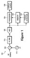
- FIG. 1 depicts a high-level block diagram of a real-time spectrum analyzer.
- FIG. 2 depicts a high-level functional block diagram of the processor shown in FIG. 1 .
- FIG. 3 depicts a flowchart of a method according to an embodiment of the present invention.
- FIG. 4 depicts a first bitmap
- FIG. 5 depicts a second bitmap
- FIG. 6 depicts a difference bitmap
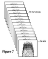
- FIG. 7 depicts a visualization of a first manner of updating a reference bitmap.
- FIG. 8 depicts two views of a visualization of a second manner of updating a reference bitmap.
- FIG. 9 illustrates how a column of a reference bitmap is subtracted from a column of a bitmap under test to produce a column of a difference bitmap.
- a real-time spectrum analyzer 100 receives a radio frequency (RF) input signal and optionally down-converts it using a mixer 105 , local oscillator (LO) 110 , and filter 115 to produce an intermediate frequency (IF) signal.
- An analog-to-digital converter (ADC) 120 digitizes the IF signal to produce a continuous stream of digital data that represents the IF signal.
- the digital data is processed in two paths. In the first path, the digital data is input to a processor 125 that analyzes the digital data in real-time.
- the digital data is input to a memory 135 (which, in some embodiments, comprises a circular buffer) and also input to a trigger detector 140 that processes the digital data in real-time and compares the processed data to a user-specified trigger criterion.
- a trigger detector 140 When the processed digital data satisfies the trigger criterion, the trigger detector 140 generates a trigger signal that causes the memory 135 to store a block of digital data.
- the processor 125 analyzes the stored digital data. After processing by processor 125 , the digital data may be displayed on the display device 130 or stored in a storage device (not shown).
- the processor 125 uses a frequency transform 205 such as a fast Fourier transform (FFT), a chirp-Z transform, or the like to transform the continuous stream of digital data into a series of frequency spectra 210 in real-time.
- the spectra 210 are then accumulated in a data structure referred to as a "bitmap database” 220 , sometimes referred to herein as a "density bitmap” or alternatively as a "bitmap.”
- the spectra 210 may be accumulated in various ways. In one embodiment, each spectrum 210 is rasterized to produce a "rasterized spectrum" 215 .
- a rasterized spectrum comprises an array of cells arranged in of a series of rows and columns, with each row representing a particular amplitude value and each column representing a particular frequency value.
- the value of each cell is either a "1,” also referred to as a "hit,” which indicates that the input signal was present at that particular location in the amplitude versus frequency space during the measurement period, or a "0" (depicted as a blank cell), which indicates that it was not.
- the values of the corresponding cells of the rasterized spectra 215 are summed together to form the bitmap database 220 , and then the value of each cell of the bitmap database 220 is divided by the total number of rasterized spectra 215 so that it indicates the total number of hits during the measurement period divided by the total number of rasterized spectra 215 , or equivalently, the percentage of time during the measurement period that the input signal occupied that particular location in the amplitude versus frequency space, also referred to as "DPX Density ® " or alternatively "density.”
- the rasterized spectra 215 and the bitmap database 220 are depicted as having ten rows and eleven columns for simplicity, however it will be appreciated that in an actual embodiment, the rasterized spectra 215 and the bitmap database 220 may have hundreds of rows and columns.
- the bitmap database 220 is essentially a three-dimensional histogram, with the x-axis being frequency, the y-axis being amplitude, and the z-axis being density.
- the bitmap database 220 may be displayed on the display device 145 with the density of each cell being represented by a color-graded pixel. Alternatively, the bitmap database 220 may be stored in a storage device (not shown).
- the series of frequency spectra 210 is converted into a plurality of bitmap databases 220 by organizing the series of frequency spectra 210 into sets of one or more frequency spectra 210 referred to as "frames" and then converting each frame into a bitmap database 220 .
- the processor 125 processes the digital data by performing the steps of ( 1 ) converting the digital data into a plurality of bitmaps and ( 2 ) subtracting one of the bitmaps referred to as a "reference bitmap” from another one of the bitmaps referred to as a "bitmap under test” to produce a "difference bitmap.”
- the difference bitmap does not contain the density values that are common to the two bitmaps, but instead only contains the density differences between the two.
- bitmap 400 shown in FIG. 4 and the bitmap 500 shown in FIG. 5 .
- Both bitmaps 400 and 500 were created from the same stream of digital data but at different times.
- the bitmaps 400 and 500 are depicted as having hundreds of rows and columns, the gridlines of which are not shown, and the color-grading of which is depicted as grey-scale with darker shades of grey indicating that the signal was present more often.
- Both bitmaps 400 and 500 depict a Quadrature Phase Shift Keying (QPSK) signal.
- QPSK Quadrature Phase Shift Keying
- the darkest density values indicate that the QPSK signal was present at that location in the power or amplitude versus frequency space a significant portion of the time during the measurement interval. Note that the bitmap 400 appears to be virtually identical to the bitmap 500 .
- Subtracting the bitmap 400 from the bitmap 500 produces a difference bitmap 600 as shown in FIG. 6 , where the color scaling is expanded to show a smaller range of density difference values, including both positive and negative density differences.
- the difference bitmap 600 reveals an interference signal 605 that is 20 dB below the QPSK signal.
- the interference signal 605 was present in bitmap 500 but not in bitmap 400 . Note that the interference signal 605 can be easily seen even though its peak density value is only 0.00002% (i.e., 20 micro-percent), in contrast to the QPSK signal which was present a significant portion of the time.
- the processor 125 converts the continuous stream of digital data is into a series of bitmaps in real-time and subtracts a reference bitmap from each newly created bitmap, thereby monitoring the input signal for very small density variations in real-time.
- the test and measurement instrument can "track-out" slow changes in the input signal, and thereby detect only changes that occur more quickly than the reference bitmap is updated. For example, if the reference bitmap is updated every 50 milliseconds, then, first order, the difference bitmap will only reveal changes in the input signal that occur within 50 milliseconds.
- the reference bitmap may be updated in various ways. In some embodiments, the reference bitmap is updated in response to a user command. In other embodiments, the reference bitmap is updated in response to a signal that is generated internally or externally to the real-time spectrum analyzer 100 .
- the processor 125 updates the reference bitmap periodically.
- the reference bitmap may be updated periodically in various ways.
- the reference bitmap is updated after each bitmap is created. This can be accomplished by storing new bitmaps as they are created in a First-In, First-Out (FIFO) memory structure, with the reference bitmap being whatever bitmap happens to be stored in a user-specified slot of the FIFO.
- FIG. 7 depicts a visualization of an example of this embodiment in which thirteen bitmaps are stored in a FIFO.
- the user-specified slot is the tenth slot, and thus the reference bitmap 710 is whatever bitmap happens to be stored in the tenth slot.
- the reference bitmap 710 is always ten bitmaps prior to the newly-created bitmap 700 .
- the reference bitmap "rolls" through time at the same rate that new bitmaps are created.
- the reference bitmap is updated after every N bitmaps is created, where N is a user-specified integer greater than one.
- the reference bitmap may be updated with a more recently created bitmap after every ten bitmaps is created. In that case, after the reference bitmap is updated, it is subtracted from the next ten bitmaps to generate ten difference bitmaps, and then the reference bitmap would be updated again.
- This manner of updating the reference bitmap can also be visualized in terms of a FIFO. For example, FIG.
- FIG. 8 shows two views of the same FIFO at two different times, one in which the reference bitmap 805 is five bitmaps prior to the newly created bitmap 800 , and one in which the reference bitmap 810 is ten bitmaps prior to the newly created bitmap 800 , with the other slots of the FIFO being empty. It will be appreciated that this method of updating the reference bitmap advantageously reduces the amount of memory required to store bitmaps compared to the method described in the previous paragraph.
- the difference bitmap may be processed in order to make density differences easier to see by applying smoothing, filtering, emphasizing density differences above a user-specified value, de-emphasizing density differences below a user-specified value, and so on.
- smoothing, filtering, emphasizing density differences above a user-specified value, de-emphasizing density differences below a user-specified value, and so on it may be advantageous to apply persistence so that a brief transient signal remains visible on the display device 130 long enough for a user to observe it.
- a difference bitmap is used to perform a measurement. It will be appreciated that a difference bitmap may be used to perform many of the measurements that are available on a real-time spectrum analyzer that normally operate on a conventional bitmap, although the results of those measurements may have significantly different meanings.
- the processor 125 collects a plurality of sequential bitmaps, subtracts the plurality of sequential bitmaps from a single reference bitmap to produce a plurality of difference bitmaps that represent a plurality of different measurement intervals, measures the density differences of each of the difference bitmaps to produce a plurality of density difference measurements, and then provides those density difference measurements in the form of a display of density difference versus measurement interval. In this manner, the processor 125 may help a user identify the period of intermittent interference signals present in the input signal.
- a positive density difference indicates that the bitmap under test had more hits at that location than the reference bitmap, meaning that the input signal spent more time at that particular amplitude and less time at a higher or lower amplitude.
- a positive density difference located above a negative density difference indicates that the bitmap under test depicts a signal that is not present in the reference bitmap, or in other words, it indicates that the signal "appeared.”
- a positive density difference located below a negative density difference indicates that the reference bitmap depicts a signal that is not present in the bitmap under test, or in other words, it indicates that the signal "disappeared.” This is because, when an additional signal of any kind is introduced into a frequency band, it increases the total power level in that frequency band. Conversely, when a signal is removed from a frequency band, it decreases the total power level in that frequency band.
- the mean of the noise distribution which is indicated by the pixel containing nine hits, is located nine pixels from the top of the column 910 .
- the column 905 which represents one column of a bitmap under test. There, an additional signal has been introduced into the frequency band which increases the total power in the frequency band by the power of the additional signal, or in other words, it shifts the noise distribution vertically by two pixels. Thus, the mean of the noise distribution is now located seven pixels from the top of the column 905 .
- the column 915 represents one column of a difference bitmap, formed by subtracting the column 910 of the reference bitmap from the column 905 of the bitmap under test.
- a positive density difference (2) located above a negative density difference (-5) indicates that the additional signal "appeared.”
- the pattern reverses when the additional signal is present in the reference bitmap but not present in the bitmap under test, producing positive density differences at lower amplitudes and negative density differences at higher amplitudes.
- the processor 125 indicates when a signal appears or disappears within the difference bitmap. In other embodiments, the processor 125 indicates when a signal appears or disappears within a user-specified portion of the difference bitmap.
- the trigger detector 140 processes the digital data by performing the steps of ( 1 ) converting the digital data into a plurality of bitmaps and ( 2 ) subtracting one of the bitmaps referred to as a "reference bitmap” from another one of the bitmaps referred to as a "bitmap under test” to produce a "difference bitmap.”
- the difference bitmap satisfies a user-specified trigger criterion
- the trigger detector 140 generates a trigger signal.
- the trigger signal causes the memory 135 to store a block of digital data, which are then analyzed by the processor 125 , and the results may be displayed on the display device 130 or stored in a storage device (not shown).
- the user-specified trigger criterion can take many forms.
- the trigger detector 140 generates the trigger signal when the peak density difference within the difference bitmap exceeds a user-specified density threshold.
- the trigger detector 140 generates the trigger signal when the peak density difference within a user-specified portion of the difference bitmap exceeds a user-specified density threshold.
- the difference bitmap is used in the place of a conventional bitmap in any one of various triggering schemes that trigger based on conventional bitmaps and the user-specified trigger criterion is defined by those triggering schemes. Examples of such triggering schemes include co-pending U.S. Patent Application No.
- the processor 125 and the trigger detector 140 may be implemented in hardware, software, or a combination of the two, and may comprise and/or be executed on a general purpose microprocessor, a digital signal processor (DSP), an application specific integrated circuit (ASIC), a field-programmable gate array (FPGA), or the like.
- DSP digital signal processor
- ASIC application specific integrated circuit
- FPGA field-programmable gate array
- an oscilloscope converts digital data that represents an input signal into a plurality of eye diagrams, and then subtracts one of the eye diagrams from another one of the eye diagrams to produce a difference eye diagram that reveals very small intermittent signals that are present in the input signal.
- the bitmap is not a frequency-domain bitmap as described above, but rather represents an accumulation of sampled voltage values in the time-domain.
Landscapes
- Physics & Mathematics (AREA)
- General Physics & Mathematics (AREA)
- Testing, Inspecting, Measuring Of Stereoscopic Televisions And Televisions (AREA)
- Spectrometry And Color Measurement (AREA)
- Tests Of Electronic Circuits (AREA)
- Controls And Circuits For Display Device (AREA)
- Image Processing (AREA)
Applications Claiming Priority (2)
| Application Number | Priority Date | Filing Date | Title |
|---|---|---|---|
| US33212310P | 2010-05-06 | 2010-05-06 | |
| US12/790,403 US8706435B2 (en) | 2010-05-06 | 2010-05-28 | Signal detection and triggering using a difference bitmap |
Publications (3)
| Publication Number | Publication Date |
|---|---|
| EP2385379A2 true EP2385379A2 (fr) | 2011-11-09 |
| EP2385379A3 EP2385379A3 (fr) | 2013-03-13 |
| EP2385379B1 EP2385379B1 (fr) | 2019-06-12 |
Family
ID=44477656
Family Applications (1)
| Application Number | Title | Priority Date | Filing Date |
|---|---|---|---|
| EP11161421.0A Active EP2385379B1 (fr) | 2010-05-06 | 2011-04-07 | Détection de signal et déclenchement utilisant un bitmap de différence |
Country Status (4)
| Country | Link |
|---|---|
| US (1) | US8706435B2 (fr) |
| EP (1) | EP2385379B1 (fr) |
| JP (1) | JP5858354B2 (fr) |
| CN (1) | CN102313841B (fr) |
Cited By (2)
| Publication number | Priority date | Publication date | Assignee | Title |
|---|---|---|---|---|
| EP2667204A1 (fr) * | 2012-05-24 | 2013-11-27 | Tektronix, Inc. | Déclenchement de domaine temporel dans un instrument de mesure et de test |
| WO2014072271A1 (fr) * | 2012-11-12 | 2014-05-15 | Rohde & Schwarz Gmbh & Co. Kg | Procédé et dispositif de détermination d'une condition de déclenchement d'un événement de signalisation rare |
Families Citing this family (9)
| Publication number | Priority date | Publication date | Assignee | Title |
|---|---|---|---|---|
| US8489350B2 (en) * | 2009-03-13 | 2013-07-16 | Tektronix, Inc. | Frequency domain bitmap triggering using color, density and correlation based triggers |
| US8880369B2 (en) | 2009-03-13 | 2014-11-04 | Tektronix, Inc. | Occupancy measurement and triggering in frequency domain bitmaps |
| US8364033B2 (en) * | 2009-12-08 | 2013-01-29 | Telcordia Technologies, Inc. | Differential eye diagrams |
| US8705598B2 (en) * | 2011-12-15 | 2014-04-22 | Tektronix, Inc. | Signal-sensitive data compression |
| US20130226500A1 (en) * | 2012-02-27 | 2013-08-29 | Yazaki North America, Inc. | Determination of validity of bi-level digital signal via digital data acquisition |
| JP6356737B2 (ja) * | 2016-07-04 | 2018-07-11 | アンリツ株式会社 | 信号解析装置及び信号解析方法 |
| CN112136054B (zh) * | 2018-05-25 | 2023-06-13 | 株式会社东阳特克尼卡 | 频谱分析方法、其装置以及记录介质 |
| CN113760915B (zh) * | 2021-09-07 | 2024-07-19 | 百果园技术(新加坡)有限公司 | 一种数据处理方法、装置、设备及介质 |
| CN118628596B (zh) * | 2024-05-24 | 2026-02-13 | 西安电子科技大学 | 一种基于数字余晖图的高隐蔽信号检测方法、系统、设备和介质 |
Family Cites Families (21)
| Publication number | Priority date | Publication date | Assignee | Title |
|---|---|---|---|---|
| US5426506A (en) * | 1993-03-22 | 1995-06-20 | The University Of Chicago | Optical method and apparatus for detection of surface and near-subsurface defects in dense ceramics |
| JP3370796B2 (ja) * | 1994-10-14 | 2003-01-27 | 富士写真フイルム株式会社 | 画像異常検出方法および装置 |
| JPH11298890A (ja) * | 1998-04-13 | 1999-10-29 | Hitachi Ltd | 画像データの圧縮又は伸張方法とその装置、並びに、それを用いた画像伝送システム及び監視システム |
| SE9801367L (sv) * | 1998-04-20 | 1999-09-27 | Ericsson Telefon Ab L M | Analog till digital omvandling med succesiv approximation |
| US6163758A (en) * | 1998-06-05 | 2000-12-19 | Tektronix, Inc. | Detection of unusual waveforms |
| JP3730435B2 (ja) * | 1999-03-26 | 2006-01-05 | 株式会社東芝 | 波形信号解析装置 |
| US6493400B1 (en) | 1999-04-19 | 2002-12-10 | Bae Systems Aerospace Electronics Inc. | Harmonic cancellation system |
| US6570592B1 (en) * | 1999-10-29 | 2003-05-27 | Agilent Technologies, Inc. | System and method for specifying trigger conditions of a signal measurement system using graphical elements on a graphical user interface |
| US6615369B1 (en) | 2000-01-31 | 2003-09-02 | Agilent Technologies, Inc. | Logic analyzer with trigger specification defined by waveform exemplar |
| JP4813774B2 (ja) | 2004-05-18 | 2011-11-09 | テクトロニクス・インターナショナル・セールス・ゲーエムベーハー | 周波数分析装置の表示方法 |
| US7251577B2 (en) * | 2004-07-19 | 2007-07-31 | Tektronix, Inc. | Realtime power mask trigger |
| WO2006072255A1 (fr) | 2005-01-10 | 2006-07-13 | Navico Danmark A/S | Systeme radar numerique a reduction d'echos parasites |
| US7359810B2 (en) | 2005-03-18 | 2008-04-15 | Tektronix, Inc. | Characterizing newly acquired waveforms for identification of waveform anomalies |
| US20070061629A1 (en) | 2005-08-15 | 2007-03-15 | Thums Eric E | Drop and drag logic analyzer trigger |
| US20070282542A1 (en) | 2006-05-31 | 2007-12-06 | Duff Christopher P | Composite trigger for a digital sampling oscilloscope |
| JP5194390B2 (ja) * | 2006-06-21 | 2013-05-08 | 株式会社リコー | データ処理装置 |
| JP5705395B2 (ja) * | 2006-07-21 | 2015-04-22 | テクトロニクス・インターナショナル・セールス・ゲーエムベーハー | 信号分析装置 |
| GB2455052A (en) * | 2007-09-21 | 2009-06-03 | Agilent Technologies Inc | Trigger event detection apparatus and method therefore |
| US7983332B2 (en) | 2007-11-12 | 2011-07-19 | Tektronix, Inc. | Eye violation and excess jitter trigger |
| JP2011523706A (ja) | 2008-05-22 | 2011-08-18 | テクトロニクス・インコーポレイテッド | 3次元ビットマップでの信号検索 |
| US8090184B2 (en) * | 2008-07-23 | 2012-01-03 | Seiko Epson Corporation | Fault detection of a printed dot-pattern bitmap |
-
2010
- 2010-05-28 US US12/790,403 patent/US8706435B2/en active Active
-
2011
- 2011-04-07 EP EP11161421.0A patent/EP2385379B1/fr active Active
- 2011-04-11 JP JP2011087274A patent/JP5858354B2/ja active Active
- 2011-05-06 CN CN201110125798.9A patent/CN102313841B/zh active Active
Non-Patent Citations (1)
| Title |
|---|
| None |
Cited By (3)
| Publication number | Priority date | Publication date | Assignee | Title |
|---|---|---|---|---|
| EP2667204A1 (fr) * | 2012-05-24 | 2013-11-27 | Tektronix, Inc. | Déclenchement de domaine temporel dans un instrument de mesure et de test |
| WO2014072271A1 (fr) * | 2012-11-12 | 2014-05-15 | Rohde & Schwarz Gmbh & Co. Kg | Procédé et dispositif de détermination d'une condition de déclenchement d'un événement de signalisation rare |
| US9759747B2 (en) | 2012-11-12 | 2017-09-12 | Rohde & Schwarz Gmbh & Co. Kg | Method and a device for determining a trigger condition for a rare signal event |
Also Published As
| Publication number | Publication date |
|---|---|
| EP2385379A3 (fr) | 2013-03-13 |
| JP5858354B2 (ja) | 2016-02-10 |
| US20110273469A1 (en) | 2011-11-10 |
| JP2011237414A (ja) | 2011-11-24 |
| CN102313841B (zh) | 2015-12-09 |
| CN102313841A (zh) | 2012-01-11 |
| EP2385379B1 (fr) | 2019-06-12 |
| US8706435B2 (en) | 2014-04-22 |
Similar Documents
| Publication | Publication Date | Title |
|---|---|---|
| EP2385379B1 (fr) | Détection de signal et déclenchement utilisant un bitmap de différence | |
| EP2605025B1 (fr) | Déclenchement de masque de fréquence avec segments de bande non uniformes | |
| EP2228660B1 (fr) | Déclenchement de bitmaps du domaine de fréquence à l'aide d'un déclenchement basé sur la couleur, la densité et la corrélation | |
| US10459008B2 (en) | Occupancy measurement and triggering in frequency domain bitmaps | |
| EP2386867B1 (fr) | Reconnaissance et déclenchement de signaux utilisant des techniques de vision informatique | |
| EP2402767B1 (fr) | Procédé et appareil pour générer un bitmap de densité à déclenchement périodique | |
| JP2010217179A (ja) | 試験測定装置及びそのトリガ動作方法 | |
| CN102037478A (zh) | 三维位图中的信号搜索 | |
| EP2386869B1 (fr) | Mesure et déclenchement de trace de densité dans des bitmaps du domaine de fréquence | |
| US7505039B2 (en) | Track of statistics | |
| EP2743709A1 (fr) | Analyseur de spectre en temps réel avec affichage de zoom | |
| US20130141466A1 (en) | Real time spectrum analyzer with zoom display | |
| JP6168763B2 (ja) | 試験測定装置及び試験測定装置における方法 | |
| EP2667204A1 (fr) | Déclenchement de domaine temporel dans un instrument de mesure et de test | |
| EP2520941A1 (fr) | Indicateur de déclenchement de facteur de mérite | |
| JP2014235150A (ja) | 試験測定装置及び画像生成方法 |
Legal Events
| Date | Code | Title | Description |
|---|---|---|---|
| AK | Designated contracting states |
Kind code of ref document: A2 Designated state(s): AL AT BE BG CH CY CZ DE DK EE ES FI FR GB GR HR HU IE IS IT LI LT LU LV MC MK MT NL NO PL PT RO RS SE SI SK SM TR |
|
| AX | Request for extension of the european patent |
Extension state: BA ME |
|
| PUAI | Public reference made under article 153(3) epc to a published international application that has entered the european phase |
Free format text: ORIGINAL CODE: 0009012 |
|
| PUAL | Search report despatched |
Free format text: ORIGINAL CODE: 0009013 |
|
| AK | Designated contracting states |
Kind code of ref document: A3 Designated state(s): AL AT BE BG CH CY CZ DE DK EE ES FI FR GB GR HR HU IE IS IT LI LT LU LV MC MK MT NL NO PL PT RO RS SE SI SK SM TR |
|
| AX | Request for extension of the european patent |
Extension state: BA ME |
|
| RIC1 | Information provided on ipc code assigned before grant |
Ipc: G01R 13/02 20060101AFI20130207BHEP |
|
| 17P | Request for examination filed |
Effective date: 20130620 |
|
| RBV | Designated contracting states (corrected) |
Designated state(s): AL AT BE BG CH CY CZ DE DK EE ES FI FR GB GR HR HU IE IS IT LI LT LU LV MC MK MT NL NO PL PT RO RS SE SI SK SM TR |
|
| RAP1 | Party data changed (applicant data changed or rights of an application transferred) |
Owner name: TEKTRONIX, INC. |
|
| STAA | Information on the status of an ep patent application or granted ep patent |
Free format text: STATUS: EXAMINATION IS IN PROGRESS |
|
| 17Q | First examination report despatched |
Effective date: 20180221 |
|
| GRAP | Despatch of communication of intention to grant a patent |
Free format text: ORIGINAL CODE: EPIDOSNIGR1 |
|
| STAA | Information on the status of an ep patent application or granted ep patent |
Free format text: STATUS: GRANT OF PATENT IS INTENDED |
|
| INTG | Intention to grant announced |
Effective date: 20181102 |
|
| GRAS | Grant fee paid |
Free format text: ORIGINAL CODE: EPIDOSNIGR3 |
|
| GRAA | (expected) grant |
Free format text: ORIGINAL CODE: 0009210 |
|
| STAA | Information on the status of an ep patent application or granted ep patent |
Free format text: STATUS: THE PATENT HAS BEEN GRANTED |
|
| AK | Designated contracting states |
Kind code of ref document: B1 Designated state(s): AL AT BE BG CH CY CZ DE DK EE ES FI FR GB GR HR HU IE IS IT LI LT LU LV MC MK MT NL NO PL PT RO RS SE SI SK SM TR |
|
| REG | Reference to a national code |
Ref country code: GB Ref legal event code: FG4D |
|
| REG | Reference to a national code |
Ref country code: CH Ref legal event code: EP |
|
| REG | Reference to a national code |
Ref country code: AT Ref legal event code: REF Ref document number: 1143255 Country of ref document: AT Kind code of ref document: T Effective date: 20190615 |
|
| REG | Reference to a national code |
Ref country code: DE Ref legal event code: R096 Ref document number: 602011059566 Country of ref document: DE |
|
| REG | Reference to a national code |
Ref country code: IE Ref legal event code: FG4D |
|
| REG | Reference to a national code |
Ref country code: NL Ref legal event code: MP Effective date: 20190612 |
|
| REG | Reference to a national code |
Ref country code: LT Ref legal event code: MG4D |
|
| PG25 | Lapsed in a contracting state [announced via postgrant information from national office to epo] |
Ref country code: AL Free format text: LAPSE BECAUSE OF FAILURE TO SUBMIT A TRANSLATION OF THE DESCRIPTION OR TO PAY THE FEE WITHIN THE PRESCRIBED TIME-LIMIT Effective date: 20190612 Ref country code: ES Free format text: LAPSE BECAUSE OF FAILURE TO SUBMIT A TRANSLATION OF THE DESCRIPTION OR TO PAY THE FEE WITHIN THE PRESCRIBED TIME-LIMIT Effective date: 20190612 Ref country code: SE Free format text: LAPSE BECAUSE OF FAILURE TO SUBMIT A TRANSLATION OF THE DESCRIPTION OR TO PAY THE FEE WITHIN THE PRESCRIBED TIME-LIMIT Effective date: 20190612 Ref country code: NO Free format text: LAPSE BECAUSE OF FAILURE TO SUBMIT A TRANSLATION OF THE DESCRIPTION OR TO PAY THE FEE WITHIN THE PRESCRIBED TIME-LIMIT Effective date: 20190912 Ref country code: FI Free format text: LAPSE BECAUSE OF FAILURE TO SUBMIT A TRANSLATION OF THE DESCRIPTION OR TO PAY THE FEE WITHIN THE PRESCRIBED TIME-LIMIT Effective date: 20190612 Ref country code: HR Free format text: LAPSE BECAUSE OF FAILURE TO SUBMIT A TRANSLATION OF THE DESCRIPTION OR TO PAY THE FEE WITHIN THE PRESCRIBED TIME-LIMIT Effective date: 20190612 Ref country code: LT Free format text: LAPSE BECAUSE OF FAILURE TO SUBMIT A TRANSLATION OF THE DESCRIPTION OR TO PAY THE FEE WITHIN THE PRESCRIBED TIME-LIMIT Effective date: 20190612 |
|
| PG25 | Lapsed in a contracting state [announced via postgrant information from national office to epo] |
Ref country code: RS Free format text: LAPSE BECAUSE OF FAILURE TO SUBMIT A TRANSLATION OF THE DESCRIPTION OR TO PAY THE FEE WITHIN THE PRESCRIBED TIME-LIMIT Effective date: 20190612 Ref country code: GR Free format text: LAPSE BECAUSE OF FAILURE TO SUBMIT A TRANSLATION OF THE DESCRIPTION OR TO PAY THE FEE WITHIN THE PRESCRIBED TIME-LIMIT Effective date: 20190913 Ref country code: BG Free format text: LAPSE BECAUSE OF FAILURE TO SUBMIT A TRANSLATION OF THE DESCRIPTION OR TO PAY THE FEE WITHIN THE PRESCRIBED TIME-LIMIT Effective date: 20190912 Ref country code: LV Free format text: LAPSE BECAUSE OF FAILURE TO SUBMIT A TRANSLATION OF THE DESCRIPTION OR TO PAY THE FEE WITHIN THE PRESCRIBED TIME-LIMIT Effective date: 20190612 |
|
| REG | Reference to a national code |
Ref country code: AT Ref legal event code: MK05 Ref document number: 1143255 Country of ref document: AT Kind code of ref document: T Effective date: 20190612 |
|
| PG25 | Lapsed in a contracting state [announced via postgrant information from national office to epo] |
Ref country code: PT Free format text: LAPSE BECAUSE OF FAILURE TO SUBMIT A TRANSLATION OF THE DESCRIPTION OR TO PAY THE FEE WITHIN THE PRESCRIBED TIME-LIMIT Effective date: 20191014 Ref country code: EE Free format text: LAPSE BECAUSE OF FAILURE TO SUBMIT A TRANSLATION OF THE DESCRIPTION OR TO PAY THE FEE WITHIN THE PRESCRIBED TIME-LIMIT Effective date: 20190612 Ref country code: NL Free format text: LAPSE BECAUSE OF FAILURE TO SUBMIT A TRANSLATION OF THE DESCRIPTION OR TO PAY THE FEE WITHIN THE PRESCRIBED TIME-LIMIT Effective date: 20190612 Ref country code: CZ Free format text: LAPSE BECAUSE OF FAILURE TO SUBMIT A TRANSLATION OF THE DESCRIPTION OR TO PAY THE FEE WITHIN THE PRESCRIBED TIME-LIMIT Effective date: 20190612 Ref country code: RO Free format text: LAPSE BECAUSE OF FAILURE TO SUBMIT A TRANSLATION OF THE DESCRIPTION OR TO PAY THE FEE WITHIN THE PRESCRIBED TIME-LIMIT Effective date: 20190612 Ref country code: AT Free format text: LAPSE BECAUSE OF FAILURE TO SUBMIT A TRANSLATION OF THE DESCRIPTION OR TO PAY THE FEE WITHIN THE PRESCRIBED TIME-LIMIT Effective date: 20190612 Ref country code: SK Free format text: LAPSE BECAUSE OF FAILURE TO SUBMIT A TRANSLATION OF THE DESCRIPTION OR TO PAY THE FEE WITHIN THE PRESCRIBED TIME-LIMIT Effective date: 20190612 |
|
| PG25 | Lapsed in a contracting state [announced via postgrant information from national office to epo] |
Ref country code: IS Free format text: LAPSE BECAUSE OF FAILURE TO SUBMIT A TRANSLATION OF THE DESCRIPTION OR TO PAY THE FEE WITHIN THE PRESCRIBED TIME-LIMIT Effective date: 20191012 Ref country code: SM Free format text: LAPSE BECAUSE OF FAILURE TO SUBMIT A TRANSLATION OF THE DESCRIPTION OR TO PAY THE FEE WITHIN THE PRESCRIBED TIME-LIMIT Effective date: 20190612 Ref country code: IT Free format text: LAPSE BECAUSE OF FAILURE TO SUBMIT A TRANSLATION OF THE DESCRIPTION OR TO PAY THE FEE WITHIN THE PRESCRIBED TIME-LIMIT Effective date: 20190612 |
|
| REG | Reference to a national code |
Ref country code: DE Ref legal event code: R097 Ref document number: 602011059566 Country of ref document: DE |
|
| PG25 | Lapsed in a contracting state [announced via postgrant information from national office to epo] |
Ref country code: TR Free format text: LAPSE BECAUSE OF FAILURE TO SUBMIT A TRANSLATION OF THE DESCRIPTION OR TO PAY THE FEE WITHIN THE PRESCRIBED TIME-LIMIT Effective date: 20190612 |
|
| PLBE | No opposition filed within time limit |
Free format text: ORIGINAL CODE: 0009261 |
|
| STAA | Information on the status of an ep patent application or granted ep patent |
Free format text: STATUS: NO OPPOSITION FILED WITHIN TIME LIMIT |
|
| PG25 | Lapsed in a contracting state [announced via postgrant information from national office to epo] |
Ref country code: DK Free format text: LAPSE BECAUSE OF FAILURE TO SUBMIT A TRANSLATION OF THE DESCRIPTION OR TO PAY THE FEE WITHIN THE PRESCRIBED TIME-LIMIT Effective date: 20190612 Ref country code: PL Free format text: LAPSE BECAUSE OF FAILURE TO SUBMIT A TRANSLATION OF THE DESCRIPTION OR TO PAY THE FEE WITHIN THE PRESCRIBED TIME-LIMIT Effective date: 20190612 |
|
| 26N | No opposition filed |
Effective date: 20200313 |
|
| PG25 | Lapsed in a contracting state [announced via postgrant information from national office to epo] |
Ref country code: IS Free format text: LAPSE BECAUSE OF FAILURE TO SUBMIT A TRANSLATION OF THE DESCRIPTION OR TO PAY THE FEE WITHIN THE PRESCRIBED TIME-LIMIT Effective date: 20200224 Ref country code: SI Free format text: LAPSE BECAUSE OF FAILURE TO SUBMIT A TRANSLATION OF THE DESCRIPTION OR TO PAY THE FEE WITHIN THE PRESCRIBED TIME-LIMIT Effective date: 20190612 |
|
| PG2D | Information on lapse in contracting state deleted |
Ref country code: IS |
|
| PG25 | Lapsed in a contracting state [announced via postgrant information from national office to epo] |
Ref country code: IS Free format text: LAPSE BECAUSE OF FAILURE TO SUBMIT A TRANSLATION OF THE DESCRIPTION OR TO PAY THE FEE WITHIN THE PRESCRIBED TIME-LIMIT Effective date: 20191112 |
|
| PG25 | Lapsed in a contracting state [announced via postgrant information from national office to epo] |
Ref country code: MC Free format text: LAPSE BECAUSE OF FAILURE TO SUBMIT A TRANSLATION OF THE DESCRIPTION OR TO PAY THE FEE WITHIN THE PRESCRIBED TIME-LIMIT Effective date: 20190612 |
|
| REG | Reference to a national code |
Ref country code: CH Ref legal event code: PL |
|
| PG25 | Lapsed in a contracting state [announced via postgrant information from national office to epo] |
Ref country code: LU Free format text: LAPSE BECAUSE OF NON-PAYMENT OF DUE FEES Effective date: 20200407 Ref country code: FR Free format text: LAPSE BECAUSE OF NON-PAYMENT OF DUE FEES Effective date: 20200430 Ref country code: LI Free format text: LAPSE BECAUSE OF NON-PAYMENT OF DUE FEES Effective date: 20200430 Ref country code: CH Free format text: LAPSE BECAUSE OF NON-PAYMENT OF DUE FEES Effective date: 20200430 |
|
| REG | Reference to a national code |
Ref country code: BE Ref legal event code: MM Effective date: 20200430 |
|
| PG25 | Lapsed in a contracting state [announced via postgrant information from national office to epo] |
Ref country code: BE Free format text: LAPSE BECAUSE OF NON-PAYMENT OF DUE FEES Effective date: 20200430 |
|
| GBPC | Gb: european patent ceased through non-payment of renewal fee |
Effective date: 20200407 |
|
| PG25 | Lapsed in a contracting state [announced via postgrant information from national office to epo] |
Ref country code: IE Free format text: LAPSE BECAUSE OF NON-PAYMENT OF DUE FEES Effective date: 20200407 Ref country code: GB Free format text: LAPSE BECAUSE OF NON-PAYMENT OF DUE FEES Effective date: 20200407 |
|
| PG25 | Lapsed in a contracting state [announced via postgrant information from national office to epo] |
Ref country code: MT Free format text: LAPSE BECAUSE OF FAILURE TO SUBMIT A TRANSLATION OF THE DESCRIPTION OR TO PAY THE FEE WITHIN THE PRESCRIBED TIME-LIMIT Effective date: 20190612 Ref country code: CY Free format text: LAPSE BECAUSE OF FAILURE TO SUBMIT A TRANSLATION OF THE DESCRIPTION OR TO PAY THE FEE WITHIN THE PRESCRIBED TIME-LIMIT Effective date: 20190612 |
|
| PG25 | Lapsed in a contracting state [announced via postgrant information from national office to epo] |
Ref country code: MK Free format text: LAPSE BECAUSE OF FAILURE TO SUBMIT A TRANSLATION OF THE DESCRIPTION OR TO PAY THE FEE WITHIN THE PRESCRIBED TIME-LIMIT Effective date: 20190612 |
|
| P01 | Opt-out of the competence of the unified patent court (upc) registered |
Effective date: 20230530 |
|
| PGFP | Annual fee paid to national office [announced via postgrant information from national office to epo] |
Ref country code: DE Payment date: 20250428 Year of fee payment: 15 |