EP2385420A1 - Dispositif d'affichage à cristaux liquides et procédé pour sa fabrication - Google Patents
Dispositif d'affichage à cristaux liquides et procédé pour sa fabrication Download PDFInfo
- Publication number
- EP2385420A1 EP2385420A1 EP10735749A EP10735749A EP2385420A1 EP 2385420 A1 EP2385420 A1 EP 2385420A1 EP 10735749 A EP10735749 A EP 10735749A EP 10735749 A EP10735749 A EP 10735749A EP 2385420 A1 EP2385420 A1 EP 2385420A1
- Authority
- EP
- European Patent Office
- Prior art keywords
- liquid crystal
- side chain
- crystal display
- compound
- group
- Prior art date
- Legal status (The legal status is an assumption and is not a legal conclusion. Google has not performed a legal analysis and makes no representation as to the accuracy of the status listed.)
- Withdrawn
Links
- 0 C**(C)(C)C(CC1)C(C)(CC2)C1C(CC1)C2C(C)(CC2)C1CC2(c(cc1)ccc1Oc1ccc(C)cc1)c(cc1)ccc1Oc1ccc(C)cc1 Chemical compound C**(C)(C)C(CC1)C(C)(CC2)C1C(CC1)C2C(C)(CC2)C1CC2(c(cc1)ccc1Oc1ccc(C)cc1)c(cc1)ccc1Oc1ccc(C)cc1 0.000 description 10
- HKKGIHCPNBYMFD-UHFFFAOYSA-N C1=CC=[I]C=C1 Chemical compound C1=CC=[I]C=C1 HKKGIHCPNBYMFD-UHFFFAOYSA-N 0.000 description 1
- ITSMGJSJUFXJLX-AATRIKPKSA-N CC(C)C1C=CC(/C=C/C=C)=CC1 Chemical compound CC(C)C1C=CC(/C=C/C=C)=CC1 ITSMGJSJUFXJLX-AATRIKPKSA-N 0.000 description 1
- WSWPHHNIHLTAHB-UHFFFAOYSA-N CCOc1ccc(C)cc1 Chemical compound CCOc1ccc(C)cc1 WSWPHHNIHLTAHB-UHFFFAOYSA-N 0.000 description 1
- IFKBYZUWKXQXSM-UHFFFAOYSA-N CCc1ccc(C2C3C2C3)cc1 Chemical compound CCc1ccc(C2C3C2C3)cc1 IFKBYZUWKXQXSM-UHFFFAOYSA-N 0.000 description 1
- YXFVVABEGXRONW-UHFFFAOYSA-N Cc1ccccc1 Chemical compound Cc1ccccc1 YXFVVABEGXRONW-UHFFFAOYSA-N 0.000 description 1
- SETXVYAPNOMCAP-UHFFFAOYSA-N OC(c1cc(C(c(cccc2C(O3)=O)c2C3=O)=O)ccc11)OC1=O Chemical compound OC(c1cc(C(c(cccc2C(O3)=O)c2C3=O)=O)ccc11)OC1=O SETXVYAPNOMCAP-UHFFFAOYSA-N 0.000 description 1
Images







Classifications
-
- G—PHYSICS
- G02—OPTICS
- G02F—OPTICAL DEVICES OR ARRANGEMENTS FOR THE CONTROL OF LIGHT BY MODIFICATION OF THE OPTICAL PROPERTIES OF THE MEDIA OF THE ELEMENTS INVOLVED THEREIN; NON-LINEAR OPTICS; FREQUENCY-CHANGING OF LIGHT; OPTICAL LOGIC ELEMENTS; OPTICAL ANALOGUE/DIGITAL CONVERTERS
- G02F1/00—Devices or arrangements for the control of the intensity, colour, phase, polarisation or direction of light arriving from an independent light source, e.g. switching, gating or modulating; Non-linear optics
- G02F1/01—Devices or arrangements for the control of the intensity, colour, phase, polarisation or direction of light arriving from an independent light source, e.g. switching, gating or modulating; Non-linear optics for the control of the intensity, phase, polarisation or colour
- G02F1/13—Devices or arrangements for the control of the intensity, colour, phase, polarisation or direction of light arriving from an independent light source, e.g. switching, gating or modulating; Non-linear optics for the control of the intensity, phase, polarisation or colour based on liquid crystals, e.g. single liquid crystal display cells
- G02F1/133—Constructional arrangements; Operation of liquid crystal cells; Circuit arrangements
- G02F1/1333—Constructional arrangements; Manufacturing methods
- G02F1/1337—Surface-induced orientation of the liquid crystal molecules, e.g. by alignment layers
- G02F1/133753—Surface-induced orientation of the liquid crystal molecules, e.g. by alignment layers with different alignment orientations or pretilt angles on a same surface, e.g. for grey scale or improved viewing angle
-
- G—PHYSICS
- G02—OPTICS
- G02F—OPTICAL DEVICES OR ARRANGEMENTS FOR THE CONTROL OF LIGHT BY MODIFICATION OF THE OPTICAL PROPERTIES OF THE MEDIA OF THE ELEMENTS INVOLVED THEREIN; NON-LINEAR OPTICS; FREQUENCY-CHANGING OF LIGHT; OPTICAL LOGIC ELEMENTS; OPTICAL ANALOGUE/DIGITAL CONVERTERS
- G02F1/00—Devices or arrangements for the control of the intensity, colour, phase, polarisation or direction of light arriving from an independent light source, e.g. switching, gating or modulating; Non-linear optics
- G02F1/01—Devices or arrangements for the control of the intensity, colour, phase, polarisation or direction of light arriving from an independent light source, e.g. switching, gating or modulating; Non-linear optics for the control of the intensity, phase, polarisation or colour
- G02F1/13—Devices or arrangements for the control of the intensity, colour, phase, polarisation or direction of light arriving from an independent light source, e.g. switching, gating or modulating; Non-linear optics for the control of the intensity, phase, polarisation or colour based on liquid crystals, e.g. single liquid crystal display cells
- G02F1/133—Constructional arrangements; Operation of liquid crystal cells; Circuit arrangements
- G02F1/1333—Constructional arrangements; Manufacturing methods
- G02F1/1337—Surface-induced orientation of the liquid crystal molecules, e.g. by alignment layers
- G02F1/133711—Surface-induced orientation of the liquid crystal molecules, e.g. by alignment layers by organic films, e.g. polymeric films
-
- C—CHEMISTRY; METALLURGY
- C07—ORGANIC CHEMISTRY
- C07C—ACYCLIC OR CARBOCYCLIC COMPOUNDS
- C07C49/00—Ketones; Ketenes; Dimeric ketenes; Ketonic chelates
- C07C49/76—Ketones containing a keto group bound to a six-membered aromatic ring
- C07C49/84—Ketones containing a keto group bound to a six-membered aromatic ring containing ether groups, groups, groups, or groups
-
- C—CHEMISTRY; METALLURGY
- C07—ORGANIC CHEMISTRY
- C07C—ACYCLIC OR CARBOCYCLIC COMPOUNDS
- C07C69/00—Esters of carboxylic acids; Esters of carbonic or haloformic acids
- C07C69/66—Esters of carboxylic acids having esterified carboxylic groups bound to acyclic carbon atoms and having any of the groups OH, O—metal, —CHO, keto, ether, acyloxy, groups, groups, or in the acid moiety
- C07C69/73—Esters of carboxylic acids having esterified carboxylic groups bound to acyclic carbon atoms and having any of the groups OH, O—metal, —CHO, keto, ether, acyloxy, groups, groups, or in the acid moiety of unsaturated acids
- C07C69/734—Ethers
- C07C69/736—Ethers the hydroxy group of the ester being etherified with a hydroxy compound having the hydroxy group bound to a carbon atom of a six-membered aromatic ring
-
- C—CHEMISTRY; METALLURGY
- C07—ORGANIC CHEMISTRY
- C07C—ACYCLIC OR CARBOCYCLIC COMPOUNDS
- C07C69/00—Esters of carboxylic acids; Esters of carbonic or haloformic acids
- C07C69/76—Esters of carboxylic acids having a carboxyl group bound to a carbon atom of a six-membered aromatic ring
-
- C—CHEMISTRY; METALLURGY
- C07—ORGANIC CHEMISTRY
- C07J—STEROIDS
- C07J9/00—Normal steroids containing carbon, hydrogen, halogen or oxygen substituted in position 17 beta by a chain of more than two carbon atoms, e.g. cholane, cholestane, coprostane
-
- C—CHEMISTRY; METALLURGY
- C07—ORGANIC CHEMISTRY
- C07J—STEROIDS
- C07J9/00—Normal steroids containing carbon, hydrogen, halogen or oxygen substituted in position 17 beta by a chain of more than two carbon atoms, e.g. cholane, cholestane, coprostane
- C07J9/005—Normal steroids containing carbon, hydrogen, halogen or oxygen substituted in position 17 beta by a chain of more than two carbon atoms, e.g. cholane, cholestane, coprostane containing a carboxylic function directly attached or attached by a chain containing only carbon atoms to the cyclopenta[a]hydrophenanthrene skeleton
-
- C—CHEMISTRY; METALLURGY
- C08—ORGANIC MACROMOLECULAR COMPOUNDS; THEIR PREPARATION OR CHEMICAL WORKING-UP; COMPOSITIONS BASED THEREON
- C08G—MACROMOLECULAR COMPOUNDS OBTAINED OTHERWISE THAN BY REACTIONS ONLY INVOLVING UNSATURATED CARBON-TO-CARBON BONDS
- C08G73/00—Macromolecular compounds obtained by reactions forming a linkage containing nitrogen with or without oxygen or carbon in the main chain of the macromolecule, not provided for in groups C08G12/00 - C08G71/00
- C08G73/06—Polycondensates having nitrogen-containing heterocyclic rings in the main chain of the macromolecule
- C08G73/10—Polyimides; Polyester-imides; Polyamide-imides; Polyamide acids or similar polyimide precursors
- C08G73/1075—Partially aromatic polyimides
-
- C—CHEMISTRY; METALLURGY
- C08—ORGANIC MACROMOLECULAR COMPOUNDS; THEIR PREPARATION OR CHEMICAL WORKING-UP; COMPOSITIONS BASED THEREON
- C08L—COMPOSITIONS OF MACROMOLECULAR COMPOUNDS
- C08L79/00—Compositions of macromolecular compounds obtained by reactions forming in the main chain of the macromolecule a linkage containing nitrogen with or without oxygen or carbon only, not provided for in groups C08L61/00 - C08L77/00
- C08L79/04—Polycondensates having nitrogen-containing heterocyclic rings in the main chain; Polyhydrazides; Polyamide acids or similar polyimide precursors
- C08L79/08—Polyimides; Polyester-imides; Polyamide-imides; Polyamide acids or similar polyimide precursors
-
- C—CHEMISTRY; METALLURGY
- C09—DYES; PAINTS; POLISHES; NATURAL RESINS; ADHESIVES; COMPOSITIONS NOT OTHERWISE PROVIDED FOR; APPLICATIONS OF MATERIALS NOT OTHERWISE PROVIDED FOR
- C09K—MATERIALS FOR MISCELLANEOUS APPLICATIONS, NOT PROVIDED FOR ELSEWHERE
- C09K19/00—Liquid crystal materials
- C09K19/52—Liquid crystal materials characterised by components which are not liquid crystals, e.g. additives with special physical aspect: solvents, solid particles
- C09K19/54—Additives having no specific mesophase characterised by their chemical composition
- C09K19/56—Aligning agents
-
- G—PHYSICS
- G02—OPTICS
- G02F—OPTICAL DEVICES OR ARRANGEMENTS FOR THE CONTROL OF LIGHT BY MODIFICATION OF THE OPTICAL PROPERTIES OF THE MEDIA OF THE ELEMENTS INVOLVED THEREIN; NON-LINEAR OPTICS; FREQUENCY-CHANGING OF LIGHT; OPTICAL LOGIC ELEMENTS; OPTICAL ANALOGUE/DIGITAL CONVERTERS
- G02F1/00—Devices or arrangements for the control of the intensity, colour, phase, polarisation or direction of light arriving from an independent light source, e.g. switching, gating or modulating; Non-linear optics
- G02F1/01—Devices or arrangements for the control of the intensity, colour, phase, polarisation or direction of light arriving from an independent light source, e.g. switching, gating or modulating; Non-linear optics for the control of the intensity, phase, polarisation or colour
- G02F1/13—Devices or arrangements for the control of the intensity, colour, phase, polarisation or direction of light arriving from an independent light source, e.g. switching, gating or modulating; Non-linear optics for the control of the intensity, phase, polarisation or colour based on liquid crystals, e.g. single liquid crystal display cells
- G02F1/133—Constructional arrangements; Operation of liquid crystal cells; Circuit arrangements
- G02F1/1333—Constructional arrangements; Manufacturing methods
- G02F1/1337—Surface-induced orientation of the liquid crystal molecules, e.g. by alignment layers
-
- G—PHYSICS
- G02—OPTICS
- G02F—OPTICAL DEVICES OR ARRANGEMENTS FOR THE CONTROL OF LIGHT BY MODIFICATION OF THE OPTICAL PROPERTIES OF THE MEDIA OF THE ELEMENTS INVOLVED THEREIN; NON-LINEAR OPTICS; FREQUENCY-CHANGING OF LIGHT; OPTICAL LOGIC ELEMENTS; OPTICAL ANALOGUE/DIGITAL CONVERTERS
- G02F1/00—Devices or arrangements for the control of the intensity, colour, phase, polarisation or direction of light arriving from an independent light source, e.g. switching, gating or modulating; Non-linear optics
- G02F1/01—Devices or arrangements for the control of the intensity, colour, phase, polarisation or direction of light arriving from an independent light source, e.g. switching, gating or modulating; Non-linear optics for the control of the intensity, phase, polarisation or colour
- G02F1/13—Devices or arrangements for the control of the intensity, colour, phase, polarisation or direction of light arriving from an independent light source, e.g. switching, gating or modulating; Non-linear optics for the control of the intensity, phase, polarisation or colour based on liquid crystals, e.g. single liquid crystal display cells
- G02F1/133—Constructional arrangements; Operation of liquid crystal cells; Circuit arrangements
- G02F1/1333—Constructional arrangements; Manufacturing methods
- G02F1/1337—Surface-induced orientation of the liquid crystal molecules, e.g. by alignment layers
- G02F1/133711—Surface-induced orientation of the liquid crystal molecules, e.g. by alignment layers by organic films, e.g. polymeric films
- G02F1/133715—Surface-induced orientation of the liquid crystal molecules, e.g. by alignment layers by organic films, e.g. polymeric films by first depositing a monomer
-
- G—PHYSICS
- G02—OPTICS
- G02F—OPTICAL DEVICES OR ARRANGEMENTS FOR THE CONTROL OF LIGHT BY MODIFICATION OF THE OPTICAL PROPERTIES OF THE MEDIA OF THE ELEMENTS INVOLVED THEREIN; NON-LINEAR OPTICS; FREQUENCY-CHANGING OF LIGHT; OPTICAL LOGIC ELEMENTS; OPTICAL ANALOGUE/DIGITAL CONVERTERS
- G02F1/00—Devices or arrangements for the control of the intensity, colour, phase, polarisation or direction of light arriving from an independent light source, e.g. switching, gating or modulating; Non-linear optics
- G02F1/01—Devices or arrangements for the control of the intensity, colour, phase, polarisation or direction of light arriving from an independent light source, e.g. switching, gating or modulating; Non-linear optics for the control of the intensity, phase, polarisation or colour
- G02F1/13—Devices or arrangements for the control of the intensity, colour, phase, polarisation or direction of light arriving from an independent light source, e.g. switching, gating or modulating; Non-linear optics for the control of the intensity, phase, polarisation or colour based on liquid crystals, e.g. single liquid crystal display cells
- G02F1/133—Constructional arrangements; Operation of liquid crystal cells; Circuit arrangements
- G02F1/1333—Constructional arrangements; Manufacturing methods
- G02F1/1337—Surface-induced orientation of the liquid crystal molecules, e.g. by alignment layers
- G02F1/133753—Surface-induced orientation of the liquid crystal molecules, e.g. by alignment layers with different alignment orientations or pretilt angles on a same surface, e.g. for grey scale or improved viewing angle
- G02F1/133761—Surface-induced orientation of the liquid crystal molecules, e.g. by alignment layers with different alignment orientations or pretilt angles on a same surface, e.g. for grey scale or improved viewing angle with different pretilt angles
-
- G—PHYSICS
- G02—OPTICS
- G02F—OPTICAL DEVICES OR ARRANGEMENTS FOR THE CONTROL OF LIGHT BY MODIFICATION OF THE OPTICAL PROPERTIES OF THE MEDIA OF THE ELEMENTS INVOLVED THEREIN; NON-LINEAR OPTICS; FREQUENCY-CHANGING OF LIGHT; OPTICAL LOGIC ELEMENTS; OPTICAL ANALOGUE/DIGITAL CONVERTERS
- G02F1/00—Devices or arrangements for the control of the intensity, colour, phase, polarisation or direction of light arriving from an independent light source, e.g. switching, gating or modulating; Non-linear optics
- G02F1/01—Devices or arrangements for the control of the intensity, colour, phase, polarisation or direction of light arriving from an independent light source, e.g. switching, gating or modulating; Non-linear optics for the control of the intensity, phase, polarisation or colour
- G02F1/13—Devices or arrangements for the control of the intensity, colour, phase, polarisation or direction of light arriving from an independent light source, e.g. switching, gating or modulating; Non-linear optics for the control of the intensity, phase, polarisation or colour based on liquid crystals, e.g. single liquid crystal display cells
- G02F1/133—Constructional arrangements; Operation of liquid crystal cells; Circuit arrangements
- G02F1/1333—Constructional arrangements; Manufacturing methods
- G02F1/1337—Surface-induced orientation of the liquid crystal molecules, e.g. by alignment layers
- G02F1/13378—Surface-induced orientation of the liquid crystal molecules, e.g. by alignment layers by treatment of the surface, e.g. embossing, rubbing or light irradiation
- G02F1/133788—Surface-induced orientation of the liquid crystal molecules, e.g. by alignment layers by treatment of the surface, e.g. embossing, rubbing or light irradiation by light irradiation, e.g. linearly polarised light photo-polymerisation
-
- G—PHYSICS
- G02—OPTICS
- G02F—OPTICAL DEVICES OR ARRANGEMENTS FOR THE CONTROL OF LIGHT BY MODIFICATION OF THE OPTICAL PROPERTIES OF THE MEDIA OF THE ELEMENTS INVOLVED THEREIN; NON-LINEAR OPTICS; FREQUENCY-CHANGING OF LIGHT; OPTICAL LOGIC ELEMENTS; OPTICAL ANALOGUE/DIGITAL CONVERTERS
- G02F1/00—Devices or arrangements for the control of the intensity, colour, phase, polarisation or direction of light arriving from an independent light source, e.g. switching, gating or modulating; Non-linear optics
- G02F1/01—Devices or arrangements for the control of the intensity, colour, phase, polarisation or direction of light arriving from an independent light source, e.g. switching, gating or modulating; Non-linear optics for the control of the intensity, phase, polarisation or colour
- G02F1/13—Devices or arrangements for the control of the intensity, colour, phase, polarisation or direction of light arriving from an independent light source, e.g. switching, gating or modulating; Non-linear optics for the control of the intensity, phase, polarisation or colour based on liquid crystals, e.g. single liquid crystal display cells
- G02F1/133—Constructional arrangements; Operation of liquid crystal cells; Circuit arrangements
- G02F1/1333—Constructional arrangements; Manufacturing methods
- G02F1/1339—Gaskets; Spacers; Sealing of cells
-
- G—PHYSICS
- G02—OPTICS
- G02F—OPTICAL DEVICES OR ARRANGEMENTS FOR THE CONTROL OF LIGHT BY MODIFICATION OF THE OPTICAL PROPERTIES OF THE MEDIA OF THE ELEMENTS INVOLVED THEREIN; NON-LINEAR OPTICS; FREQUENCY-CHANGING OF LIGHT; OPTICAL LOGIC ELEMENTS; OPTICAL ANALOGUE/DIGITAL CONVERTERS
- G02F1/00—Devices or arrangements for the control of the intensity, colour, phase, polarisation or direction of light arriving from an independent light source, e.g. switching, gating or modulating; Non-linear optics
- G02F1/01—Devices or arrangements for the control of the intensity, colour, phase, polarisation or direction of light arriving from an independent light source, e.g. switching, gating or modulating; Non-linear optics for the control of the intensity, phase, polarisation or colour
- G02F1/13—Devices or arrangements for the control of the intensity, colour, phase, polarisation or direction of light arriving from an independent light source, e.g. switching, gating or modulating; Non-linear optics for the control of the intensity, phase, polarisation or colour based on liquid crystals, e.g. single liquid crystal display cells
- G02F1/137—Devices or arrangements for the control of the intensity, colour, phase, polarisation or direction of light arriving from an independent light source, e.g. switching, gating or modulating; Non-linear optics for the control of the intensity, phase, polarisation or colour based on liquid crystals, e.g. single liquid crystal display cells characterised by the electro-optical or magneto-optical effect, e.g. field-induced phase transition, orientation effect, guest-host interaction or dynamic scattering
- G02F1/13712—Devices or arrangements for the control of the intensity, colour, phase, polarisation or direction of light arriving from an independent light source, e.g. switching, gating or modulating; Non-linear optics for the control of the intensity, phase, polarisation or colour based on liquid crystals, e.g. single liquid crystal display cells characterised by the electro-optical or magneto-optical effect, e.g. field-induced phase transition, orientation effect, guest-host interaction or dynamic scattering the liquid crystal having negative dielectric anisotropy
-
- C—CHEMISTRY; METALLURGY
- C09—DYES; PAINTS; POLISHES; NATURAL RESINS; ADHESIVES; COMPOSITIONS NOT OTHERWISE PROVIDED FOR; APPLICATIONS OF MATERIALS NOT OTHERWISE PROVIDED FOR
- C09K—MATERIALS FOR MISCELLANEOUS APPLICATIONS, NOT PROVIDED FOR ELSEWHERE
- C09K2323/00—Functional layers of liquid crystal optical display excluding electroactive liquid crystal layer characterised by chemical composition
- C09K2323/02—Alignment layer characterised by chemical composition
-
- C—CHEMISTRY; METALLURGY
- C09—DYES; PAINTS; POLISHES; NATURAL RESINS; ADHESIVES; COMPOSITIONS NOT OTHERWISE PROVIDED FOR; APPLICATIONS OF MATERIALS NOT OTHERWISE PROVIDED FOR
- C09K—MATERIALS FOR MISCELLANEOUS APPLICATIONS, NOT PROVIDED FOR ELSEWHERE
- C09K2323/00—Functional layers of liquid crystal optical display excluding electroactive liquid crystal layer characterised by chemical composition
- C09K2323/05—Bonding or intermediate layer characterised by chemical composition, e.g. sealant or spacer
-
- C—CHEMISTRY; METALLURGY
- C09—DYES; PAINTS; POLISHES; NATURAL RESINS; ADHESIVES; COMPOSITIONS NOT OTHERWISE PROVIDED FOR; APPLICATIONS OF MATERIALS NOT OTHERWISE PROVIDED FOR
- C09K—MATERIALS FOR MISCELLANEOUS APPLICATIONS, NOT PROVIDED FOR ELSEWHERE
- C09K2323/00—Functional layers of liquid crystal optical display excluding electroactive liquid crystal layer characterised by chemical composition
- C09K2323/05—Bonding or intermediate layer characterised by chemical composition, e.g. sealant or spacer
- C09K2323/059—Unsaturated aliphatic polymer, e.g. vinyl
-
- G—PHYSICS
- G02—OPTICS
- G02F—OPTICAL DEVICES OR ARRANGEMENTS FOR THE CONTROL OF LIGHT BY MODIFICATION OF THE OPTICAL PROPERTIES OF THE MEDIA OF THE ELEMENTS INVOLVED THEREIN; NON-LINEAR OPTICS; FREQUENCY-CHANGING OF LIGHT; OPTICAL LOGIC ELEMENTS; OPTICAL ANALOGUE/DIGITAL CONVERTERS
- G02F1/00—Devices or arrangements for the control of the intensity, colour, phase, polarisation or direction of light arriving from an independent light source, e.g. switching, gating or modulating; Non-linear optics
- G02F1/01—Devices or arrangements for the control of the intensity, colour, phase, polarisation or direction of light arriving from an independent light source, e.g. switching, gating or modulating; Non-linear optics for the control of the intensity, phase, polarisation or colour
- G02F1/13—Devices or arrangements for the control of the intensity, colour, phase, polarisation or direction of light arriving from an independent light source, e.g. switching, gating or modulating; Non-linear optics for the control of the intensity, phase, polarisation or colour based on liquid crystals, e.g. single liquid crystal display cells
- G02F1/133—Constructional arrangements; Operation of liquid crystal cells; Circuit arrangements
- G02F1/1333—Constructional arrangements; Manufacturing methods
- G02F1/1337—Surface-induced orientation of the liquid crystal molecules, e.g. by alignment layers
- G02F1/133707—Structures for producing distorted electric fields, e.g. bumps, protrusions, recesses, slits in pixel electrodes
-
- G—PHYSICS
- G02—OPTICS
- G02F—OPTICAL DEVICES OR ARRANGEMENTS FOR THE CONTROL OF LIGHT BY MODIFICATION OF THE OPTICAL PROPERTIES OF THE MEDIA OF THE ELEMENTS INVOLVED THEREIN; NON-LINEAR OPTICS; FREQUENCY-CHANGING OF LIGHT; OPTICAL LOGIC ELEMENTS; OPTICAL ANALOGUE/DIGITAL CONVERTERS
- G02F1/00—Devices or arrangements for the control of the intensity, colour, phase, polarisation or direction of light arriving from an independent light source, e.g. switching, gating or modulating; Non-linear optics
- G02F1/01—Devices or arrangements for the control of the intensity, colour, phase, polarisation or direction of light arriving from an independent light source, e.g. switching, gating or modulating; Non-linear optics for the control of the intensity, phase, polarisation or colour
- G02F1/13—Devices or arrangements for the control of the intensity, colour, phase, polarisation or direction of light arriving from an independent light source, e.g. switching, gating or modulating; Non-linear optics for the control of the intensity, phase, polarisation or colour based on liquid crystals, e.g. single liquid crystal display cells
- G02F1/133—Constructional arrangements; Operation of liquid crystal cells; Circuit arrangements
- G02F1/1333—Constructional arrangements; Manufacturing methods
- G02F1/1337—Surface-induced orientation of the liquid crystal molecules, e.g. by alignment layers
- G02F1/133711—Surface-induced orientation of the liquid crystal molecules, e.g. by alignment layers by organic films, e.g. polymeric films
- G02F1/133726—Surface-induced orientation of the liquid crystal molecules, e.g. by alignment layers by organic films, e.g. polymeric films made of a mesogenic material
-
- G—PHYSICS
- G02—OPTICS
- G02F—OPTICAL DEVICES OR ARRANGEMENTS FOR THE CONTROL OF LIGHT BY MODIFICATION OF THE OPTICAL PROPERTIES OF THE MEDIA OF THE ELEMENTS INVOLVED THEREIN; NON-LINEAR OPTICS; FREQUENCY-CHANGING OF LIGHT; OPTICAL LOGIC ELEMENTS; OPTICAL ANALOGUE/DIGITAL CONVERTERS
- G02F1/00—Devices or arrangements for the control of the intensity, colour, phase, polarisation or direction of light arriving from an independent light source, e.g. switching, gating or modulating; Non-linear optics
- G02F1/01—Devices or arrangements for the control of the intensity, colour, phase, polarisation or direction of light arriving from an independent light source, e.g. switching, gating or modulating; Non-linear optics for the control of the intensity, phase, polarisation or colour
- G02F1/13—Devices or arrangements for the control of the intensity, colour, phase, polarisation or direction of light arriving from an independent light source, e.g. switching, gating or modulating; Non-linear optics for the control of the intensity, phase, polarisation or colour based on liquid crystals, e.g. single liquid crystal display cells
- G02F1/133—Constructional arrangements; Operation of liquid crystal cells; Circuit arrangements
- G02F1/1333—Constructional arrangements; Manufacturing methods
- G02F1/1337—Surface-induced orientation of the liquid crystal molecules, e.g. by alignment layers
- G02F1/133749—Surface-induced orientation of the liquid crystal molecules, e.g. by alignment layers for low pretilt angles, i.e. lower than 15 degrees
-
- G—PHYSICS
- G02—OPTICS
- G02F—OPTICAL DEVICES OR ARRANGEMENTS FOR THE CONTROL OF LIGHT BY MODIFICATION OF THE OPTICAL PROPERTIES OF THE MEDIA OF THE ELEMENTS INVOLVED THEREIN; NON-LINEAR OPTICS; FREQUENCY-CHANGING OF LIGHT; OPTICAL LOGIC ELEMENTS; OPTICAL ANALOGUE/DIGITAL CONVERTERS
- G02F1/00—Devices or arrangements for the control of the intensity, colour, phase, polarisation or direction of light arriving from an independent light source, e.g. switching, gating or modulating; Non-linear optics
- G02F1/01—Devices or arrangements for the control of the intensity, colour, phase, polarisation or direction of light arriving from an independent light source, e.g. switching, gating or modulating; Non-linear optics for the control of the intensity, phase, polarisation or colour
- G02F1/13—Devices or arrangements for the control of the intensity, colour, phase, polarisation or direction of light arriving from an independent light source, e.g. switching, gating or modulating; Non-linear optics for the control of the intensity, phase, polarisation or colour based on liquid crystals, e.g. single liquid crystal display cells
- G02F1/133—Constructional arrangements; Operation of liquid crystal cells; Circuit arrangements
- G02F1/1333—Constructional arrangements; Manufacturing methods
- G02F1/1337—Surface-induced orientation of the liquid crystal molecules, e.g. by alignment layers
- G02F1/133773—Surface-induced orientation of the liquid crystal molecules, e.g. by alignment layers the alignment material or treatment being different for the two opposite substrates
-
- G—PHYSICS
- G02—OPTICS
- G02F—OPTICAL DEVICES OR ARRANGEMENTS FOR THE CONTROL OF LIGHT BY MODIFICATION OF THE OPTICAL PROPERTIES OF THE MEDIA OF THE ELEMENTS INVOLVED THEREIN; NON-LINEAR OPTICS; FREQUENCY-CHANGING OF LIGHT; OPTICAL LOGIC ELEMENTS; OPTICAL ANALOGUE/DIGITAL CONVERTERS
- G02F1/00—Devices or arrangements for the control of the intensity, colour, phase, polarisation or direction of light arriving from an independent light source, e.g. switching, gating or modulating; Non-linear optics
- G02F1/01—Devices or arrangements for the control of the intensity, colour, phase, polarisation or direction of light arriving from an independent light source, e.g. switching, gating or modulating; Non-linear optics for the control of the intensity, phase, polarisation or colour
- G02F1/13—Devices or arrangements for the control of the intensity, colour, phase, polarisation or direction of light arriving from an independent light source, e.g. switching, gating or modulating; Non-linear optics for the control of the intensity, phase, polarisation or colour based on liquid crystals, e.g. single liquid crystal display cells
- G02F1/137—Devices or arrangements for the control of the intensity, colour, phase, polarisation or direction of light arriving from an independent light source, e.g. switching, gating or modulating; Non-linear optics for the control of the intensity, phase, polarisation or colour based on liquid crystals, e.g. single liquid crystal display cells characterised by the electro-optical or magneto-optical effect, e.g. field-induced phase transition, orientation effect, guest-host interaction or dynamic scattering
- G02F1/13706—Devices or arrangements for the control of the intensity, colour, phase, polarisation or direction of light arriving from an independent light source, e.g. switching, gating or modulating; Non-linear optics for the control of the intensity, phase, polarisation or colour based on liquid crystals, e.g. single liquid crystal display cells characterised by the electro-optical or magneto-optical effect, e.g. field-induced phase transition, orientation effect, guest-host interaction or dynamic scattering the liquid crystal having positive dielectric anisotropy
-
- Y—GENERAL TAGGING OF NEW TECHNOLOGICAL DEVELOPMENTS; GENERAL TAGGING OF CROSS-SECTIONAL TECHNOLOGIES SPANNING OVER SEVERAL SECTIONS OF THE IPC; TECHNICAL SUBJECTS COVERED BY FORMER USPC CROSS-REFERENCE ART COLLECTIONS [XRACs] AND DIGESTS
- Y10—TECHNICAL SUBJECTS COVERED BY FORMER USPC
- Y10T—TECHNICAL SUBJECTS COVERED BY FORMER US CLASSIFICATION
- Y10T156/00—Adhesive bonding and miscellaneous chemical manufacture
- Y10T156/10—Methods of surface bonding and/or assembly therefor
Definitions
- the present invention relates to a liquid crystal display unit that includes a liquid crystal display device in which a liquid crystal layer is sealed between a pair of substrates having an alignment film on opposed faces thereof and a method of manufacturing the liquid crystal display unit.
- liquid crystal display LCD: Liquid Crystal Display
- LCD Liquid Crystal Display
- the liquid crystal display is categorized into various display modes (methods) according to molecular arrangement (alignment) of liquid crystal molecules contained in a liquid crystal layer sandwiched by substrates.
- TN Transmission Nematic
- twisted liquid crystal molecules are aligned in a state that a voltage is not applied is well-known.
- the liquid crystal molecules In the TN mode, the liquid crystal molecules have positive dielectric constant anisotropy, that is, characteristics that the dielectric constant in the long axis direction of the liquid crystal molecules is larger than that in the short axis direction of the liquid crystal molecules.
- the liquid crystal molecules are arrayed in a direction vertical to a substrate face while the alignment direction of the liquid crystal molecules is sequentially rotated in a plane in parallel with the substrate face.
- VA Vertical Alignment
- the liquid crystal molecules have negative dielectric constant anisotropy, that is, characteristics that the dielectric constant in the long axis direction of the liquid crystal molecules is smaller than that in the short axis direction of the liquid crystal molecules, and a wider view angle is able to be realized than TN mode.
- an alignment film is formed by using a mixture of a vinylcinnamate derivative polymer and polyimide (refer to Patent literature 4). Further, a technology in which an alignment film is formed by radiating linear polarized light with a wavelength of 254 nm to a film containing polyimide and decomposing part of the polyimide (refer to Patent literature 5) and the like are known.
- a liquid crystalline alignment film is formed by forming a film composed of a liquid crystalline polymer compound on a film composed of a polymer containing a dichroic photoreactive constituent unit such as an azobenzen derivative irradiated with linear polarized light or diagonal light (refer to Patent literature 6).
- a first object of the present invention to provide a liquid crystal display unit including a liquid crystal display device with which response characteristics are able to be improved. Further, it is a second object of the present invention to provide a method of manufacturing a liquid crystal display unit with which response characteristics are able to be easily improved without using a major equipment.
- a liquid crystal display unit to attain the foregoing first object includes a liquid crystal display device having a pair of alignment films provided on an opposed face side of a pair of substrates and a liquid crystal layer that is provided between the pair of alignment films and contains a liquid crystal molecule having negative dielectric constant anisotropy, wherein at least one of the pair of alignment films contains a compound (referred to as "compound after alignment process" for convenience) obtained by bridging a polymer compound having a crosslinkable functional group as a side chain, and the liquid crystal molecule is given with pretilt by the cross-linked compound ("compound after alignment").
- compound after alignment process referred to as "compound after alignment process” for convenience
- a liquid crystal display device to attain the foregoing first object is composed of the liquid crystal display device in the liquid crystal display unit according to the first aspect of the present invention.
- crosslinkable functional group means a group capable of forming a cross-linked structure (cross-linking structure).
- a liquid crystal display unit to attain the foregoing first object includes a liquid crystal display device having a pair of alignment films provided on an opposed face side of a pair of substrates and a liquid crystal layer that is provided between the pair of alignment films and contains a liquid crystal molecule having negative dielectric constant anisotropy, wherein at least one of the pair of alignment films contains a compound (referred to as "compound after alignment process" for convenience) obtained by deforming a polymer compound having a photosensitive functional group as a side chain, and the liquid crystal molecule is given with pretilt by the deformed compound ("compound after alignment process").
- a liquid crystal display device to attain the foregoing first object is composed of the liquid crystal display device in the liquid crystal display unit according to the second aspect of the present invention.
- photosensitive functional group means a group capable of absorbing energy line.
- a method of manufacturing a liquid crystal display unit (or a method of manufacturing a liquid crystal display device) according to a first aspect of the present invention to attain the foregoing second object includes the steps of: forming a first alignment film composed of a polymer compound (referred to as "compound before alignment process" for convenience) having a crosslinkable functional group as a side chain on one substrate of a pair of substrates; forming a second alignment film on the other substrate of the pair of substrates; arranging the pair of substrates so that the first alignment film and the second alignment film are opposed to each other, and sealing a liquid crystal layer containing a liquid crystal molecule having negative dielectric constant anisotropy between the first alignment film and the second alignment film; and bridging the polymer compound (compound before alignment process) to give pretilt to the liquid crystal molecule after sealing the liquid crystal layer.
- compound before alignment process a polymer compound having a crosslinkable functional group as a side chain
- the ultraviolet is irradiated while applying electric field to the liquid crystal layer so that the liquid crystal molecules are aligned diagonal to the surface of at least one substrate of the pair of substrates.
- the pair of substrates is composed of a substrate having a pixel electrode and a substrate having an opposed electrode, and the ultraviolet is irradiated from the substrate side having a pixel electrode.
- a color filter is formed on the substrate side having an opposed electrode.
- the ultraviolet is irradiated from the substrate side having a pixel electrode on which the color filter is not formed.
- the color filter is formed on the substrate side having a pixel electrode
- the ultraviolet is irradiated from the substrate side having an opposed electrode.
- the orientation angle (deviation angle) of the liquid crystal molecules to be provided with pretilt is determined by the direction of the electric field, and the polar angle (zenith angle) is determined by electric field intensity. The same is applied to the after-mentioned methods of manufacturing a liquid crystal display unit according to a second aspect and a third aspect of the present invention.
- the method of manufacturing a liquid crystal display unit (or the method of manufacturing a liquid crystal display device) according to the second aspect of the present invention to attain the foregoing second object includes the steps of: forming a first alignment film composed of a polymer compound (referred to as "compound before alignment process" for convenience) having a photosensitive functional group as a side chain on one substrate of a pair of substrates; forming a second alignment film on the other substrate of the pair of substrates; arranging the pair of substrates so that the first alignment film and the second alignment film are opposed to each other, and sealing a liquid crystal layer containing a liquid crystal molecule having negative dielectric constant anisotropy between the first alignment film and the second alignment film; and deforming the polymer compound (compound before alignment process) to give pretilt to the liquid crystal molecule after sealing the liquid crystal layer.
- a first alignment film composed of a polymer compound referred to as "compound before alignment process” for convenience
- compound before alignment process a polymer compound having a photosensitive functional group as a
- the method of manufacturing a liquid crystal display unit (or the method of manufacturing a liquid crystal display device) according to the third aspect of the present invention to attain the foregoing second object includes the steps of: forming a first alignment film composed of a polymer compound (referred to as "compound before alignment process" for convenience) having a crosslinkable functional group or a photosensitive functional group as a side chain on one substrate of a pair of substrates; forming a second alignment film on the other substrate of the pair of substrates; arranging the pair of substrates so that the first alignment film and the second alignment film are opposed to each other, and sealing a liquid crystal layer containing a liquid crystal molecule having negative dielectric constant anisotropy between the first alignment film and the second alignment film; and radiating energy line to the polymer compound (compound before alignment process) to give pretilt to the liquid crystal molecule after sealing the liquid crystal layer.
- energy line include ultraviolet, X ray, and electron ray.
- the liquid crystal display unit according to the first aspect of the present invention or the method of manufacturing a liquid crystal display unit according to the first aspect of the present invention including the foregoing preferred mode is hereinafter collectively and simply referred to as "first aspect of the present invention.”
- the liquid crystal display unit according to the second aspect of the present invention or the method of manufacturing a liquid crystal display unit according to the second aspect of the present invention including the foregoing preferred mode is hereinafter collectively and simply referred to as "second aspect of the present invention.”
- the method of manufacturing a liquid crystal display unit according to the third aspect of the present invention including the foregoing preferred mode is hereinafter collectively and simply referred to as "third aspect of the present invention.”
- the polymer compound (compound before alignment process) or the compound (compound after alignment process) composing at least one of the pair of alignment films may be composed of a compound having a group expressed by Formula (1) as a side chain.
- a structure is referred to as "1A structure of the present invention, 2A structure of the present invention, and 3A structure of the present invention" for convenience.
- R1 represents a straight chain or branched chain bivalent organic group with the carbon number of 3 or more, and is bonded to a main chain of the polymer compound or the cross-linked compound (the compound before alignment process or the compound after alignment process);
- R2 represents a bivalent organic group containing a plurality of ring structures, and one of atoms composing the ring structures is bonded to R1; and
- R3 represents a hydrogen atom, a halogen atom, an alkyl group, an alkoxy group, and a monovalent group having a carbonate group, or a derivative thereof.
- the polymer compound (compound before alignment process) or the compound (compound after alignment process) composing at least one of the pair of alignment films may be composed of a compound having a group expressed by Formula (2) as a side chain.
- a structure is referred to as "1B structure of the present invention, 2B structure of the present invention, and 3B structure of the present invention" for convenience.
- R11 represents a straight chain or branched chain bivalent organic group with the carbon number from 1 to 20 both inclusive, preferably from 3 to 12 both inclusive that may contain an ether group or an ester group, and is bonded to a main chain of the polymer compound or the cross-linked compound (the compound before alignment process or the compound after alignment process), or R11 represents an ether group or an ester group and is bonded to the main chain of the polymer compound or the cross-linked compound (the compound before alignment process or the compound after alignment process);
- R12 represents, for example, a bivalent group containing one structure of chalcone, cinnamate, cinnamoyl, coumarin, maleimide, benzophenone, norbornene, orizanol, and chitosan, or an ethynylene group;
- R 13 represents a bivalent organic group containing a plurality of ring structures; and
- R14 represents a hydrogen atom, a hal
- the compound (compound after alignment process) obtained by bridging the polymer compound (compound before alignment process) is composed of a side chain and a main chain supporting the side chain to the substrate.
- the side chain is bonded to the main chain, and is composed of a cross-linked section in which part of the side chain is cross-linked and an end structure section bonded to the cross-linked section.
- the liquid crystal molecule is located along the end structure section or is sandwiched between the end structure sections, and thereby the liquid crystal molecule is given with pretilt.
- the compound (compound after alignment process) obtained by deforming the polymer compound (compound before alignment process) is composed of a side chain and a main chain supporting the side chain to the substrate.
- the side chain is bonded to the main chain, and is composed of a deformed section in which part of the side chain is deformed and an end structure section bonded to the deformed section.
- the liquid crystal molecule is located along the end structure section or is sandwiched between the end structure sections, and thereby the liquid crystal molecule is given with pretilt.
- the compound obtained by radiating energy line to the polymer compound is composed of a side chain and a main chain supporting the side chain to the substrate.
- the side chain is bonded to the main chain, and is composed of a cross-linked/deformed section in which part of the side chain is cross-linked/deformed and an end structure section bonded to the cross-linked/deformed section.
- the liquid crystal molecule is located along the end structure section or is sandwiched between the end structure sections, and thereby the liquid crystal molecule is given with pretilt.
- Such a structure is referred to as "1C structure of the present invention, 2C structure of the present invention, and 3C structure of the present invention" for convenience.
- the end structure section may have a mesogenic group.
- the compound (compound after alignment process) obtained by bridging the polymer compound (compound before alignment process) is composed of a side chain and a main chain supporting the side chain to the substrate.
- the side chain is bonded to the main chain, and is composed of a cross-linked section in which part of the side chain is cross-linked and an end structure section that is bonded to the cross-linked section and has a mesogenic group.
- Such a structure is referred to as "1D structure of the present invention for convenience.
- the main chain is bonded to the cross-linked section by covalent bond
- the cross-linked section is bonded to the end structure section by covalent bond.
- the compound (compound after alignment process) obtained by deforming the polymer compound (compound before alignment process) is composed of a side chain and a main chain supporting the side chain to the substrate.
- the side chain is bonded to the main chain, and is composed of a deformed section in which part of the side chain is deformed and an end structure section that is bonded to the deformed section and has a mesogenic group.
- Such a structure is referred to as "2D structure of the present invention for convenience.
- the compound (compound after alignment process) obtained by radiating energy line to the polymer compound (compound before alignment process) is composed of a side chain and a main chain supporting the side chain to the substrate.
- the side chain is bonded to the main chain, and is composed of a cross-linked/deformed section in which part of the side chain is cross-linked/deformed and an end structure section that is bonded to the cross-linked/deformed section and has a mesogenic group.
- Such a structure is referred to as "3D structure of the present invention for convenience.
- the side chain (more specifically, the cross-linked section) may have a photodimerization photosensitive group.
- a surface roughness Ra of the first alignment film is 1 nm or less, or at least one of the pair of alignment films has the surface roughness Ra of 1 nm or less.
- Such a structure is referred to as "1E structure of the present invention, 2E structure of the present invention, and 3E structure of the present invention” for convenience.
- the surface roughness Ra is specified in JIS B 0601:2001.
- the second alignment film is composed of the polymer compound (compound before alignment process) composing the first alignment film, or the pair of alignment films has the same composition.
- the pair of alignment films may have each composition different from each other, or the second alignment film may be composed of a polymer compound (compound before alignment process) different from a polymer compound (compound before alignment process) composing the first alignment film.
- an alignment regulation section composed of a slit formed in an electrode or a projection provided in the substrate is provided.
- the main chain may contain imide bond in a repeat unit.
- the polymer compound (compound after alignment process) may include a structure to align the liquid crystal molecules in a given direction in relation to the pair of substrates.
- the pair of substrates may be composed of a substrate having a pixel electrode and a substrate having an opposed electrode.
- At least one of the pair of alignment films contains the compound obtained by bridging the polymer compound having a crosslinkable functional group as a side chain.
- the cross-linked compound gives pretilt to the liquid crystal molecules.
- the liquid crystal molecules respond so that the long axis direction thereof becomes a given direction in relation to the substrate face, and favorable display characteristics are secured.
- the cross-linked compound gives pretilt to the liquid crystal molecules.
- response rate according to electric field between the electrodes becomes increased.
- favorable display characteristics are easily retained.
- the liquid crystal layer is sealed between the first alignment film and the second alignment film.
- the entire liquid crystal molecules in the liquid crystal layer are aligned in a given direction (for example, horizontal direction, vertical direction, or diagonal direction) in relation to the surface of the first alignment film and the second alignment film by the first alignment film and the second alignment film.
- the polymer compound is cross-linked by reacting the crosslinkable functional group while applying electric field. Thereby, pretilt is able to be given to the liquid crystal molecules in the vicinity of the cross-linked compound.
- pretilt is able to be given to the liquid crystal molecules by bridging the polymer compound in a state that the liquid crystal molecules are aligned without radiating straight polarized light or diagonal light to the alignment film before sealing the liquid crystal layer or without using a major equipment.
- response rate is more improved compared to a case that pretilt is not given to the liquid crystal molecules.
- At least one of the pair of alignment films contains the compound obtained by deforming the polymer compound having a photosensitive functional group as a side chain.
- the deformed compound gives pretilt to the liquid crystal molecules.
- the liquid crystal molecules respond so that the long axis direction thereof becomes a given direction in relation to the substrate face, and favorable display characteristics are secured.
- the cross-linked compound gives pretilt to the liquid crystal molecules.
- response rate according to electric field between the electrodes becomes increased.
- favorable display characteristics are easily retained.
- the liquid crystal layer is sealed between the first alignment film and the second alignment film.
- the entire liquid crystal molecules in the liquid crystal layer are aligned in a given direction (for example, horizontal direction, vertical direction, or diagonal direction) in relation to the surface of the first alignment film and the second alignment film by the first alignment film and the second alignment film.
- the polymer compound is deformed while applying electric field. Thereby, pretilt is able to be given to the liquid crystal molecules in the vicinity of the deformed compound.
- pretilt is able to be given to the liquid crystal molecules by deforming the polymer compound in a state that the liquid crystal molecules are aligned without radiating straight polarized light or diagonal light to the alignment film before sealing the liquid crystal layer or without using a major equipment.
- response rate is more improved compared to a case that pretilt is not given to the liquid crystal molecules.
- pretilt is given to the liquid crystal molecules by radiating energy line to the polymer compound (compound before alignment process). That is, pretilt is able to be given to the liquid crystal molecules by bridging or deforming the side chain of the polymer compound in a state that the liquid crystal molecules are aligned without radiating straight polarized light or diagonal light to the alignment film before sealing the liquid crystal layer or without using a major equipment. Thus, response rate is more improved compared to a case that pretilt is not given to the liquid crystal molecules.
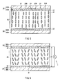
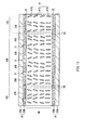
- FIG. 1 illustrates a schematic partial cross sectional view of liquid crystal display units (or liquid crystal display devices) according to a first aspect to a third aspect of the present invention.
- the liquid crystal display unit has a plurality of pixels 10 (10A, 10B, 10C and the like).
- a liquid crystal layer 40 containing a liquid crystal molecule 41 is provided between a TFT (Thin Film Transistor) substrate 20 and a CF (Color Filter) substrate 30 with alignment films 22 and 32 in between.
- the liquid crystal display unit (liquid crystal display device) is a so-called transmissive liquid crystal display unit, and the display mode thereof is vertical alignment (VA) mode.
- FIG. 1 illustrates non-driving state in which a drive voltage is not applied.
- a plurality of pixel electrodes 20B are arranged, for example, in a state of matrix on the surface on the side opposed to the CF substrate 30 of a glass substrate 20A.
- a TFT switching device including a gate, a source, a drain and the like that respectively drive the plurality of pixel electrodes 20B and a gate line, a source line and the like (not illustrated) connected to the TFT switching device are provided thereon.
- the pixel electrode 20B is provided for every pixel that is electrically separated by a pixel separating section 50 on the glass substrate 20A.
- the pixel electrode 20B is made of a material having transparency such as ITO (indium tin oxide).
- the pixel electrode 20B is provided with a slit section 21 (section where the electrode is not formed) having a stripe-like or V-shaped pattern in each pixel.
- a slit section 21 section where the electrode is not formed
- the slit section 21 is an alignment regulation section for regulating alignment of the entire liquid crystal molecules 41 in the liquid crystal layer 40 in order to secure favorable display characteristics.
- alignment direction of the liquid crystal molecule 41 in the case where a drive voltage is applied is regulated by the slit section 21.
- direction angle of the liquid crystal molecules in the case where pretilt is given is determined by electric field direction, and the electric field direction is determined by the alignment regulation section.
- a color filter (not illustrated) composed of, for example, red (R), green (G), and blue (B) stripe-like filters and an opposed electrode 30B are arranged over the almost whole area of an effective display region on the face opposed to the TFT substrate 20 of the glass substrate 30A.
- the opposed electrode 30B is made of a material having transparency such as ITO.
- the alignment film 22 is provided on the surface on the liquid crystal layer 40 side of the TFT substrate 20 to cover the pixel electrode 20B and the slit section 21.
- the alignment film 32 is provided on the surface on the liquid crystal layer 40 side of the CF substrate 30 to cover the opposed electrode 30B.
- the alignment films 22 and 32 regulate alignment of the liquid crystal molecules 41.
- the alignment films 22 and 32 have a function to align the liquid crystal molecules 41 in the direction vertical to the substrate face and to give pretilt to the liquid crystal molecules 41 (41A and 41B) in the vicinity of the substrate.
- a slit section is not provided on the side of the CF substrate 30.
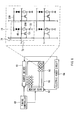
- FIG. 8 illustrates a circuit structure of the liquid crystal display unit illustrated in FIG. 1 .
- the liquid crystal display unit includes a liquid crystal display device having the plurality of pixels 10 provided in a display region 60.
- a source driver 61 In the liquid crystal display unit, around the display region 60, a source driver 61, a gate driver 62, a timing controller 63 for controlling the source driver 61 and the gate driver 62, and an electric power circuit 64 for supplying electric power to the source driver 61 and the gate driver 62 are provided.
- the display region 60 is a region where a picture is displayed, and is a region where a picture is able to be displayed by arranging the plurality of pixels 10 in a state of matrix.
- FIG. 8 illustrates the display region 60 including the plurality of pixels 10, and separately illustrates an enlarged region corresponding to four pixels 10.
- a plurality of source lines 71 are arranged in rows, and a plurality of gate lines 72 are arranged in columns, and the pixel 10 is arranged in an intersection of the source line 71 and the gate line 72.
- the respective pixels 10 include a transistor 121 and a capacitor 122 together with the pixel electrode 20B and the liquid crystal layer 40.
- the source electrode is connected to the source line 71
- the gate electrode is connected to the gate line 72
- the drain electrode is connected to the capacitor 122 and the pixel electrode 20B.
- the respective source lines 71 are connected to the source driver 61, and an image signal is supplied from the source drive 61.
- the respective gate lines 72 are connected to the gate driver 62, and a scanning signal is sequentially supplied from the gate driver 62.
- the source driver 61 and the gate driver 62 select a specific pixel 10 out of the plurality of pixels 10.
- the timing controller 63 outputs, for example, an image signal (for example, respective RGB picture signals corresponding to red, green, and blue) and a source driver control signal for controlling operation of the source driver 61 to the source driver 61. Further, the timing controller 63 outputs, for example, a gate driver control signal for controlling operation of the gate driver 62 to the gate driver 62.
- Examples of the source driver control signal include a horizontal synchronization signal, a start pulse signal, a clock signal for the source driver and the like.
- Examples of the gate driver control signal include a vertical synchronization signal and a clock signal for the gate driver and the like.
- a drive voltage is applied between the pixel electrode 20B and the opposed electrode 30B by the following procedure and thereby a picture is displayed.
- the source driver 61 individually supplies an image signal to a given source line 71 based on an image signal inputted similarly from the timing controller 63.
- the gate driver 62 sequentially supplies a scanning signal to the gate line 72 at a given timing. Thereby, the pixel 10 located in the intersection of the source line 71 supplied with the image signal and the gate line 72 supplied with the scanning signal is selected, and a drive voltage is applied to the pixel 10.
- a first embodiment relates to the VA mode liquid crystal display unit (or liquid crystal display device) according to the first aspect of the present invention, and methods of manufacturing a liquid crystal display units (or liquid crystal display devices) according to the first aspect of the present invention and the third aspect of the present invention.
- the alignment films 22 and 32 contain one or more polymer compounds having a cross-linking structure in a side chain (compound after alignment process). Liquid crystal molecules are given with pretilt by the cross-linked compound.
- the compound after alignment process is generated by forming the alignment films 22 and 32 containing one or more polymer compounds (compound before alignment process) having a main chain and a side chain, providing the liquid crystal layer 40, and then bridging the polymer compound; or radiating energy line to the polymer compound; or more specifically, by reacting a crosslinkable functional group contained in the side chain while applying electric field or magnetic field.
- the compound after alignment process contains a structure in which the liquid crystal molecules are arranged in a given direction (specifically diagonal direction) to the pair of substrates (specifically, the TFT substrate 20 and the CF substrate 30).
- the compound after alignment process is contained in the alignment films 22 and 32.
- the liquid crystal molecules 41 in the vicinity of the alignment films 22 and 32 are able to be given with pretilt. Accordingly, the response rate becomes increased, and the display characteristics are improved.
- the compound before alignment process preferably contains a structure with high heat resistivity as a main chain.
- the compound after alignment process in the alignment films 22 and 32 retains alignment regulation ability for the liquid crystal molecules 41.
- response characteristics and display characteristics such as contrast are favorably retained, and reliability is secured.
- the main chain preferably contains imide bond in a repeat unit.
- Examples of compounds before alignment process containing imide bond in the main chain include a polymer compound containing a polyimide structure expressed by Formula (3).
- the polymer compound containing the polyimide structure shown in Formula (3) may be composed of one of the polyimide structures shown in Formula (3), may contain various types of the polyimide structures that are randomly linked, or may contain other structure in addition to the structure shown in Formula (3).
- R1 represents a tetravalent organic group
- R2 represents a bivalent organic group
- n1 represents an integer number of 1 or more.
- R1 and R2 in Formula (3) are arbitrary as long as R1 and R2 are a tetravalent or bivalent group containing carbon.
- One of R1 and R2 preferably contains a crosslinkable functional group as a side chain. Thereby, in the compound after alignment process, sufficient alignment regulation ability is easily obtained.
- a plurality of side chains are bonded to a main chain. It is enough that at least one of the plurality of side chains contains a crosslinkable functional group. That is, the compound before alignment process may contain a side chain not showing crosslinkable characteristics in addition to the side chain having crosslinkable characteristics.
- the number of types of the side chains containing a crosslinkable functional group may be one or plural number.
- the crosslinkable functional group is arbitrary as long as the crosslinkable functional group is a functional group that is crosslinkable after the liquid crystal layer 40 is formed.
- the crosslinkable functional group may be a group that forms a cross-linking structure by photoreaction, or may be a group that forms a cross-linking structure by heat reaction.
- a photoreactive crosslinkable functional group (photosensitive group having photosensitivity) that forms a cross-linking structure by photoreaction is preferable, since thereby the liquid crystal display unit (liquid crystal display device) in which alignment of the liquid crystal molecule 41 is easily regulated in a given direction, response characteristics are improved, and favorable display characteristics are shown is able to be easily manufactured.
- Examples of the photoreactive crosslinkable functional group include a group containing one structure of chalcone, cinnamate, cinnamoyl, coumarin, maleimide, benzophenone, norbornene, orizanol, and chitosan.
- examples of group containing the structure of chalcone, cinnamate, or cinnamoyl include a group expressed by Formula (41). In the case where a compound before alignment process having a side chain containing the group shown in Formula (41) is cross-linked, for example, a structure shown in Formula (42) is formed.
- the compound after alignment process generated from the polymer compound containing the group shown in Formula (41) contains the structure shown in Formula (42) having cyclobutane skeleton.
- the photoreactive crosslinkable functional group such as maleimide shows polymerization reaction in addition to photodimerization reaction.
- crosslinkable functional group includes not only a crosslinkable functional group showing photodimerization reaction but also a crosslinkable functional group showing polymerization reaction.
- concept of "cross-link” includes not only photodimerization reaction but also polymerization reaction.
- R3 represents a bivalent group containing an aromatic ring
- R4 represents a monovalent group containing 1 or more ring structures
- R5 represents a hydrogen atom, an alkyl group, or a derivative thereof.
- R3 in Formula (41) is arbitrary as long as R3 is a bivalent group containing an aromatic ring such as benzene ring, which may contain a carbonyl group, ether bond, ester bond, or a hydrocarbon group in addition to the aromatic ring.
- R4 in Formula (41) is arbitrary as long as R4 is a monovalent group containing 1 or more ring structures, which may contain a carbonyl group, ether bond, ester bond, a hydrocarbon group, a halogen atom or the like in addition to the ring structure.
- the ring structure contained in R4 is arbitrary as long as the ring contains carbon as an element composing a skeleton.
- R5 in Formula (41) is arbitrary as long as R5 is a hydrogen atom, an alkyl group, or a derivative thereof.
- “derivative” means a group obtained by substituting a substitution group such as a halogen atom for part or all of hydrogen atoms contained in the alkyl group.
- the carbon number of the alkyl group introduced as R5 is arbitrary.
- R5 a hydrogen atom or a methyl group is preferable, since thereby favorable cross-linking reactivity is obtained.
- Each R3 in Formula (42) may be identical with each other, or different from each other. The same is applied to each R4 and each R5 in Formula (41).
- Examples of R3, R4, and R5 in Formula (42) include substances similar to the foregoing R3, R4, and R5 in Formula (41).
- Examples of the group shown in Formula (41) include groups expressed by Formula (41-1) to Formula (41-27).
- the group shown in Formula (41) is not limited to the groups shown in Formula (41-1) to Formula (41-27), as long as a group has the structure shown in Formula (41).
- the compound before alignment process preferably contains a structure for aligning the liquid crystal molecules 41 in a direction vertical to the substrate face (hereinafter referred to as "vertical alignment induction structure section").
- vertical alignment induction structure section a structure for aligning the liquid crystal molecules 41 in a direction vertical to the substrate face.
- the compound before alignment process contains the polyimide structure shown in the foregoing Formula (3)
- two types of structures that are a structure containing a vertical alignment induction structure section (repeat unit) as R2 and a structure containing a crosslinkable functional group (repeat unit) as R2 are preferably contained, since it is easily available.
- the vertical alignment induction structure section is contained in the compound before alignment process
- the vertical alignment induction structure section is also contained in the compound after alignment process.
- Examples of the vertical alignment induction structure section include an alkyl group with the carbon number of 10 or more, a halogenated alkyl group with the carbon number of 10 or more, an alkoxy group with the carbon number of 10 or more, a halogenated alkoxy group with the carbon number of 10 or more, and an organic group containing a ring structure.
- Specific examples include structures expressed by Formula (5-1) to Formula (5-6) as a structure containing a vertical alignment induction structure section.
- Y1 represents an alkyl group with the carbon number of 10 or more, an alkoxy group with the carbon number of 10 or more, or a monovalent organic group containing a ring structure.
- Y2 to Y15 represent a hydrogen atom, an alkyl group with the carbon number of 10 or more, an alkoxy group with the carbon number of 10 or more, or a monovalent organic group containing a ring structure.
- At least one of Y2 and Y3, at least one of Y4 to Y6, at least one of Y7 and Y8, at least one of Y9 to Y12, and at least one of Y13 to Y15 are an alkyl group with the carbon number of 10 or more, an alkoxy group with the carbon number of 10 or more, or a monovalent organic group containing a ring structure.
- Y11 and Y12 may be bonded to each other to form a ring structure.
- Examples of the monovalent organic group containing a ring structure as a vertical alignment induction structure section include groups expressed by Formula (6-1) to Formula (6-23). Further, examples of the bivalent organic group containing a ring structure as a vertical alignment induction structure section include groups expressed by Formula (7-1) to Formula (7-7).
- al to a3 represent an integer number from 0 to 21 both inclusive.
- a1 represents an integer number from 0 to 21 both inclusive.
- the vertical alignment induction structure section is not limited to the foregoing groups as long as a structure functioning to align the liquid crystal molecules 41 in the direction vertical to the substrate face is contained.
- the polymer compound before cross-link is composed of a compound having a group expressed by Formula (1) as a side chain in addition to a crosslinkable functional group.
- the group shown in Formula (1) is able to move along the liquid crystal molecules 41, and thus in bridging the compound before alignment process, the group shown in Formula (1) is fixed together with the crosslinkable functional group in a state that the group shown in Formula (1) is located along the alignment direction of the liquid crystal molecules 41. Due to the fixed group shown in Formula (1), the alignment direction of the liquid crystal molecules 41 is able to be more easily regulated in a given direction. Therefore, manufacturing the liquid crystal display device having favorable display characteristics is able to be more facilitated.
- R1 represents a straight chain or branched chain bivalent organic group with the carbon number of 3 or more, and is bonded to a main chain of the polymer compound before cross-link (compound before alignment process).
- R2 represents a bivalent organic group containing a plurality of ring structures, and one of atoms composing the ring structures is bonded to R1.
- R3 represents a hydrogen atom, a halogen atom, an alkyl group, an alkoxy group, and a monovalent group having a carbonate group, or a derivative thereof.
- R1 in Formula (1) is a region functioning as a spacer section to fix R2 and R3 on the main chain and to make R2 and R3 easily and freely move along the liquid crystal molecules 41.
- R1 include an alkylene group and the like.
- the alkylene group may have ether bond between each intermediate carbon atom.
- the number of places having the ether bond may be one or more.
- R1 may have a carbonyl group or a carbonate group.
- the carbon number of R1 is more preferably 6 or more.
- the carbon number is preferably determined so that the length of R1 becomes approximately equal to the length of the end chain of the liquid crystal molecules 41.
- R2 in Formula (1) is a section along a ring structure (core region) contained in a general nematic liquid crystal molecule.
- R2 include a group or a skeleton similar to a ring structure contained in a liquid crystal molecule such as an 1,4-phenylene group, an 1,4-cyclohexylene group, a pyrimidine-2,5-diyl group, an 1,6-naphthalene group, and a bivalent group having a steroid skeleton or a derivative thereof.
- “derivative” means a group obtained by introducing one or more substitution groups into the foregoing series of groups.
- R3 in Formula (1) is a section along the end chain of a liquid crystal molecule.
- examples of R3 include an alkylene group and an alkylene halide group.
- the alkylene group or the alkylene halide group may have ether bond between each intermediate carbon atom.
- the number of places having the ether bond may be one or more.
- R3 may have a carbonyl group or a carbonate group. The carbon number of R3 is more preferably 6 or more for a reason similar to that of R1.
- Specific examples include a monovalent group expressed by Formula (1-1) to Formula (1-8) as the group shown in Formula (1).
- the group shown in Formula (1) is not limited to the foregoing groups, as long as a group is able to move along the liquid crystal molecules 41.
- the polymer compound before cross-link (compound before alignment process) is composed of a compound having a group expressed by Formula (2) as a side chain.
- a region along the liquid crystal molecules 41 and a freely movable region are contained in addition to a crosslinkable region, fixation is enabled in a state that the region of the side chain is located more along the liquid crystal molecules 41.
- the alignment of the liquid crystal molecules 41 is able to be more easily regulated in a given direction. Therefore, manufacturing the liquid crystal display device having favorable display characteristics is able to be more facilitated.
- R11 represents a straight chain or branched chain bivalent organic group with the carbon number of 1 to 20 both inclusive or preferably 3 to 12 both inclusive that may contain an ether group or an ester group, and is bonded to a main chain of a polymer compound or a cross-linked compound (compound before alignment process or compound after alignment process). Otherwise, R11 represents an ether group or an ester group, and is bonded to a main chain of a polymer compound or a cross-linked compound (compound before alignment process or compound after alignment process).
- R12 represents a bivalent group containing one structure of chalcone, cinnamate, cinnamoyl, coumarin, maleimide, benzophenone, norbornene, orizanol, and chitosan, or an ethynylene group.
- R 13 represents a bivalent organic group containing a plurality of ring structures.
- R14 represents a hydrogen atom, a halogen atom, an alkyl group, an alkoxy group, and a monovalent group having a carbonate group, or a derivative thereof.
- R11 in Formula (2) is a region capable of freely moving in the compound before alignment process, and preferably has flexibility in the compound before alignment process.
- R11 include the group described for R1 in Formula (1).
- R12 to R14 are easily moved centering on R11 as an axis, and thus R13 and R14 are easily located along the liquid crystal molecules 41.
- the carbon number of R11 is more preferably from 6 to 10 both inclusive.
- R12 in Formula (2) is a region having a crosslinkable functional group.
- the crosslinkable functional group may be a group that forms a cross-linking structure by photoreaction, or may be a group that forms a cross-linking structure by heat reaction.
- Specific examples of R12 include a bivalent group containing one structure of chalcone, cinnamate, cinnamoyl, coumarin, maleimide, benzophenone, norbornene, orizanol, and chitosan, or an ethynylene group.
- R13 in Formula (2) is a region capable of being located along the core region of the liquid crystal molecule 41.
- Examples of R13 include the groups described for R2 in Formula (1).
- R14 in Formula (2) is a region being located along the end chain of the liquid crystal molecule 41.
- Examples of R14 include the groups described for R3 in Formula (1).
- Specific examples of the group shown in Formula (2) include monovalent groups expressed by Formula (2-1) to Formula (2-7).
- n represents an integer number from 3 to 20 both inclusive.
- the compound (compound after alignment process) obtained by bridging the polymer compound (compound before alignment process) is composed of a side chain and a main chain supporting the side chain to the substrate.
- the side chain is bonded to the main chain, and is composed of a cross-linked section in which part of the side chain is cross-linked and an end structure section bonded to the cross-linked section.
- the liquid crystal molecule is located along the end structure section or is sandwiched by the end structure sections, the liquid crystal molecule is given with pretilt.
- the compound (compound after alignment process) obtained by deforming the polymer compound (compound before alignment process) is composed of a side chain and a main chain supporting the side chain to the substrate.
- the side chain is bonded to the main chain, and is composed of a deformed section in which part of the side chain is deformed and an end structure section bonded to the deformed section.
- the liquid crystal molecule is located along the end structure section or is sandwiched by the end structure sections, the liquid crystal molecule is given with pretilt.
- the compound obtained by radiating energy line to the polymer compound is composed of a side chain and a main chain supporting the side chain to the substrate.
- the side chain is bonded to the main chain, and is composed of a cross-linked/deformed section in which part of the side chain is cross-linked or deformed and an end structure section bonded to the cross-linked/deformed section.
- the liquid crystal molecule is located along the end structure section or is sandwiched by the end structure sections, the liquid crystal molecule is given with pretilt.
- the cross-linked section in which part of the side chain is cross-linked corresponds to R12 (after cross-link) in Formula (2).
- the end structure section corresponds to R13 and R14 in Formula (2).
- the crosslinkable sections in two side chains extending from the main chain are cross-linked, part of the liquid crystal molecule is sandwiched between the end structure section extending from one cross-linked section and the end structure section extending from the other cross-linked section, and the end structure section is fixed in a state that a given angle exists between the end structure section and the substrate.
- the liquid crystal molecule is given with pretilt.
- Such a state is illustrated in the conceptual diagram of FIG. 15 .
- the compound (compound after alignment process) obtained by bridging the polymer compound (compound before alignment process) is composed of a side chain and a main chain supporting the side chain to the substrate.
- the side chain is bonded to the main chain, and is composed of a cross-linked section in which part of the side chain is cross-linked and an end structure section that is bonded to the cross-linked section and has a mesogenic group.
- the side chain may have a photodimerization photosensitive group.
- the main chain may be bonded to the bride section by covalent bond, and the cross-linked section may be bonded to the end structure section by covalent bond.
- the compound (compound after alignment process) obtained by deforming the polymer compound (compound before alignment process) is composed of side chain and a main chain supporting the side chain to the substrate.
- the side chain is bonded to the main chain, and is composed of a deformed section in which part of the side chain is deformed and an end structure section that is bonded to the deformed section and has a mesogenic group.
- the compound (compound after alignment process) obtained by radiating energy line to the polymer compound (compound before alignment process) is composed of a side chain and a main chain supporting the side chain to the substrate.
- the side chain is bonded to the main chain, and is composed of a cross-linked/deformed section in which part of the side chain is cross-linked or deformed, and an end structure section that is bonded to the cross-linked/deformed section and has a mesogenic group.
- examples of the photodimerization photosensitive group as a crosslinkable functional group include, as described above, a group containing one structure of chalcone, cinnamate, cinnamoyl, coumarin, maleimide, benzophenone, norbornene, orizanol, and chitosan. Further, it is possible that an adamant mesogenic group composing an end structure section expresses liquid crystal characteristics as a side chain or does not express liquid crystal characteristics. Specific examples of the structure include a steroid derivative, a cholesterol derivative, biphenyl, triphenyl, and naphthalene and the like. Further, examples of the end structure section include R13 and R14 in Formula (2).
- the surface roughness Ra of a first alignment film is 1 nm or less.
- the compound after alignment process may contain an unreacted crosslinkable functional group. However, if reaction is initiated during drive, alignment of the liquid crystal molecules 41 may be disturbed. Thus, the portion of the unreacted crosslinkable functional group is preferably small. Whether or not the compound after alignment process contains the unreacted crosslinkable functional group is able to be checked by disassembling the liquid crystal display unit and analyzing the alignment films 22 and 32 by a transmissive type or reflection type FT-IR (Fourier transform infrared spectrophotometer). Specifically, first, the liquid crystal display unit is disassembled, and the surface of the alignment films 22 and 32 is washed with an organic solvent or the like. After that, the alignment films 22 and 32 are analyzed by FT-IR.
- FT-IR Fast Fourier transform infrared spectrophotometer
- the alignment films 22 and 32 may contain other vertical aligner in addition to the foregoing polymer compound after alignment process.
- other vertical aligner include polyimide having a vertical alignment induction structure section and polysiloxane having a vertical alignment induction structure section and the like.
- the liquid crystal layer 40 contains the liquid crystal molecules 41 having negative dielectric constant anisotropy.
- the liquid crystal molecules 41 have a rotationally-symmetrical shape centering on the long axis and the short axis that are perpendicular to each other, and have negative dielectric constant anisotropy.
- the liquid crystal molecule 41 is able to be categorized into a liquid crystal molecule 41A retained by the alignment film 22 in the vicinity of the interface with the alignment film 22, a liquid crystal molecule 41B retained by the alignment film 32 in the vicinity of the interface with the alignment film 32, and a liquid crystal molecule 41C other than the liquid crystal molecule 41A and the liquid crystal molecule 41B.
- the liquid crystal molecule 41C is located in the intermediate region in the thickness direction of the liquid crystal layer 40, and is aligned so that the long axis direction (director) of the liquid crystal molecule 41C becomes almost vertical to glass substrates 20A and 30A in a state that a drive voltage is off.
- the liquid crystal molecule 41C is aligned at a tilt so that the director of the liquid crystal molecule 41C becomes in parallel with the glass substrates 20A and 30A.
- Such behavior results from a fact that in the liquid crystal molecule 41C, the dielectric constant in the long axis direction is smaller than that in the short axis direction.
- the liquid crystal molecule 41A and the liquid crystal molecule 41B have similar characteristics, and thus the liquid crystal molecule 41A and the liquid crystal molecule 41B fundamentally show behavior similar to that of the liquid crystal molecule 41C according to on/off state change of the drive voltage.
- the liquid crystal molecule 41A is given with pretilt ⁇ 1 by the alignment film 22, and the director thereof is tilted from the normal line direction of the glass substrates 20A and 30A.
- the liquid crystal molecule 41B is given with pretilt ⁇ 2 by the alignment film 32, and the director thereof is tilted from the normal line direction of the glass substrates 20A and 30A.
- "to be retained” means that the orientation films 22 and 32 are not firmly fixed with the liquid crystal molecules 41A and 41C, and alignment of the liquid crystal molecules 41 is regulated.
- pretilt ⁇ ( ⁇ 1 and ⁇ 2) means a tilt angle of a director D of the liquid crystal molecule 41 (41A and 41B) in the Z direction in a state that a drive voltage is off, where the direction vertical to the surface of the glass substrates 20A and 30A (normal line direction) is Z as illustrated in FIG. 2 .
- both the pretilt ⁇ 1 and the pretilt ⁇ 2 have a value larger than 0 deg.
- the pretilt ⁇ 1 and the pretilt ⁇ 2 are preferably different from each other. Thereby, response rate to application of a drive voltage is more improved than in a case that both the pretilt ⁇ 1 and the pretilt ⁇ 2 are 0 deg.
- the larger pretilt ⁇ out of the pretilt ⁇ 1 and the pretilt ⁇ 2 is more desirably from 1 deg to 4 deg both inclusive.
- FIG. 5 illustrates a cross section for one pixel for simplicity.
- the alignment film 22 is formed on the surface of the TFT substrate 20, and the alignment film 32 is formed on the surface of the CF substrate 30 (step S101).
- the TFT substrate 20 is formed by providing the pixel electrode 20B having a given slit section 21 in a state of, for example, matrix on the surface of the glass substrate 20A. Further, the CF substrate 30 is formed by providing the opposed electrode 30B on the color filter of the glass substrate 30A on which the color filter is formed.
- the compound before alignment process or a polymer compound precursor as the compound before alignment process, a solvent, and if necessary a vertical aligner are mixed, and thereby a liquid alignment film material is prepared.
- Examples of the polymer compound precursor as the compound before alignment process include polyamic acid having a crosslinkable functional group in the case where the polymer compound having a crosslinkable functional group as a side chain contains the polyimide structure shown in Formula (3).
- the polyamic acid as the polymer compound precursor is synthesized, for example, by reacting a diamine compound with a tetracarboxylic acid dianhydride. At least one of the diamine compound and the tetracarboxylic acid dianhydride herein used has a crosslinkable functional group.
- Examples of the diamine compound include a compound having a crosslinkable functional group expressed by Formula (A-1) to Formula (A-15).
- Examples of the tetracarboxylic acid dianhydride include a compound having a crosslinkable functional group expressed by Formula (a-1) to Formula (a-10).
- the compound expressed by Formula (A-9) to Formula (A-15) is a compound structuring the cross-linked section and the end structure section of the cross-linked polymer compound in the 1C structure of the present invention.
- examples of the compound structuring the cross-linked section and the end structure section of the cross-linked polymer compound in the 1C structure of the present invention include a compound expressed by Formula (F-1) to Formula (F-18).
- pretilt may be given to the liquid crystal molecule along the end structure section of the compound expressed by Formula (F-1) to Formula (F-3), Formula (F-7) to Formula (F-9), and Formula (F-13) to Formula (F-15), while pretilt may be given to the liquid crystal molecule sandwiched by the end structure sections of the compound expressed by Formula (F-4) to Formula (F-6), Formula (F-10) to Formula (F-12), and Formula (F-16) to Formula (F-18).
- X1 to X4 represent a single bond or a bivalent organic group.
- X5 to X7 represent a single bond or a bivalent organic group.
- compounds having a vertical alignment induction structure section expressed by Formula (B-1) to Formula (B-36) as a diamine compound or compounds having a vertical alignment induction structure section expressed by Formula (b-1) to Formula (b-3) as tetracarboxylic acid dianhydride may be used.
- a4 to a6 represent an integer number from 0 to 21 both inclusive.
- a4 represents an integer number from 0 to 21 both inclusive.
- a4 represents an integer number from 0 to 21 both inclusive.
- compound precursor is the group shown in on to the foregoing a group capable of la (C-1) to Formula
- a compound having a group capable of being located along the liquid crystal molecule 41 expressed by Formula (D-1) to Formula (D-7) as a diamine compound may be used.
- n represents an integer number from 3 to 20 both inclusive.
- the polyamic acid as the polymer compound precursor is synthesized so that the compound before alignment process contains two types of structures that are a structure containing a vertical alignment induction structure section and a structure containing a crosslinkable functional group as R2 in formula (3)
- a diamine compound and a tetracarboxylic acid dianhydride are selected as follows.
- At least one of the compounds having a crosslinkable functional group expressed by Formula (A-1) to Formula (A-15), at least one of the compounds having a vertical alignment induction structure section expressed by Formula (B-1) to Formula (B-36) and Formula (b-1) to Formula (b-3), and at least one of the tetracarboxylic acid dianhydrides expressed by Formula (E-1) to Formula (E-28) are used.
- R1 and R2 in Formula (E-23) are the same or a different alkyl group, alkoxy group, or halogen atom.
- the halogen atom type is arbitrary.
- R1 and R2 are an alkyl group, an alkoxy group, or a halogen atom.
- a diamine compound and a tetracarboxylic acid dianhydride are selected as follows. That is, at least one of the compounds having a crosslinkable functional group shown in Formula (A-1) to Formula (A-15), at least one of the compounds shown in Formula (C-1) to Formula (C-20), and at least one of the tetracarboxylic acid dianhydride shown in Formula (E-1) to Formula (E-28) are used.
- a diamine compound and a tetracarboxylic acid dianhydride are selected as follows. That is, at least one of the compounds having a crosslinkable functional group shown in Formula (A-1) to Formula (A-15), at least one of the compounds shown in Formula (D-1) to Formula (D-7), and at least one of the tetracarboxylic acid dianhydride shown in Formula (E-1) to Formula (E-28) are used.
- the content of the compound before alignment process or the polymer compound precursor as the compound before alignment process in the alignment film material is preferably from 1 wt% to 30 wt% both inclusive, and more preferably from 3 wt% to 10 wt% both inclusive. Further, the alignment film material may be mixed with a photopolymerization initiator or the like according to needs.
- the TFT substrate 20 and the CF substrate 30 are respectively coated or printed with the prepared alignment film material so that the pixel electrode 20B, the slit section 21, and the opposed electrode 30B are covered therewith, and then heat treatment is provided.
- Heat treatment temperature is preferably 80 deg C or more, and more preferably from 150 deg C to 200 deg C both inclusive. Further, in the heat treatment, heating temperature may be changed in stages. Thereby, the solvent contained in the coated or printed alignment film material is evaporated, and the alignment films 22 and 32 containing the polymer compound (compound before alignment process) having a crosslinkable functional group as a side chain are formed. After that, rubbing or the like may be provided according to needs.
- the compound before alignment process in the alignment films 22 and 32 may be in the state illustrated in FIG. 4 . That is, the compound before alignment process contains main chains Mc (Mc1 to Mc3) and crosslinkable functional groups A introduced as a side chain into the main chains Mc. The main chains Mc 1 to Mc3 are not linked. The crosslinkable functional groups A in this state are oriented randomly by thermal motion.
- the TFT substrate 20 and the CF substrate 30 are arranged so that the alignment film 22 and the alignment film 32 are opposed to each other, and the liquid crystal layer 40 containing the liquid crystal molecules 41 is sealed between the alignment film 22 and the alignment film 32 (step S102).
- a spacer projection for securing a cell gap such as plastic beads is dispersed toward one of the faces on which the alignment films 22 and 32 are formed of the TFT substrate 20 and the CF substrate 30, and a seal section is printed by using an epoxy adhesive or the like by screen print process.
- the TFT substrate 20 and the CF substrate 30 are bonded to the spacer projection and the seal section in between so that the alignment films 22 and 32 are opposed to each other, and a liquid crystal material containing the liquid crystal molecules 41 is injected.
- the seal section is cured by heating or the like, and thereby the liquid crystal material is sealed between the TFT substrate 20 and the CF substrate 30.
- FIG. 5 illustrates a cross sectional structure of the liquid crystal layer 40 sealed between the alignment films 22 and 32.
- a voltage V 1 is applied between the pixel electrode 20B and the opposed electrode 30B by using a voltage application means 1 (step S103).
- the voltage V1 is, for example, from 5 volt to 30 volt both inclusive.
- electric field electric voltage
- the orientation angle (deviation angle) of the liquid crystal molecules 41 is determined by the direction of the electric field
- the polar angle (zenith angle) is determined by electric field intensity.
- the tilt angle of the liquid crystal molecules 41 is approximately equal to the pretilt ⁇ 1 that is given to the liquid crystal molecule 41A retained in the alignment film 22 in the vicinity of the interface with the alignment film 22and the pretilt ⁇ 2 that is given to the liquid crystal molecule 41B retained in the alignment film 32 in the vicinity of the interface with the alignment film 32 in the after-mentioned step.
- the values of the pretilt ⁇ 1 and the pretilt ⁇ 2 of the liquid crystal molecules 41A and 41B are able to be controlled.
- energy line specifically, ultraviolet UV
- ultraviolet UV ultraviolet
- the alignment films 22 and 32 for example, from the outside of the TFT substrate 20. That is, ultraviolet is irradiated to the liquid crystal layer while electric field or magnetic field is applied so that the liquid crystal molecules 41 are aligned in a direction diagonal to the surface of the pair of substrates 20 and 30.
- the crosslinkable functional group contained in the compound before alignment process in the alignment films 22 and 32 is reacted, and the compound before alignment process is cross-linked (step S104).
- a legitimate response direction of the liquid crystal molecules 41 is stored by the compound after alignment process, and pretilt is given to the liquid crystal molecules 41 in the vicinity of the alignment films 22 and 32.
- the polymer after alignment process is formed in the alignment films 22 and 32.
- the pretilt ⁇ 1 and the pretilt ⁇ 2 are given to the liquid crystal molecules 41A and 41B located in the vicinity of the interface with the alignment films 22 and 32 in the liquid crystal layer 40 in a non-driving state.
- ultraviolet UV ultraviolet containing a large amount of optic element with a wavelength of about 365 nm is preferable.
- ultraviolet UV is irradiated from the outside of the TFT substrate 20.
- ultraviolet UV may be irradiated from the outside of the CF substrate 30, or ultraviolet UV may be irradiated from the outside of both the TFT substrate 20 and the CF substrate 30.
- ultraviolet UV is preferably irradiated from the substrate side with higher transmittance.
- ultraviolet UV is irradiated from the outside of the CF substrate 30
- the ultraviolet UV is absorbed by the color filter and cross-linking reaction is hardly generated depending on the wavelength range of the ultraviolet UV.
- ultraviolet UV is preferably irradiated from outside of the TFT substrate 20 (substrate side having the pixel electrode).
- the compound after alignment process in the alignment films 22 and 32 is in the state illustrated in FIG. 7(B) . That is, the direction of the crosslinkable functional groups A introduced into the main chains Mc of the compound before alignment process is changed according to the alignment direction of the liquid crystal molecules 41, the crosslinkable functional groups A that are physically close to each other are reacted with each other, and accordingly a connection section Cr is formed. Due to the compound after alignment process generated as above, the alignment films 22 and 32 give the pretilt ⁇ 1 and the pretilt ⁇ 2 to the liquid crystal molecules 41A and 41B.
- the connection section Cr may be formed among the compound before alignment process, or may be formed in the compound before alignment process. That is, as illustrated in FIG.
- connection section Cr may be formed between the crosslinkable functional group A of the compound before alignment process having the main chain Mc1 and the crosslinkable functional group A of the compound before alignment process having the main chain Mc2. Further, the connection section Cr may be formed by reacting the crosslinkable functional groups A introduced into the same main chain Mc3 as in the polymer compound having the main chain Mc3.
- the liquid crystal display unit (liquid crystal display device) illustrated in FIG. 1 was able to be completed.
- liquid crystal display unit in the selected pixel 10, in the case where a drive voltage is applied, alignment state of the liquid crystal molecules 41 included in the liquid crystal layer 40 is changed according to the potential difference between the pixel electrode 20B and the opposed electrode 30B.
- the liquid crystal molecules 41A and 41B located in the vicinity of the alignment films 22 and 32 fall over in its direction, and such operation is transmitted to the other liquid crystal molecules 41C.
- the liquid crystal molecules 41 respond to take a stance to be approximately horizontal (parallel) to the TFT substrate 20 and the CF substrate 30.
- optical characteristics of the liquid crystal layer 40 are changed, incident light to the liquid crystal display device becomes modulated output light, gradation sequence is expressed based on the output light, and thereby an image is displayed.
- liquid crystal display device not given with pretilt process and a liquid crystal display unit including the same, even if an alignment regulation section such as a slit section for regulating alignment of liquid crystal molecules is provided on a substrate, in the case where a drive voltage is applied, the liquid crystal molecules aligned in the direction vertical to the substrate falls so that the director thereof is oriented in a given direction in the in-plane direction of the substrate.
- the orientation of the director of each liquid crystal molecule varies, and the entire alignment is disarrayed. Thereby, the response rate is decreased, and the response characteristics are deteriorated. In the result, there is a problem that the display characteristics are deteriorated.
- the luminance is subsequently decreased, and reaches the luminance in a state of display again. That is, there is a problem as follows. If overdriving is performed, apparent response rate becomes faster than that of a case in which overdriving is not performed, but sufficient display quality is hardly obtained. Such a problem is hardly generated in IPS mode or FFS mode liquid crystal display devices, and may be a problem unique to the VA mode liquid crystal display device.
- the foregoing alignment films 22 and 32 give the pretilt ⁇ 1 and the pretilt ⁇ 2 to the liquid crystal molecules 41A and 41B.
- the problem initiated in the case where pretilt process is never provided is hardly generated, the response rate to a drive voltage is largely improved, and the display quality in overdriving is improved.
- the TFT substrate 20 and the CF substrate 30 is provided with the slit section 21 or the like as an alignment regulation section for regulating alignment of the liquid crystal molecules 41, display characteristics such as view angle characteristics are secured. Accordingly, the response characteristics are improved in a state that favorable display characteristics are retained.
- an alignment film is formed by radiating linear polarized light or light in a direction diagonal to the substrate face (hereinafter referred to as "diagonal light") to a precursor film containing a given polymer material provided on the substrate face, and thereby pretilt process is provided.
- a major light radiation equipment such as an equipment for radiating linear polarized light and an equipment for radiating diagonal light is necessitated in forming the alignment film.
- a more major equipment is necessitated, and the manufacturing steps become complicated.
- the alignment film is formed by using diagonal light
- a structure such as a spacer or irregularity exist on the substrate
- a region which is hidden behind the structure or the like and at which diagonal light does not arrive is generated, and desirable alignment regulation for the liquid crystal molecules is difficult in such a region.
- a crosslinkable functional group contained in the crosslinkable polymer compound in a precursor film is oriented (directed) randomly by thermal motion.
- random light non-polarized light
- the crosslinkable functional group whose reaction is initiated by radiating straight polarized light the polarized direction and the direction of the reaction region should be aligned in a given direction.
- the radiation area of diagonal light is wider than that of vertical light, the radiation amount per unit area thereof is decreased. That is, the ratio of the crosslinkable functional group responsive to linear polarized light or diagonal light is lower than that in the case where random light (non-polarized light) is irradiated in the direction vertical to the substrate face. Thus, the crosslink density (cross-linking degree) in the formed alignment film is easily decreased.
- the liquid crystal layer 40 is sealed between the alignment film 22 and the alignment film 32.
- the alignment of the liquid crystal molecules 41 becomes given alignment
- direction of the crosslinkable functional group is arrayed by the liquid crystal molecules 41 (that is, direction of the end structure section of the side chain to the substrate or the electrode is determined by the liquid crystal molecules 41)
- the compound before alignment process in the alignment films 22 and 32 is cross-linked.
- the response characteristics are able to be easily improved without using a major equipment.
- pretilt ⁇ is able to be given to the liquid crystal molecules 41 without depending on the ultraviolet radiation direction.
- a high definition pixel is able to be formed.
- the compound after alignment process is formed in a state that the direction of the crosslinkable functional groups has been already arrayed in the compound before alignment process.
- the cross-linking degree of the compound after alignment process may be higher than that of the alignment film formed by the foregoing existing manufacturing method.
- new cross-linking structures are hardly formed in driving. Therefore, the pretilt ⁇ 1 and the pretilt ⁇ 2 in the liquid crystal molecules 41A and 41B are able to be retained in a state of manufacturing, and reliability is able to be improved.
- the compound before alignment process in the alignment films 22 and 32 is cross-linked.
- the transmittance in driving the liquid crystal display device is able to be continuously increased.
- pretilt direction is disarrayed.
- order parameter as an index expressing alignment state of the liquid crystal molecules 41 is decreased.
- the partial liquid crystal molecules 41 P with the deviated pretilt direction show behavior different from that of the other liquid crystal molecules 41
- the partial liquid crystal molecules 41P are aligned in a direction different from that of the other liquid crystal molecules 41, and the transmittance becomes increased.
- the partial liquid crystal molecules 41 P are subsequently aligned in the same direction as that of the other liquid crystal molecules 41.
- director direction of the temporarily tilted liquid crystal molecules 41P becomes vertical to the substrate face
- the director direction of the liquid crystal molecules 41 P is aligned with the director direction of the other liquid crystal molecules 41. Therefore, there is a possibility that the transmittance of the liquid crystal device is not continuously increased, but is locally decreased.
- pretilt is given according to alignment direction of the liquid crystal molecules 41 by the alignment regulation section for regulating alignment of the liquid crystal molecules 41 such as the slit section 21.
- the pretilt direction of the liquid crystal molecules 41 is easily aligned, and thus the order parameter is increased (becomes close to 1).
- the liquid crystal molecules 41 show uniform behavior.
- transmittance is continuously increased.
- the alignment films 22 and 32 more easily give pretilt ⁇ .
- the response rate is able to be more improved.
- a liquid crystal display device after a liquid crystal layer is formed by using a liquid crystal material containing a monomer or the like having photopolymerization characteristics, in a state that the monomer is contained, while given alignment of the liquid crystal molecules in the liquid crystal layer is provided, light is irradiated to polymerize the monomer.
- a resultant polymer formed as above gives the liquid crystal molecules with pretilt.
- the manufactured liquid crystal display device there is a problem that an unreacted photopolymerizable monomer remains in the liquid crystal layer, and reliability is lowered. Further, to decrease the amount of the unreacted monomer, it is necessary to increase light radiation time, resulting in a problem that time (takt time) necessary for manufacture is increased.
- the alignment films 22 and 32 give the pretilt ⁇ 1 and the pretilt ⁇ 2 to the liquid crystal molecules 41A and 41B in the liquid crystal layer 40.
- reliability is able to be improved.
- takt time is able to be inhibited from being increased.
- the pretilt ⁇ is able to be favorably given to the liquid crystal molecules 41A and 41B.
- the main chain contained in the compound before alignment process is not limited to the compound containing a polyimide structure.
- the main chain may contain a polysiloxane structure, a polyacrylate structure, a polymethacrylate structure, a maleimide polymer structure, a styrene polymer structure, a styrene maleimide polymer structure, a polysaccharide structure, a polyvinyl alcohol structure or the like.
- a compound before alignment process having a main chain containing a polysiloxane structure is preferable.
- glass transition temperature Tg of the compound structuring a main chain is desirably 200 deg C or more, since thereby effect similar to that of the polymer compound containing the foregoing polyimide structure is able to be obtained.
- the compound before alignment process having a main chain mainly containing a polysiloxane structure include the polymer compound containing a polysilane structure shown in Formula (9).
- R10 and R11 in Formula (9) are arbitrary as long as R10 and R11 are a monovalent group containing carbon.
- One of R10 and R11 preferably contains a crosslinkable functional group as a side chain, since thereby sufficient alignment regulation ability is easily obtained in the compound after alignment process.
- the crosslinkable functional group in this case include the group shown in the foregoing Formula (41).
- R10 an R11 represent a monovalent organic group
- m1 represents an integer number of 1 or more.
- the slit section 21 is provided in the pixel electrode 20B, and thereby alignment division is realized to improve view angle characteristics.
- the method of improving view angle characteristics is not limited to the slit section 21 provided in the pixel electrode 20B.
- a projection as an alignment regulation section may be provided between the pixel electrode 20B and the alignment film 22. By providing such a projection, effect similar to that in the case of providing the slit section 21 is able to be obtained.
- a projection as an alignment regulation section may be also provided between the opposed electrode 30B and the alignment film 32 of the CF substrate 30. In this case, the projection on the TFT substrate 20 and the projection on the CF substrate 30 are arranged not to be opposed to each other between the substrates. In this case, effect similar to that of the foregoing case is able to be obtained.
- a second embodiment is a modified embodiment of the first embodiment.
- the description has been given of the liquid crystal display unit (liquid crystal display device) in which the alignment films 22 and 32 are formed so that the pretilt ⁇ 1 and the pretilt ⁇ 2 of the liquid crystal molecules 41A and 41B located in the vicinity of the alignment films 22 and 32 are almost the same.
- the pretilt ⁇ 1 value is different from the pretilt ⁇ 2 value.
- the TFT substrate 20 having the alignment film 22 and the CF substrate 30 having the alignment film 32 are formed in the same manner as that of the foregoing step S101.
- an ultraviolet absorber is contained in the liquid crystal layer 40 and is sealed.
- a given voltage is applied between the pixel electrode 20B and the opposed electrode 30B, ultraviolet is irradiated from the TFT substrate 20 side, and thereby the compound before alignment process in the alignment film 22 is cross-linked.
- the ultraviolet absorber is contained in the liquid crystal layer 40, the ultraviolet entering from the TFT substrate 20 side is absorbed by the ultraviolet absorber in the liquid crystal layer 40, and hardly reaches the CF substrate 30 side.
- the compound after alignment process is generated.
- a voltage different from the foregoing given voltage is applied between the pixel electrode 20B and the opposed electrode 30B, ultraviolet is irradiated from the CF substrate 30 side, and thereby the compound before alignment process in the alignment film 32 is reacted to form the compound after alignment process.
- the pretilt ⁇ 1 and the pretilt ⁇ 2 of the liquid crystal molecules 41A and 41B located in the vicinity of the alignment films 22 and 32 are able to be set.
- the pretilt ⁇ 1 value is able to be different from the pretilt ⁇ 2 value.
- the TFT substrate 20 is provided with a TFT switching device and various bus lines, and various transverse electric fields are generated in driving. Accordingly, it is desirable that the alignment film 22 on the TFT substrate 20 side is formed so that the pretilt ⁇ 1 of the liquid crystal molecules 41A located in the vicinity of the alignment film 22 is larger than the pretilt ⁇ 2 of the liquid crystal molecules 41B located in the vicinity of the alignment film 32. Thereby, alignment disarray of the liquid crystal molecules 41A caused by the transverse electric fields is able to be effectively decreased.
- a third embodiment is a modified embodiment of the first embodiment and the second embodiment.
- FIG. 10 illustrates a schematic partial cross sectional view of a liquid crystal display unit (liquid crystal display device) according to the third embodiment.
- the alignment film 22 does not contain the compound after alignment process. That is, in the third embodiment, the pretilt ⁇ 2 of the liquid crystal molecules 41B located in the vicinity of the alignment film 32 has a higher value than 0 deg, while the pretilt ⁇ 1 of the liquid crystal molecules 41A located in the vicinity of the alignment film 22 is 0 deg.
- the alignment film 22 is composed of, for example, the foregoing other vertical aligner.
- the liquid crystal display unit (liquid crystal display device) of the third embodiment is able to be manufactured by using the foregoing other vertical aligner instead of the compound before alignment process or the polymer compound precursor as the compound before alignment process in forming the alignment film 22 on the TFT substrate 20 (step S101 1 of FIG. 3 ).
- the pretilt ⁇ 1 of the liquid crystal molecules 41A is 0 deg
- the pretilt ⁇ 2 of the liquid crystal molecules 41B is larger than 0 deg.
- this liquid crystal display unit liquid crystal display device
- contrast is improved by setting the pretilt ⁇ 1 of the liquid crystal molecules 41A located on the TFT substrate 20 side to 0 deg while response rate is able to be improved by setting the pretilt ⁇ 2 of the liquid crystal molecules 41B located on the CF substrate 30 side to a larger value than 0 deg. Accordingly, the response rate to a drive voltage and the contrast are able to be improved with a proper balance.
- the alignment film 22 not containing the compound before alignment process is formed on the TFT substrate 20, and the alignment film 32 containing the compound before alignment process is formed on the CF substrate 30.
- the compound before alignment process in the alignment film 32 is reacted to synthesize the compound after alignment process.
- the alignment film 32 that gives the pretilt ⁇ to the liquid crystal molecules 41B is able to be formed without using a major light radiation equipment, and thus response characteristics are able to be improved easily.
- a photopolymerizable monomer is polymerized after the liquid crystal layer is sealed by using a liquid crystal material containing a photopolymerizable monomer, higher reliability is able to be secured.
- the alignment film 32 covering the CF substrate 30 contains the compound after alignment process and gives the pretilt ⁇ 2 to the liquid crystal molecules 41B located on the CF substrate 30 side out of the liquid crystal layer 40, but structure is not limited thereto That is, as illustrated in FIG. 11 , it is possible that the alignment film 32 does not contain the compound after alignment process, the alignment film 22 covering the TFT substrate 20 contains the compound after alignment process and gives the pretilt ⁇ 1 to the liquid crystal molecules 41A located on the TFT substrate 20 side out of the liquid crystal layer 40. In this case, action and effect similar to those of the third embodiment are able to be obtained. However, as described above, in the TFT substrate 20, various transverse electric fields are generated in driving.
- the alignment film 22 on the TFT substrate 20 side is formed to give the pretilt ⁇ 1 to the liquid crystal molecules 41A located in the vicinity thereof. Thereby, alignment disarray of the liquid crystal molecules 41 caused by the transverse electric fields is able to be effectively decreased.
- a fourth embodiment is also a modified embodiment of the first embodiment and the second embodiment.
- FIG. 12 illustrates a schematic partial cross sectional view of a liquid crystal display unit (liquid crystal display device) according to the fourth embodiment.
- the fourth embodiment has a structure similar to that of the liquid crystal display units (liquid crystal display devices) of the first embodiment and the second embodiment, except that the structure of the opposed electrode 30B included in the CF substrate 30 is different.
- the opposed electrode 30B is provided with the slit section 31 having a pattern similar to that of the pixel electrode 20B in each pixel.
- the slit section 31 is arranged not to opposed to the slit section 21 between the substrates. Thereby, in the case where a drive voltage is applied, diagonal electric field is given to the director of the liquid crystal molecule 41. Thereby, response rate to the voltage is improved, a region where alignment direction is different is formed in each pixel (alignment division), and thus view angle characteristics are improved.
- the liquid crystal display unit (liquid crystal display device) of the fourth embodiment is able to be manufactured by using a substrate provided with the opposed electrode 30B having a given slit section 31 on the color filter of the glass substrate 30A as the CF substrate 30 in step S101 of FIG. 3 .
- the liquid crystal display unit liquid crystal display device
- the method of manufacturing the same of the fourth embodiment after the alignment films 22 and 32 containing the polymer compound before cross-link are formed, the liquid crystal layer 40 is sealed between the alignment film 22 and the alignment film 32.
- the polymer compound before cross-link in the alignment films 22 and 32 is reacted to generate the cross-linked polymer compound.
- pretilts ⁇ 1 and ⁇ 2 are given to the liquid crystal molecules 41A and 41B.
- response rate to a drive voltage is able to be largely improved.
- the alignment films 22 and 32 that gives the pretilt 0 to the liquid crystal molecules 41 are able to be formed without using a major equipment.
- the response characteristics are able to be easily improved. Further, compared to a case that, for example, pretilt process is provided by sealing the liquid crystal layer by using a liquid crystal material containing a photopolymerizable monomer and subsequently polymerizing the photopolymerizable monomer, higher reliability is able to be secured.
- the alignment films 22 and 32 are formed to give the pretilt ⁇ 1 and the pretilt ⁇ 2 to the liquid crystal molecules 41A and 41B located in the vicinity thereof.
- the pretilt ⁇ may be given to the liquid crystal molecules 41 located in the vicinity of one of the alignment films 22 and 32 by using a method similar to the manufacturing method described in the third embodiment. In this case, action and effect similar to those of the third embodiment are able to be obtained as well.
- the compound before alignment process is reacted in at least one of the alignment films 22 and 32 in a state that the liquid crystal layer 40 is provided to generate the compound after alignment process, and thereby pretilt is given to the liquid crystal molecules 41 located in the vicinity thereof.
- the polymer compound structure is deformed in at least one of the alignment films 22 and 32 in a state that the liquid crystal layer 40 is provided, and thereby pretilt is given to the liquid crystal molecules 41 located in the vicinity thereof. That is, the liquid crystal display unit (liquid crystal display device) of the fifth embodiment has a structure similar to that of the foregoing first embodiment to the foregoing fourth embodiment, except that the method of forming the alignment films 22 and 32 is different.
- the liquid crystal display unit (liquid crystal display device) of the fifth embodiment is manufactured, for example, as follows. First, the alignment films 22 and 32 containing the polymer compound such as the foregoing other vertical aligner are formed on the TFT substrate 20 and the CF substrate 30. Next, the TFT substrate 20 and the CF substrate 30 are arranged so that the alignment film 22 and the alignment film 32 are opposed to each other, and the liquid crystal layer 40 is sealed between the alignment film 22 and the alignment film 32. Next, a voltage is applied between the pixel electrode 20B and the opposed electrode 30B.
- ultraviolet UV containing a larger amount of optic element in short wavelength range of about wavelength 250 nm than that of the foregoing ultraviolet UV is irradiated to the alignment films 22 and 32.
- the polymer compound in the alignment films 22 and 32 is, for example, deformed and thereby the structure is changed.
- the given pretilt ⁇ 1 and the given pretilt ⁇ 2 are able to given to the liquid crystal molecules 41A located in the vicinity of the alignment film 22 and the liquid crystal molecules 41B located in the vicinity of the alignment films 32.
- Examples of the polymer compound contained in the alignment films 22 and 32 before sealing the liquid crystal layer 40 include a polymer compound having a polyimide structure shown in Formula (10). As shown in the chemical reaction formula of Formula (I), in the case where the cyclobutane structure in Formula (10) is cleaved by radiating the ultraviolet UV, the polyimide structure shown in Formula (10) becomes a structure shown in Formula (11).
- R20 represents a bivalent organic group
- p1 represents an integer number of 1 or more.
- the liquid crystal molecules 41A located in the vicinity of the alignment film 22 and the liquid crystal molecules 41B located in the vicinity of the alignment films 32 have the given pretilt ⁇ 1 and the given pretilt ⁇ 2, compared to a liquid crystal display unit not provided with pretilt process, response rate is able to be largely improved. Further, at least one of the alignment films 22 and 32 capable of giving the pretilt ⁇ to the liquid crystal molecules 41 is able to be formed without using a major equipment. Accordingly, the response characteristics are able to be easily improved. However, there is a possibility that the liquid crystal molecules 41 are, for example, deformed by ultraviolet irradiated to the alignment films 22 and 32. Thus, higher reliability is able to be secured in the first embodiment to the fourth embodiment.
- a sixth embodiment relates to the liquid crystal display unit according to the second aspect of the present invention, and methods of manufacturing a liquid crystal display unit according to a second aspect and the third aspect of the present invention.
- the compound after alignment process is obtained by bridging a crosslinkable functional group in the compound before alignment process having the crosslinkable functional group as a side chain. Meanwhile, in the sixth embodiment, the compound after alignment process is obtained based on the compound before alignment process having a photosensitive functional group deformed by radiating energy line as a side chain.
- the alignment films 22 and 32 contain one or more polymer compounds (compound after alignment process) having a cross-linked structure in a side chain as well.
- the liquid crystal molecules are given with pretilt by the deformed compound.
- the compound after alignment process is generated by forming the alignment films 22 and 32 containing one or more polymer compounds (compound before alignment process) having a main chain and a side chain, subsequently providing the liquid crystal layer 40, and then deforming the polymer compound or radiating energy line to the polymer compound, or more specifically, by deforming the photosensitive functional group contained in the side chain while applying electric field or magnetic field.
- FIG. 16 Such a state is illustrated in the conceptual diagram of FIG. 16 . In FIG.
- the compound after alignment process contains a structure in which the liquid crystal molecules are arranged in a given direction (specifically diagonal direction) to the pair of substrates (specifically, the TFT substrate 20 and the CF substrate 30).
- the compound after alignment process is contained in the alignment films 22 and 32, by deforming the polymer compound, or by radiating energy line to the polymer compound, the liquid crystal molecule 41 in the vicinity of the alignment films 22 and 32 is able to be given with pretilt. Accordingly, the response rate becomes increased, and the display characteristics are improved.
- an azobenzene compound having an azo group a compound having imine and aldimine as a skeleton (referred to as “aldimine benzene” as a matter of convenience), and a compound having a styrene skeleton (referred to as “stilbene” as a matter of convenience) are able to be exemplified.
- These compounds respond to energy line (for example, ultraviolet) and are deformed, that is, a state of these compounds is shifted from trans state to cis state. In the result, pretilt is able to be given to the liquid crystal molecules.
- x in an azobenzene compound shown in Formula (AZ-0), specifically, for example, the following Formulas (AZ-1) to (AZ-9) are able to be exemplified.
- R and R" are bonded to a benzene ring containing diamine, and the other becomes an end group.
- R, R', and R" represent a hydrogen atom, a halogen atom, an alkyl group, an alkoxy group, and a monovalent group having a carbonate group, or a derivative thereof.
- R" is directly bonded to a benzene ring containing diamine.
- the liquid crystal display unit and the method of manufacturing the same of the sixth embodiment are similar to the liquid crystal display unit and the method of manufacturing the same described in the first embodiment to the fourth embodiment fundamentally and substantially, except that the compound before alignment process having a photosensitive functional group deformed by radiating energy line (specifically, ultraviolet) is used. Thus, detailed description thereof will be omitted.
- the compound before alignment process having a photosensitive functional group deformed by radiating energy line specifically, ultraviolet
- Example 1 relates to the liquid crystal display unit (liquid crystal display device) and the method of manufacturing the same according to the first aspect of the present invention, and the method of manufacturing a liquid crystal display unit (liquid crystal display device) according to the third aspect of the present invention.
- the liquid crystal display unit (liquid crystal display device) illustrated in FIG. 11 was formed by the following procedure.
- the TFT substrate 20 and the CF substrate 30 were prepared.
- a substrate including the pixel electrode 20B composed of ITO having a slit pattern (slit section 21 with a line width of 60 ⁇ m and a line space of 10 ⁇ m) on one face side of the glass substrate 20A having a thickness of 0.7 mm was used.
- a substrate including the opposed electrode 30B composed of ITO having a slit pattern (slit section 31 with a line width of 60 ⁇ m and a line space of 10 ⁇ m) on a color filter of the glass substrate 30A having a thickness of 0.7 mm in which the color filter was formed was used.
- an alignment film material was prepared.
- 1 mol of a compound having the crosslinkable functional group shown in Formula (A-7) as a diamine compound, 1 mol of a compound having the vertical alignment induction structure section shown in Formula (B-6), and 2 mol of the tetracarboxylic acid dianhydride shown in Formula (E-2) were dissolved in N-methyl-2-pyrrolidone (NMP).
- NMP N-methyl-2-pyrrolidone
- the solution was reacted for 6 hours at 60 deg C. After that, a largely excessive pure water was poured into the reacted solution to precipitate a reaction product.
- the TFT substrate 20 and the CF substrate 30 were respectively coated with the prepared alignment film material by using a spin coater. After that, the coated film was dried for 80 seconds with the use of a hot plate at 80 deg C. Subsequently, the TFT substrate 20 and the CF substrate 30 were heated for 1 hour in an oven at 200 deg C under nitrogen gas atmosphere. Thereby, alignment films 22 and 32 having a thickness of 80 nm (800 ⁇ ) on the pixel electrode 20B and the opposed electrode 30B were formed.
- a seal section was formed by coating peripheral edge of the pixel section on the CF substrate 30 with an ultraviolet cured resin containing silica particles having a particle diameter of 3.5 ⁇ m.
- a liquid crystal material composed of MLC-7029 (Merck make) as a negative liquid crystal was dropped into a section surrounded by the seal section.
- the TFT substrate 20 and the CF substrate 30 were bonded to each other so that the center of the line section of the pixel electrode 20B and the slit section 31 of the opposed electrode 30B were opposed to each other to cure the seal section.
- the resultant was heated for 1 hour in an oven at 120 deg C to totally cure the seal section. Thereby, the liquid crystal layer 40 was sealed to complete the liquid crystal cell.
- Example 1B a procedure similar to that of Example 1A was taken, except that instead of polyamic acid, an imide polymer obtained by providing polyamic acid with dehydration ring closure was used as an alignment film material.
- the polyamic acid synthesized in Example 1A was dissolved in N-methyl-2-pyrrolidone, to which pyridine and acetic anhydride were subsequently added.
- the mixed solution was reacted for 3 hours at 110 deg C to provide dehydration ring closure.
- a largely excessive pure water was poured into the reacted mixed solution to precipitate a reaction product.
- the precipitated solid was separated, the solid was washed with pure water.
- the resultant was dried for 15 hours at 40 deg C under reduced pressure. Thereby, an imide polymer as the compound before alignment process was obtained.
- Example 1C a procedure similar to that of Example 1A was taken, except that in synthesizing polyamic acid, a compound having a vertical alignment induction structure section shown in the following Formula (B-37) was used instead of a compound having the vertical alignment induction structure section shown in the following Formula (B-6).
- Example 1D a procedure similar to that of Example 1A was taken, except that in synthesizing polyamic acid, the tetracarboxylic acid dianhydride shown in Formula (E-3) was used instead of the tetracarboxylic acid dianhydride shown in Formula (E-2).
- Example 1E a procedure similar to that of Example 1A was taken, except that in synthesizing polyamic acid, the tetracarboxylic acid dianhydride shown in Formula (E-1) was used instead of the tetracarboxylic acid dianhydride shown in Formula (E-2).
- Example 1F a procedure similar to that of Example 1A was taken, except that in synthesizing polyamic acid, a compound having the crosslinkable functional group shown in Formula (A-7) was not used as a diamine compound and ultraviolet irradiated to the liquid crystal cell was changed. More specifically, in synthesizing polyamic acid, 2 mol of a compound having the vertical alignment induction structure section shown in Formula (B-6) was used as a diamine compound. Further, in a state that a rectangular wave AC electric field of an actual value voltage 10 volt was applied to the liquid crystal cell, uniform ultraviolet of 100 mJ (measurement at wavelength of 250 nm) was irradiated thereto.
- a compound having the crosslinkable functional group shown in Formula (A-7) was not used as a diamine compound and ultraviolet irradiated to the liquid crystal cell was changed. More specifically, in synthesizing polyamic acid, 2 mol of a compound having the vertical alignment induction structure section shown in Formula (B-6) was used as a di
- Comparative example 1A a procedure similar to that of Example 1A was taken, except that ultraviolet was not irradiated to the liquid crystal cell.
- Comparative example 1B a procedure similar to that of Example 1F was taken, except that ultraviolet was irradiated to the liquid crystal cell was changed to uniform ultraviolet of 500 mJ (measurement at wavelength of 365 nm).
- Example 1A to Example 1F and Comparative example 1A and Comparative example 1B response time was measured. Accordingly, the result illustrated in FIG. 13 was obtained.
- a drive voltage (from 2.5 volt to 7.5 volt both inclusive) was applied between the pixel electrode 20B and the opposed electrode 30B by using LCD5200 (Otsuka electronics Co. Ltd. make) as a measurement equipment, and time until when luminance 10% was changed to luminance 90% of gradient according to the drive voltage thereof was measured.
- Example 1A to Example 1E in which the alignment films 22 and 32 contained the polymer compound (compound after alignment process) having a polyimide structure together with the cross-linking structure, response time was shortened compared to Comparative example 1A and Comparative example 1B in which the side chain did not contain cross-linked polyimide.
- Example 1F in which the alignment films 22 and 32 gave the pretilt ⁇ 1 and the pretilt ⁇ 2 to the liquid crystal molecules 41A and 41B by decomposing polyimide, response time was longer than that of Example 1A to Example 1E, but shortened than that of Comparative example 1A and Comparative example 1B having the alignment films 22 and 32 in which polyimide was not deformed.
- Example 1A to Example 1F the alignment films 22 and 32 were formed so that the pretilt ⁇ 1 and the pretilt ⁇ 2 were given to the liquid crystal molecules 41A and 41B, and liquid crystal alignment characteristics were favorable. Meanwhile, in Comparative example 1A and Comparative example 1B, the alignment films 22 and 32 similar to that of Example 1A to Example 1F were not formed.
- the compound before alignment process in the alignment films 22 and 32 was cross-linked or the polymer compound structure was deformed so that the alignment films 22 and 32 gave pretilt ⁇ to the liquid crystal molecules 41 in the vicinity thereof.
- response rate was able to be largely improved.
- the alignment films 22 and 32 capable of giving pretilt to the liquid crystal molecules 41A and 41B were able to be formed without using a major equipment.
- response characteristics were able to be improved easily.
- an alignment film was formed by the following procedure to examine a crosslink density. That is, the alignment film was formed by using the alignment film material of Example 1A.
- the alignment film material used in Example 1A polyamic acid solution with a solid concentration of 3 wt%) by using a spin coater. After that, the coated film was dried for 80 seconds with the use of a hot plate at 80 deg C. After that, the glass substrate was heated for 1 hour in an oven at 200 deg C under nitrogen gas atmosphere. Thereby, an alignment film (precursor film) having a thickness of 80 nm (800 ⁇ ) containing the compound before alignment process was formed.
- infrared spectrum of the alignment film was measured by using a reflective FT-IR (Nicoletnexus 470FT-IR, Thermo Fisher Scientific Co. make).
- infrared spectrum reflection
- an area of absorption peak in wave number of 1642 cm-1 was calculated.
- the alignment film containing a polymer compound having a cross-linking structure was formed by ultraviolet radiation, by using random light as ultraviolet, the crosslink density was able to be increased.
- the liquid crystal display unit (liquid crystal display device) including the alignment film having a higher crosslink density formed as above reliability was improved.
- Example 2 also relates to the liquid crystal display unit (liquid crystal display device) and the method of manufacturing the same according to the first aspect of the present invention, and the method of manufacturing a liquid crystal display unit (liquid crystal display device) according to the third aspect of the present invention.
- the liquid crystal display unit (liquid crystal display device) illustrated in FIG. 1 was formed and response characteristics were examined.
- the TFT substrate 20 and the CF substrate 30 were prepared.
- the TFT substrate 20 a substrate in which the pixel electrode 20B composed of ITO having a slit pattern (slit section 21 with a line width of 4 ⁇ m and a line space of 4 ⁇ m) on one face side of the glass substrate 20A having a thickness of 0.7 mm was used.
- the CF substrate 30 a substrate in which the opposed electrode 30B composed of ITO was formed over the whole area of a color filter of the glass substrate 30A having a thickness of 0.7 mm in which the color filter was formed was used. Due to the slit pattern formed in the pixel electrode 20B, diagonal electric field was added between the TFT substrate 20 and the CF substrate 30. Subsequently, a 3.5 ⁇ m spacer projection was formed on the TFT substrate 20 by using photosensitive acrylic resin PC-335 (JSR Co. make).
- an alignment film material was prepared.
- a compound having the crosslinkable functional group shown in Formula (A-8) as a diamine compound, a compound having the vertical alignment induction structure section shown in Formula (B-6), the compound shown in Formula (C-1), and the tetracarboxylic acid dianhydride shown in Formula (E-2) were dissolved in NMP at a ratio illustrated in Table 2.
- the solution was reacted for 4 hours at 60 deg C.
- a largely excessive methanol was poured into the reacted solution to precipitate a reaction product.
- the precipitated solid was separated, the solid was washed with methanol and dried for 15 hours at 40 deg C under reduced pressure.
- polyamic acid as a polymer compound precursor as the compound before alignment process was synthesized.
- 3.0 gram of obtained polyamic acid was dissolved in NMP, and thereby a solution with a solid concentration of 3 wt% was obtained. After that, the resultant was filtrated with a 0.2 ⁇ m filter.
- the TFT substrate 20 and the CF substrate 30 were respectively coated with the prepared alignment film material by using a spin coater. After that, the coated film was dried for 80 seconds with the use of a hot plate at 80 deg C. Subsequently, the TFT substrate 20 and the CF substrate 30 were heated for 1 hour in an oven at 200 deg C under nitrogen gas atmosphere. Thereby, the alignment films 22 and 32 having a thickness of 90 nm on the pixel electrode 20B and the opposed electrode 30B were formed.
- Example 1A a seal section was formed by coating peripheral edge of the pixel section on the CF substrate 30 with an ultraviolet cured resin.
- a liquid crystal material composed of a negative liquid crystal was dropped into a section surrounded by the seal section.
- the TFT substrate 20 and the CF substrate 30 were bonded to each other to cure the seal section.
- the resultant was heated for 1 hour in an oven at 120 deg C to totally cure the seal section. Thereby, the liquid crystal layer 40 was sealed to complete the liquid crystal cell.
- Example 2B a procedure similar to that of Example 2A was taken, except that in synthesizing polyamic acid, a compound having the vertical alignment induction structure section shown in Formula (B-6) was not used.
- Example 2C a procedure similar to that of Example 2A was taken, except that in synthesizing polyamic acid, the compound shown in Formula (C-2) was used instead of the compound shown in Formula (C-1).
- Example 2D and Example 2E a procedure similar to that of Example 2A was taken, except that in synthesizing polyamic acid, a compound having the group shown in Formula (D-7) and a compound shown in Formula (G-1) were used at a ratio illustrated in Table 2 were used instead of a compound having the crosslinkable functional group shown in Formula (A-8), a compound having the vertical alignment induction structure section shown in Formula (B-6), and the compound shown in Formula (C-1).
- Comparative example 2 a procedure similar to that of Example 2A was taken, except that in synthesizing polyamic acid, a compound having the vertical alignment induction structure section shown in Formula (B-6) was used instead of a compound having the group shown in Formula (D-7).
- Example 2A to Example 2E and Comparative example 2 For the liquid crystal display units (liquid crystal display devices) of Example 2A to Example 2E and Comparative example 2, the pretilt ⁇ and response time were measured. Accordingly, the result illustrated in Table 2 was obtained.
- the pretilt ⁇ of the liquid crystal molecules 41 In examining the pretilt ⁇ of the liquid crystal molecules 41, measurement was performed by crystal rotation method using He-Ne laser light based on a known method (the method described in J. Appl. Phys., vol. 19, p. 2013, 1980, T.J. Scheffer et al.). In the after-mentioned various examples and comparative examples, the method of measuring the pretilt ⁇ was the same as such a method. As described above and illustrated in FIG. 2 , the pretilt ⁇ was a tilt angle of the director D of the liquid crystal molecules 41 (41A and 41B) to Z direction in a state that a drive voltage is off where a direction perpendicular to the surface of the glass substrates 20A and 30A (normal line direction) is Z.
- a drive voltage (7.5 volt) was applied between the pixel electrode 20B and the opposed electrode 30B by using LCD5200 (Otsuka electronics Co. Ltd. make) as a measurement equipment, and time until when luminance 10% was changed to luminance 90% of gradient according to the drive voltage thereof was measured.
- LCD5200 Olsuka electronics Co. Ltd. make
- Example 2A to Example 2E in which the compound after alignment process in the alignment films 22 and 32 contained a compound having the group shown in Formula (1) or Formula (2), the pretilt ⁇ was given and response time was shortened, compared to Comparative example 2 not containing such a compound.
- Example 2A to Example 2E the alignment films 22 and 32 were formed to give the pretilt ⁇ 1 and the pretilt ⁇ 2 to the liquid crystal molecules 41A and 41B, and liquid crystal alignment characteristics were favorable. Meanwhile, in Comparative example 2, the alignment films 22 and 32 similar to that of Example 2A to Example 2E were not formed.
- the compound after alignment process in the alignment films 22 and 32 contained a polymer having the group shown in Formula (1) or Formula (2), the pretilt ⁇ was able to be given and response rate was able to be largely improved.
- liquid crystal display unit liquid crystal display device
- transmittance in driving was examined.
- Example 2A a procedure similar to that of Example 2A was taken, except that the pretilt was given as follows. That is, a light alignment film (RN1338, Nissan Chemical Industries make) was formed by using a spin coater on each opposed face side of the TFT substrate 20 and the CF substrate 30. After that, the light alignment film was dried for 80 seconds with the use of a hot plate at 80 deg C. Subsequently, the TFT substrate 20 and the CF substrate 30 were heated for 1 hour in an oven at 200 deg C under nitrogen gas atmosphere. After that, polarized ultraviolet light is diagonally irradiated to the light alignment film, and thereby pretilt was given.
- a light alignment film (RN1338, Nissan Chemical Industries make) was formed by using a spin coater on each opposed face side of the TFT substrate 20 and the CF substrate 30. After that, the light alignment film was dried for 80 seconds with the use of a hot plate at 80 deg C. Subsequently, the TFT substrate 20 and the CF substrate 30 were heated for 1 hour
- Example 2B a procedure similar to that of Example 2A was taken, except that the pretilt was given as follows. That is, a vertical alignment film (JALS2131-R6, JSR Co. make) was formed on each opposed face side of the TFT substrate 20 and the CF substrate 30 by using a spin coater. After that, the vertical alignment film was dried for 80 seconds with the use of a hot plate at 80 deg C. Subsequently, the TFT substrate 20 and the CF substrate 30 were heated for 1 hour in an oven at 200 deg C under nitrogen gas atmosphere. Subsequently, a seal section was formed by coating peripheral edge of the pixel section on the CF substrate 30 with an ultraviolet cured resin containing silica particles having a particle diameter of 3.5 ⁇ m.
- a vertical alignment film JALS2131-R6, JSR Co. make
- a liquid crystal material obtained by mixing 0.3 wt% of an acryl monomer (A-BP-2E, Shin-Nakamura Chemical Co., Ltd. make) in MLC-7029 (Merck make) as a negative liquid crystal was dropped into a section surrounded by the seal section. Subsequently, in a state that a rectangular wave AC electric field (60 Hz) of an actual value voltage 10 V was applied, uniform ultraviolet of 500 mJ (measurement at wavelength of 365 nm) was irradiated, and thereby pretilt was given.
- Example 2E in which the alignment films 22 and 32 containing the polymer compound (compound after alignment process) having a cross-linking structure was used, the transmittance was continuously increased. Meanwhile, in Reference example 2A and Reference example 2B in which the foregoing alignment films 22 and 32 were not used, the transmittance was not continuously increased, but the transmittance was increased, once decreased, and again increased.
- Example 2E since each pretilt direction of the liquid crystal molecules 41 was aligned and order parameter was increased, the transmittance was continuously increased as time advanced. Meanwhile, in Reference example 2A and Reference example 2B, each pretilt direction of the liquid crystal molecules 41 was disarrayed and order parameter was decreased. Thus, the transmittance was decreased along the way as time advanced.
- the compound before alignment process in the alignment films 22 and 32 was cross-linked or the polymer compound structure was deformed so that the alignment films 22 and 32 gave the pretilt ⁇ to the liquid crystal molecules 41.
- transmittance was able to be continuously increased.
- response characteristics were able to be improved easily and stably.
- Example 3 also relates to the liquid crystal display unit (liquid crystal display device) and the method of manufacturing the same according to the first aspect of the present invention, and the method of manufacturing a liquid crystal display unit (liquid crystal display device) according to the third aspect of the present invention.
- a polymer compound not having a structure that the liquid crystal molecules were located along the end structure section was set as Comparative example 3, and whether or not response rate was improved in comparison with Comparative example 3 was examined.
- Example 3G a diamine compound and a tetracarboxylic acid dianhydride were reacted to obtain polyamic acid.
- a substance provided with imide reaction and dehydration ring closure was dissolved in NMP.
- Six types of polyimide shown in Formula (F-1) to Formula (F-6) obtained as above were referred to as Example 3A to Example 3F.
- the acrylate monomers shown in Formula (F-7) to Formula (F-12) were reacted together with a polymer initiator in MEK.
- the dried resultant was dissolved in NMP.
- Six types of polyacrylate obtained as above were referred to as Example 3G to Example 3L.
- Example 3M Six types of polysiloxane obtained as above are referred to as Example 3M to Example 3R.
- Example 3R After the alignment films 22 and 32 were obtained in the same manner as in Example 2A by using Example 3A to Example 3R, a liquid crystal cell was completed based on a method fundamentally similar to that described in Example 2A. However, the height of the spacer projection was 3.5 ⁇ m, silica particles having a particle diameter of 3.5 ⁇ m was used, and the seal section was formed. Further, the thickness of the alignment films 22 and 32 on the pixel electrode 20B and the opposed electrode 30B was 90 nm.
- Example 3A to Example 3R For the liquid crystal display units (liquid crystal display devices) [Example 3A to Example 3R] fabricated as above, pretilt of the liquid crystal molecules and response rate were measured. The result is illustrated in the following Table 3. The response rate was measured in the same manner as that of Example 2A to Example 2E.
- a liquid crystal display unit (liquid crystal display device) was fabricated in the same manner as that of Example 3A, except that a material shown in Formula (G-2) was used, and a material made of the tetracarboxylic acid dianhydride shown in Formula (E-2) was used together with the compound shown in Formula (B-1) having an equivalent molar in relation to the compound shown in Formula (G-2) was used. Pretilt of the liquid crystal molecules and response rate were measured. The result is illustrated in the following Table 3.
- the material shown in Formula (G-2) does not have a group capable of being located along the liquid crystal molecules 41, and does not have a mesogenic group.
- Example 3A From Table 3, it was found that in Example 3A to Example 3R, the response rate was significantly higher than that of Comparative example 3.
- Example 4 also relates to the liquid crystal display unit (liquid crystal display device) and the method of manufacturing the same according to the first aspect of the present invention, and the method of manufacturing a liquid crystal display unit (liquid crystal display device) according to the third aspect of the present invention.
- Example 4A to Example 4H relation between the surface roughness Ra of the alignment film and response rate/contrast was examined.
- the tetracarboxylic acid dianhydride shown in Formula (E-2) having an equivalent molar in relation to the total number of mols of a diamine compound (ratio between a diamine compound shown in Formula (G-3) and the diamine compound shown in Formula (G-1) was as illustrated in Table 4) was dissolved in NMP. Subsequently, the solution was reacted for 4 hours at 60 deg C, and thereby polyimide was obtained.
- a tetracarboxylic acid dianhydride other tetracarboxylic acid dianhydride shown in Formula (E-1) and Formula (E-3) to Formula (E-28) was able to be used.
- polyamic acid was synthesized.
- the polyamic acid synthesized as above is referred to as an alignment film material a and an alignment film material b illustrated in Table 4
- Example 4A to Example 4H after the alignment films 22 and 32 were obtained in the same manner as in Example 2A, a liquid crystal cell was completed based on a method fundamentally similar to that described in Example 2A.
- the height of the spacer projection was 3.5 ⁇ m
- silica particles having a particle diameter of 3.5 ⁇ m was used, and the seal section was formed.
- the thickness of the alignment films 22 and 32 on the pixel electrode 20B and the opposed electrode 30B was 90 nm. Further, the pixel electrode was patterned so that diagonal electric field was added to the pixel electrode side in which the spacer projection was formed.
- the width of the patterned pixel electrode was 4 ⁇ m, and a space between the patterned pixel electrode and the pixel electrode was 4 ⁇ m. That is, the pixel electrode was patterned in a state of line and space. That is, a line width of the slit pattern was 4 ⁇ m and a line space was 4 ⁇ m.
- Comparative example 4A to Comparative example 4L in the same manner as that of Example 4A to Example 4H, the spacer projection was formed on a TFT substrate having a pixel electrode, while an opposed electrode not being patterned was formed on a CF substrate. Subsequently, each opposed face of the TFT substrate and the CF substrate was respectively spin-coated with a vertical alignment film (AL1H659, JSR Co. Ltd. make), and the resultant was dried for 80 seconds with a hot plate at 80 deg C. Subsequently, the TFT substrate and the CF substrate were heated for 1 hour in an oven at 200 deg C under nitrogen gas atmosphere.
- a vertical alignment film AL1H659, JSR Co. Ltd. make
- a seal section was formed by coating peripheral edge of the pixel section on the CF substrate with an ultraviolet cured resin containing silica particles having a particle diameter of 3.5 ⁇ m.
- a liquid crystal material obtained by mixing acryl monomer (A-BP-2E, Shin-Nakamura Chemical Co., Ltd. make) in MLC-7029 (Merck make) as a negative liquid crystal was dropped into a section surrounded by the seal section. After that, the TFT substrate and the CF substrate were bonded to each other, and the seal section was cured. Subsequently, the resultant was heated for 1 hour in an oven at 200 deg C to totally cure the seal section. Thereby, the liquid crystal layer was able to be sealed to complete the liquid crystal cell.
- Example 4A to Example 4D the alignment film material a was used, and the actual value voltage value applied when the compound before alignment process in the alignment film was reacted by radiating ultraviolet was changed.
- Example 4E to Example 4H the alignment film material b was used, and the actual value voltage value applied when the compound before alignment process in the alignment film was reacted by radiating ultraviolet was changed.
- the relation among the applied actual value voltages was as follows.
- the addition amount of acryl monomer was 0.3 wt% in Comparative example 4A to Comparative example 4D
- the addition amount of acryl monomer was 0.1 wt% in Comparative example 4E to Comparative example 4H
- the addition amount of acryl monomer was 0.03 wt% in Comparative example 41 to Comparative example 4L.
- relation among the applied actual value voltages applied when the compound before alignment process in the alignment film was reacted by radiating ultraviolet was as follows.
- the liquid crystal cell was deformed, and measurement was performed by using AFM VN-8000, Keyence Corporation make. At this time, the liquid crystal cell was opened (deformed) so that the alignment film was not damaged, and liquid crystal was carefully washed away from the alignment film surface by using IPA. After that, the resultant was dried in an oven under nitrogen gas atmosphere at 85 deg C for 10 minutes, and the surface roughness Ra was measured. The contrast was measured in a dark room by using CS-2000, Konica Minolta make.
- FIGS. 17(A), 17(B), and 17(C) illustrate AFM images of the alignment film surface in Example 4A, Comparative example 4A, and Comparative example 4E.
- FIG. 18 illustrates a graph plotting relation between the surface roughness Ra and response time.
- FIG. 19 illustrates a graph plotting relation between contrast and response time.
- the polymer projection was formed on the uppermost surface of the alignment film.
- the surface roughness value of the alignment film was decreased and the polymer projection formed on the uppermost surface of the alignment film was decreased.
- the contrast value was increased.
- the surface roughness Ra was 1 nm or less, and a contrast value of 6000 or more was able to be obtained.
- the additive amount of the acryl monomer was decreased, the pretilt value was decreased, the response rate was decreased, and thus high speed response was not able to be realized.
- Example 4A to Example 4H interrelation did not exist between the surface roughness Ra and response time and between contrast and response time. It was confirmed that in Example 4A to Example 4H, the surface roughness Ra of 1 nm or less and the response rate of 100 millisecond or less that had not been able to be realized in the existing process were able to be realized. In addition, it was confirmed that in Example 4A to Example 4H, response characteristics were able to be easily and stably improved.
- the liquid crystal molecules were sandwiched by cross-linking reaction of the polymer compound, and pretilt was given according to the alignment direction of the liquid crystal molecules in driving.
- pretilt was able to be given to the liquid crystal.
- the response rate to a drive voltage was able to be largely improved, and the response characteristics were able to be improved in a state that favorable display characteristics were retained.
- the surface roughness Ra of the first alignment film was 1 nm or less.
- the liquid crystal display unit (liquid crystal display device) having such an alignment film was able to retain superior response rate and high contrast.
- Example 5 relates to the liquid crystal display unit (liquid crystal display device) and the method of manufacturing the same according to the second aspect of the present invention, and the method of manufacturing a liquid crystal display unit (liquid crystal display device) according to the third aspect of the present invention.
- a compound before alignment process/a compound after alignment process having a photosensitive functional group was used.
- the liquid crystal display unit having a composition and a structure similar to those illustrated in FIG. 12 was fabricated by using an azobenzene compound shown in Formula (AZ-11) to Formula (AZ-17) described below as the compound before alignment process having a photosensitive functional group and response characteristics were examined.
- Example 5 the TFT substrate 20 and the CF substrate 30 were respectively coated with a polyimide material using the compound shown in (AZ-11) and the compound (C-1) at a weight ratio of 9:1 as a diamine material and the tetracarboxylic acid dianhydride shown in Formula (E-2) as a dianhydride obtained by using a spin coater. After that, the coated film was dried for 80 seconds with the use of a hot plate at 80 deg C. Subsequently, the TFT substrate 20 and the CF substrate 30 were heated for 1 hour in an oven at 200 deg C under nitrogen gas atmosphere. Thereby, the alignment films 22 and 32 having a thickness of 90 nm on the pixel electrode 20B and the opposed electrode 30B were formed.
- a seal section was formed by coating peripheral edge of the pixel section on the CF substrate 30 with an ultraviolet cured resin containing silica particles having a particle diameter of 3.5 ⁇ m as in Example 1A.
- a liquid crystal material composed of MLC-7029 (Merck make) as a negative liquid crystal was dropped into a section surrounded by the seal section.
- the TFT substrate 20 and the CF substrate 30 were bonded to each other so that the center of the line section of the pixel electrode 20B and the slit section 31 of the opposed electrode 30B were opposed to each other to cure the seal section.
- the resultant was heated for 1 hour in an oven at 120 deg C to totally cure the seal section. Thereby, the liquid crystal layer 40 was sealed to complete the liquid crystal cell.
- a liquid crystal display unit (liquid crystal display device) was completed in the same manner as that of the foregoing procedure by using the compounds shown in Formula (AZ-12) to Formula (AZ-17) instead of the compound shown in Formula (AZ-11).
- a liquid crystal display unit (liquid crystal display device) was completed in the same manner as that of the foregoing procedure by using the compound shown in the following formula instead of the compound shown in Formula (AZ-11).
- the liquid crystal display unit (liquid crystal display device) is referred to as Comparative example 5.
- Example 5 From Table 6, it was found that the response rate in Example 5 was significantly higher than that of Comparative example 5. Further, in Comparative example 5, the pretilt ⁇ was hardly given.
- the present invention has been described with reference to the embodiments and the examples. However, the present invention is not limited to the embodiments and the like, and various modifications may be made.
- the description has been given of the VA mode liquid crystal display unit (liquid crystal display device).
- the present invention is not limited thereto, but the present invention is able to apply to other display mode such as TN mode, IPS (In Plane Switching) mode, FFS (Fringe Field Switching) mode, and OCB (Optically Compensated Bend) mode. In these modes, similar effect is able to be obtained.
- IPS In Plane Switching
- FFS Frringe Field Switching
- OCB Optically Compensated Bend
- the present invention is not limited to the transmissive liquid crystal display unit (liquid crystal display device), but the present invention may be applied to a reflective liquid crystal display unit (liquid crystal display device).
- the pixel electrode is made of an electrode material having light reflectivity such as aluminum.
Landscapes
- Physics & Mathematics (AREA)
- Chemical & Material Sciences (AREA)
- Nonlinear Science (AREA)
- Organic Chemistry (AREA)
- Crystallography & Structural Chemistry (AREA)
- General Physics & Mathematics (AREA)
- Optics & Photonics (AREA)
- Mathematical Physics (AREA)
- Spectroscopy & Molecular Physics (AREA)
- Health & Medical Sciences (AREA)
- Polymers & Plastics (AREA)
- Medicinal Chemistry (AREA)
- Chemical Kinetics & Catalysis (AREA)
- General Health & Medical Sciences (AREA)
- Engineering & Computer Science (AREA)
- Materials Engineering (AREA)
- Liquid Crystal (AREA)
- Macromolecular Compounds Obtained By Forming Nitrogen-Containing Linkages In General (AREA)
Priority Applications (1)
| Application Number | Priority Date | Filing Date | Title |
|---|---|---|---|
| EP11005869A EP2388643A3 (fr) | 2009-01-30 | 2010-01-22 | Dispositif d'affichage à cristaux liquides avec films polymères d'alignement et procédé de fabrication correspondant |
Applications Claiming Priority (5)
| Application Number | Priority Date | Filing Date | Title |
|---|---|---|---|
| JP2009020654 | 2009-01-30 | ||
| JP2009201926 | 2009-09-01 | ||
| JP2009228728 | 2009-09-30 | ||
| JP2009290979A JP5630013B2 (ja) | 2009-01-30 | 2009-12-22 | 液晶表示装置の製造方法 |
| PCT/JP2010/050783 WO2010087280A1 (fr) | 2009-01-30 | 2010-01-22 | Dispositif d'affichage à cristaux liquides et procédé pour sa fabrication |
Publications (2)
| Publication Number | Publication Date |
|---|---|
| EP2385420A1 true EP2385420A1 (fr) | 2011-11-09 |
| EP2385420A4 EP2385420A4 (fr) | 2013-03-20 |
Family
ID=42395542
Family Applications (2)
| Application Number | Title | Priority Date | Filing Date |
|---|---|---|---|
| EP10735749A Withdrawn EP2385420A4 (fr) | 2009-01-30 | 2010-01-22 | Dispositif d'affichage à cristaux liquides et procédé pour sa fabrication |
| EP11005869A Withdrawn EP2388643A3 (fr) | 2009-01-30 | 2010-01-22 | Dispositif d'affichage à cristaux liquides avec films polymères d'alignement et procédé de fabrication correspondant |
Family Applications After (1)
| Application Number | Title | Priority Date | Filing Date |
|---|---|---|---|
| EP11005869A Withdrawn EP2388643A3 (fr) | 2009-01-30 | 2010-01-22 | Dispositif d'affichage à cristaux liquides avec films polymères d'alignement et procédé de fabrication correspondant |
Country Status (7)
| Country | Link |
|---|---|
| US (3) | US8945692B2 (fr) |
| EP (2) | EP2385420A4 (fr) |
| JP (1) | JP5630013B2 (fr) |
| KR (1) | KR101670105B1 (fr) |
| CN (1) | CN102362218B (fr) |
| TW (1) | TWI495938B (fr) |
| WO (1) | WO2010087280A1 (fr) |
Families Citing this family (52)
| Publication number | Priority date | Publication date | Assignee | Title |
|---|---|---|---|---|
| JP5630013B2 (ja) * | 2009-01-30 | 2014-11-26 | ソニー株式会社 | 液晶表示装置の製造方法 |
| JP5716883B2 (ja) * | 2009-06-09 | 2015-05-13 | Jsr株式会社 | 液晶表示素子の製造方法 |
| JP5257548B2 (ja) * | 2010-02-26 | 2013-08-07 | 日産化学工業株式会社 | 液晶表示素子および液晶配向剤 |
| JP5522384B2 (ja) * | 2010-04-20 | 2014-06-18 | Jsr株式会社 | 液晶表示素子の製造方法 |
| CN103154809B (zh) * | 2010-10-14 | 2016-06-29 | 夏普株式会社 | 液晶显示装置和液晶显示装置的制造方法 |
| JP5927859B2 (ja) * | 2011-01-11 | 2016-06-01 | Jsr株式会社 | 液晶表示素子の製造方法 |
| JP5879693B2 (ja) * | 2011-02-22 | 2016-03-08 | Jsr株式会社 | 液晶配向剤、液晶配向膜及び液晶表示素子 |
| JP5906570B2 (ja) * | 2011-02-23 | 2016-04-20 | ソニー株式会社 | 液晶表示装置及びその製造方法 |
| JP5741050B2 (ja) * | 2011-02-23 | 2015-07-01 | ソニー株式会社 | 液晶表示装置及びその製造方法 |
| JP5741055B2 (ja) * | 2011-02-25 | 2015-07-01 | ソニー株式会社 | 液晶表示装置及びその製造方法 |
| JP2013011755A (ja) | 2011-06-29 | 2013-01-17 | Sony Corp | 液晶表示装置及びその製造方法 |
| WO2013023285A1 (fr) * | 2011-08-18 | 2013-02-21 | Valorisation-Recherche, Limited Partnership | Composés d'azométhine |
| CN103748506B (zh) * | 2011-08-31 | 2016-07-06 | Jsr株式会社 | 液晶显示元件的制造方法、液晶取向剂以及液晶显示元件 |
| KR101888435B1 (ko) * | 2011-11-29 | 2018-08-17 | 엘지디스플레이 주식회사 | 액정 표시 소자 및 그 제조 방법 |
| JP2013125244A (ja) * | 2011-12-16 | 2013-06-24 | Sony Corp | 液晶表示装置及びその製造方法 |
| WO2013118779A1 (fr) * | 2012-02-10 | 2013-08-15 | シャープ株式会社 | Panneau d'affichage à cristaux liquides |
| US9677003B2 (en) | 2012-03-30 | 2017-06-13 | Dic Corporation | Liquid crystal display device and method for producing the same |
| JP5333694B1 (ja) * | 2012-03-30 | 2013-11-06 | Dic株式会社 | 液晶表示素子及びその製造方法 |
| JP5953885B2 (ja) * | 2012-03-30 | 2016-07-20 | ソニー株式会社 | 液晶表示装置及びその製造方法 |
| KR20130112628A (ko) | 2012-04-04 | 2013-10-14 | 삼성디스플레이 주식회사 | 액정 표시 장치 |
| CN104718491B (zh) * | 2012-10-09 | 2018-03-09 | 日产化学工业株式会社 | 液晶取向剂、液晶取向膜及液晶显示元件 |
| JP6241058B2 (ja) | 2013-04-15 | 2017-12-06 | ソニー株式会社 | 液晶表示装置 |
| JP6347917B2 (ja) * | 2013-05-27 | 2018-06-27 | 株式会社ジャパンディスプレイ | 液晶表示装置およびその製造方法 |
| KR102069822B1 (ko) | 2013-07-24 | 2020-01-28 | 삼성디스플레이 주식회사 | 액정 표시 장치 및 그 제조 방법 |
| WO2015040984A1 (fr) * | 2013-09-20 | 2015-03-26 | ソニー株式会社 | Dispositif d'affichage à cristaux liquides et son procédé de fabrication |
| US9671647B2 (en) * | 2014-03-31 | 2017-06-06 | Samsung Display Co., Ltd. | Curved display device |
| US10394082B2 (en) | 2014-03-31 | 2019-08-27 | Samsung Display Co., Ltd. | Curved display device |
| KR101732789B1 (ko) * | 2014-04-04 | 2017-05-08 | 주식회사 엘지화학 | 액정 소자 |
| JP6337594B2 (ja) * | 2014-04-21 | 2018-06-06 | Jsr株式会社 | 液晶配向剤、液晶配向膜の製造方法及び液晶表示素子 |
| JP6337595B2 (ja) * | 2014-04-21 | 2018-06-06 | Jsr株式会社 | 液晶表示素子の製造方法、液晶配向剤及び液晶配向膜 |
| EP2963489B1 (fr) | 2014-06-30 | 2019-06-19 | Samsung Display Co., Ltd. | Dispositif d'affichage incurvé |
| TWI560242B (en) * | 2014-11-05 | 2016-12-01 | Chi Mei Corp | Liquid crystal alignment agent, liquid crystal alignment film, and liquid crystal display element |
| US10379408B2 (en) | 2014-11-05 | 2019-08-13 | Samsung Display Co., Ltd. | Curved display device |
| TWI560240B (en) * | 2014-11-05 | 2016-12-01 | Chi Mei Corp | Liquid crystal alignment agent, liquid crystal alignment film, and liquid crystal display element |
| CN107003573A (zh) * | 2014-11-28 | 2017-08-01 | 夏普株式会社 | 液晶显示装置的制造方法 |
| TW201632608A (zh) | 2014-12-12 | 2016-09-16 | Dainippon Ink & Chemicals | 液晶顯示元件及其製造方法 |
| KR20160108718A (ko) | 2015-03-05 | 2016-09-20 | 삼성디스플레이 주식회사 | 곡면 액정 표시 장치 및 그 제조 방법 |
| KR102363825B1 (ko) | 2015-03-05 | 2022-02-16 | 삼성디스플레이 주식회사 | 액정 표시 장치 및 그 제조 방법 |
| KR102326767B1 (ko) | 2015-03-09 | 2021-11-16 | 삼성디스플레이 주식회사 | 액정 표시 장치 |
| KR102340226B1 (ko) * | 2015-03-16 | 2021-12-16 | 삼성디스플레이 주식회사 | 액정 표시 장치 및 그 제조 방법 |
| KR20160113423A (ko) | 2015-03-19 | 2016-09-29 | 삼성디스플레이 주식회사 | 액정 표시 장치 |
| KR20160118437A (ko) * | 2015-04-01 | 2016-10-12 | 삼성디스플레이 주식회사 | 액정 표시 장치 및 그 제조 방법 |
| CN106799954B (zh) * | 2015-11-26 | 2019-04-19 | 衡阳市利美电瓶车制造有限责任公司 | 一种汽车 |
| JP6828360B2 (ja) * | 2016-01-07 | 2021-02-10 | Jsr株式会社 | 液晶配向剤、液晶配向膜、液晶素子、並びに液晶配向膜及び液晶素子の製造方法 |
| KR20180036522A (ko) * | 2016-09-30 | 2018-04-09 | (주)나노믹스 | 스틸벤 유도체 및 그 제조 방법 |
| CN106647048B (zh) * | 2017-03-20 | 2019-07-16 | 京东方科技集团股份有限公司 | 光学结构、显示装置及其工作方法 |
| JP6964104B2 (ja) * | 2018-05-30 | 2021-11-10 | 株式会社ジャパンディスプレイ | 液晶表示装置の製造方法 |
| JP6476335B2 (ja) * | 2018-05-30 | 2019-02-27 | 株式会社ジャパンディスプレイ | 液晶表示装置 |
| US10684514B2 (en) * | 2018-06-08 | 2020-06-16 | Himax Display, Inc. | Display panel |
| KR102712598B1 (ko) * | 2018-10-29 | 2024-09-30 | 엘지디스플레이 주식회사 | 기판, 이를 포함하는 액정표시장치 및 그 제조방법 |
| CN111025766A (zh) * | 2019-12-02 | 2020-04-17 | 深圳市华星光电半导体显示技术有限公司 | 液晶配向装置 |
| JP7643453B2 (ja) * | 2020-03-30 | 2025-03-11 | 日産化学株式会社 | 液晶配向剤、液晶配向膜、及び液晶表示素子 |
Family Cites Families (34)
| Publication number | Priority date | Publication date | Assignee | Title |
|---|---|---|---|---|
| JPH04250822A (ja) | 1990-12-21 | 1992-09-07 | Kobe Steel Ltd | 窒素酸化物の除去方法 |
| JP2765271B2 (ja) * | 1991-05-29 | 1998-06-11 | 日本電気株式会社 | 液晶配向膜およびその製造方法および液晶光学素子 |
| US5750641A (en) * | 1996-05-23 | 1998-05-12 | Minnesota Mining And Manufacturing Company | Polyimide angularity enhancement layer |
| JP3603292B2 (ja) | 1996-08-30 | 2004-12-22 | Jsr株式会社 | 液晶配向膜の製造方法および液晶表示素子 |
| JPH1073832A (ja) | 1996-08-30 | 1998-03-17 | Asahi Glass Co Ltd | 液晶表示装置 |
| JPH1087859A (ja) | 1996-09-13 | 1998-04-07 | Hayashi Telempu Co Ltd | 配向膜およびその製造方法 |
| JP3087164B2 (ja) * | 1996-12-13 | 2000-09-11 | 松下電器産業株式会社 | 液晶表示パネルの製造方法 |
| KR19980057674A (ko) | 1996-12-30 | 1998-09-25 | 손욱 | 배향막 형성용 조성물, 이로부터 형성되는 배향막과 이 배향막을 구비한 액정표시소자 |
| JPH10252646A (ja) | 1997-03-13 | 1998-09-22 | Toyota Autom Loom Works Ltd | 両頭式往復動型圧縮機 |
| EP1021479B1 (fr) | 1997-09-25 | 2002-07-17 | Rolic AG | Polyimides photo-reticulables |
| JP3209166B2 (ja) * | 1997-10-27 | 2001-09-17 | 松下電器産業株式会社 | 液晶配向膜の製造方法 |
| JP3163539B2 (ja) | 1998-05-11 | 2001-05-08 | 工業技術院長 | 液晶性配向膜、液晶性配向膜の製造方法及びそれを用いた光学素子 |
| JP4162313B2 (ja) | 1998-12-28 | 2008-10-08 | シャープ株式会社 | 液晶表示装置 |
| JP2001027759A (ja) * | 1999-07-13 | 2001-01-30 | Fujitsu Ltd | 液晶表示装置 |
| ATE278731T1 (de) * | 2000-01-24 | 2004-10-15 | Rolic Ag | Photoaktive polyimide, polyamidsäuren oder -ester mit seitenständigen, photovernetzbaren gruppen |
| JP4459417B2 (ja) | 2000-09-08 | 2010-04-28 | Jsr株式会社 | 液晶配向処理方法および液晶表示素子 |
| JP2002131753A (ja) * | 2000-10-24 | 2002-05-09 | Denso Corp | 液晶表示素子およびその製造方法 |
| JP2003073471A (ja) | 2001-08-31 | 2003-03-12 | Jsr Corp | 垂直配向型液晶配向剤およびそれを用いた液晶表示素子 |
| JP4178920B2 (ja) * | 2001-12-03 | 2008-11-12 | セイコーエプソン株式会社 | 配向膜、配向膜の形成方法、液晶装置、並びに投射型表示装置 |
| TWI282009B (en) * | 2002-05-31 | 2007-06-01 | Sharp Kk | Liquid crystal display device and method of producing the same |
| JP4666398B2 (ja) * | 2005-05-13 | 2011-04-06 | シャープ株式会社 | 液晶表示装置 |
| TWI376554B (en) * | 2005-05-13 | 2012-11-11 | Sharp Kk | Liquid crystal display device |
| TWI346823B (en) * | 2005-08-02 | 2011-08-11 | Ind Tech Res Inst | Optical element for liquid crystal display and method for producing the same |
| CN100399138C (zh) * | 2006-06-26 | 2008-07-02 | 友达光电股份有限公司 | 液晶面板及其制造方法 |
| JP4708287B2 (ja) * | 2006-08-25 | 2011-06-22 | 富士フイルム株式会社 | 光学フィルムの製造方法、光学フィルム、偏光板、転写材料、液晶表示装置、及び偏光紫外線露光装置 |
| EP2131233B1 (fr) * | 2007-03-26 | 2017-03-29 | Sharp Kabushiki Kaisha | Dispositif d'affichage à cristaux liquides et polymère pour matériau de film d'alignement |
| JP2008262074A (ja) | 2007-04-13 | 2008-10-30 | Fujifilm Corp | 液晶配向剤、配向膜、液晶セル及び液晶表示装置 |
| KR101188777B1 (ko) | 2008-04-28 | 2012-10-10 | 제이에스알 가부시끼가이샤 | 액정 배향제 및 액정 배향막의 형성 방법, 및 액정 배향제에 포함된 중합체 |
| JP5630014B2 (ja) * | 2009-01-30 | 2014-11-26 | ソニー株式会社 | 液晶表示装置の製造方法 |
| JP5630013B2 (ja) * | 2009-01-30 | 2014-11-26 | ソニー株式会社 | 液晶表示装置の製造方法 |
| JP2012032601A (ja) * | 2010-07-30 | 2012-02-16 | Sony Corp | 液晶表示装置及びその製造方法 |
| JP5906570B2 (ja) * | 2011-02-23 | 2016-04-20 | ソニー株式会社 | 液晶表示装置及びその製造方法 |
| JP5741050B2 (ja) * | 2011-02-23 | 2015-07-01 | ソニー株式会社 | 液晶表示装置及びその製造方法 |
| JP5741055B2 (ja) * | 2011-02-25 | 2015-07-01 | ソニー株式会社 | 液晶表示装置及びその製造方法 |
-
2009
- 2009-12-22 JP JP2009290979A patent/JP5630013B2/ja not_active Expired - Fee Related
-
2010
- 2010-01-21 TW TW099101626A patent/TWI495938B/zh not_active IP Right Cessation
- 2010-01-22 WO PCT/JP2010/050783 patent/WO2010087280A1/fr not_active Ceased
- 2010-01-22 EP EP10735749A patent/EP2385420A4/fr not_active Withdrawn
- 2010-01-22 KR KR1020117017338A patent/KR101670105B1/ko not_active Expired - Fee Related
- 2010-01-22 CN CN201080013019.XA patent/CN102362218B/zh not_active Expired - Fee Related
- 2010-01-22 EP EP11005869A patent/EP2388643A3/fr not_active Withdrawn
- 2010-09-23 US US12/888,875 patent/US8945692B2/en not_active Expired - Fee Related
-
2014
- 2014-12-15 US US14/570,545 patent/US9523889B2/en not_active Expired - Fee Related
- 2014-12-15 US US14/570,523 patent/US9470929B2/en not_active Expired - Fee Related
Also Published As
| Publication number | Publication date |
|---|---|
| US20110157531A1 (en) | 2011-06-30 |
| EP2388643A2 (fr) | 2011-11-23 |
| EP2388643A3 (fr) | 2013-03-20 |
| US9470929B2 (en) | 2016-10-18 |
| US20160011463A1 (en) | 2016-01-14 |
| TW201044078A (en) | 2010-12-16 |
| KR20110103439A (ko) | 2011-09-20 |
| JP5630013B2 (ja) | 2014-11-26 |
| EP2385420A4 (fr) | 2013-03-20 |
| CN102362218A (zh) | 2012-02-22 |
| KR101670105B1 (ko) | 2016-10-27 |
| US9523889B2 (en) | 2016-12-20 |
| US20150146148A1 (en) | 2015-05-28 |
| JP2011095696A (ja) | 2011-05-12 |
| CN102362218B (zh) | 2016-01-20 |
| WO2010087280A1 (fr) | 2010-08-05 |
| US8945692B2 (en) | 2015-02-03 |
| TWI495938B (zh) | 2015-08-11 |
Similar Documents
| Publication | Publication Date | Title |
|---|---|---|
| US9523889B2 (en) | Liquid crystal display unit and method of manufacturing the same | |
| CN102650767B (zh) | 液晶显示装置及其制造方法 | |
| US8696950B2 (en) | Liquid crystal display device and method for manufacturing the same | |
| US9146425B2 (en) | Liquid crystal display and method of manufacturing the same | |
| KR101670104B1 (ko) | 액정 표시 장치 및 그 제조 방법 | |
| KR102343429B1 (ko) | 액정 표시 장치 | |
| JP5906570B2 (ja) | 液晶表示装置及びその製造方法 | |
| KR102025168B1 (ko) | 액정 디스플레이 장치 및 그의 제조 방법 | |
| JP5994805B2 (ja) | 液晶表示装置 | |
| JP2014134814A (ja) | 液晶表示装置 |
Legal Events
| Date | Code | Title | Description |
|---|---|---|---|
| PUAI | Public reference made under article 153(3) epc to a published international application that has entered the european phase |
Free format text: ORIGINAL CODE: 0009012 |
|
| 17P | Request for examination filed |
Effective date: 20110715 |
|
| AK | Designated contracting states |
Kind code of ref document: A1 Designated state(s): AT BE BG CH CY CZ DE DK EE ES FI FR GB GR HR HU IE IS IT LI LT LU LV MC MK MT NL NO PL PT RO SE SI SK SM TR |
|
| DAX | Request for extension of the european patent (deleted) | ||
| A4 | Supplementary search report drawn up and despatched |
Effective date: 20130214 |
|
| RIC1 | Information provided on ipc code assigned before grant |
Ipc: G02F 1/1337 20060101AFI20130208BHEP Ipc: C09K 19/04 20060101ALI20130208BHEP Ipc: C08G 73/10 20060101ALI20130208BHEP |
|
| STAA | Information on the status of an ep patent application or granted ep patent |
Free format text: STATUS: THE APPLICATION IS DEEMED TO BE WITHDRAWN |
|
| 18D | Application deemed to be withdrawn |
Effective date: 20130917 |