EP2385544B1 - Procédés de fabrication d'HEMT à mode d'enrichissement avec plaque de champ auto-alignée - Google Patents
Procédés de fabrication d'HEMT à mode d'enrichissement avec plaque de champ auto-alignée Download PDFInfo
- Publication number
- EP2385544B1 EP2385544B1 EP20100196883 EP10196883A EP2385544B1 EP 2385544 B1 EP2385544 B1 EP 2385544B1 EP 20100196883 EP20100196883 EP 20100196883 EP 10196883 A EP10196883 A EP 10196883A EP 2385544 B1 EP2385544 B1 EP 2385544B1
- Authority
- EP
- European Patent Office
- Prior art keywords
- dielectric
- compound semiconductor
- contact area
- layer
- forming
- Prior art date
- Legal status (The legal status is an assumption and is not a legal conclusion. Google has not performed a legal analysis and makes no representation as to the accuracy of the status listed.)
- Not-in-force
Links
Images









Classifications
-
- H—ELECTRICITY
- H10—SEMICONDUCTOR DEVICES; ELECTRIC SOLID-STATE DEVICES NOT OTHERWISE PROVIDED FOR
- H10D—INORGANIC ELECTRIC SEMICONDUCTOR DEVICES
- H10D30/00—Field-effect transistors [FET]
- H10D30/01—Manufacture or treatment
- H10D30/015—Manufacture or treatment of FETs having heterojunction interface channels or heterojunction gate electrodes, e.g. HEMT
-
- H—ELECTRICITY
- H10—SEMICONDUCTOR DEVICES; ELECTRIC SOLID-STATE DEVICES NOT OTHERWISE PROVIDED FOR
- H10D—INORGANIC ELECTRIC SEMICONDUCTOR DEVICES
- H10D30/00—Field-effect transistors [FET]
- H10D30/40—FETs having zero-dimensional [0D], one-dimensional [1D] or two-dimensional [2D] charge carrier gas channels
- H10D30/47—FETs having zero-dimensional [0D], one-dimensional [1D] or two-dimensional [2D] charge carrier gas channels having two-dimensional [2D] charge carrier gas channels, e.g. nanoribbon FETs or high electron mobility transistors [HEMT]
- H10D30/471—High electron mobility transistors [HEMT] or high hole mobility transistors [HHMT]
- H10D30/475—High electron mobility transistors [HEMT] or high hole mobility transistors [HHMT] having wider bandgap layer formed on top of lower bandgap active layer, e.g. undoped barrier HEMTs such as i-AlGaN/GaN HEMTs
- H10D30/4755—High electron mobility transistors [HEMT] or high hole mobility transistors [HHMT] having wider bandgap layer formed on top of lower bandgap active layer, e.g. undoped barrier HEMTs such as i-AlGaN/GaN HEMTs having wide bandgap charge-carrier supplying layers, e.g. modulation doped HEMTs such as n-AlGaAs/GaAs HEMTs
-
- H—ELECTRICITY
- H10—SEMICONDUCTOR DEVICES; ELECTRIC SOLID-STATE DEVICES NOT OTHERWISE PROVIDED FOR
- H10D—INORGANIC ELECTRIC SEMICONDUCTOR DEVICES
- H10D62/00—Semiconductor bodies, or regions thereof, of devices having potential barriers
- H10D62/10—Shapes, relative sizes or dispositions of the regions of the semiconductor bodies; Shapes of the semiconductor bodies
- H10D62/17—Semiconductor regions connected to electrodes not carrying current to be rectified, amplified or switched, e.g. channel regions
- H10D62/343—Gate regions of field-effect devices having PN junction gates
-
- H—ELECTRICITY
- H10—SEMICONDUCTOR DEVICES; ELECTRIC SOLID-STATE DEVICES NOT OTHERWISE PROVIDED FOR
- H10D—INORGANIC ELECTRIC SEMICONDUCTOR DEVICES
- H10D64/00—Electrodes of devices having potential barriers
- H10D64/111—Field plates
-
- H—ELECTRICITY
- H10—SEMICONDUCTOR DEVICES; ELECTRIC SOLID-STATE DEVICES NOT OTHERWISE PROVIDED FOR
- H10D—INORGANIC ELECTRIC SEMICONDUCTOR DEVICES
- H10D64/00—Electrodes of devices having potential barriers
- H10D64/20—Electrodes characterised by their shapes, relative sizes or dispositions
- H10D64/27—Electrodes not carrying the current to be rectified, amplified, oscillated or switched, e.g. gates
- H10D64/311—Gate electrodes for field-effect devices
- H10D64/411—Gate electrodes for field-effect devices for FETs
-
- H—ELECTRICITY
- H10—SEMICONDUCTOR DEVICES; ELECTRIC SOLID-STATE DEVICES NOT OTHERWISE PROVIDED FOR
- H10D—INORGANIC ELECTRIC SEMICONDUCTOR DEVICES
- H10D62/00—Semiconductor bodies, or regions thereof, of devices having potential barriers
- H10D62/80—Semiconductor bodies, or regions thereof, of devices having potential barriers characterised by the materials
- H10D62/85—Semiconductor bodies, or regions thereof, of devices having potential barriers characterised by the materials being Group III-V materials, e.g. GaAs
- H10D62/8503—Nitride Group III-V materials, e.g. AlN or GaN
Definitions
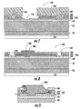
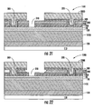
- a first dry etch (preferably anisotropic) can be used to selectively etch the dielectric layer 500 in the defined gate contact area 310.
- the first dry etch can be selective to AlGaN and the dielectric stack 200.
- a second isotropic etch of layer 210, selective to layers 220, the AlGaN layer 140, and the dielectric layer 500 can be performed.
- the second etch can also etch the dielectric layer 210 at a faster rate to provide under-cutting of dielectric 210 under the dielectric layer 500.
- Various types of etching can be used, for example, HF, a buffered oxide etchant (BOE) bath, isotropic dry etching using a downstream plasma etch technique, etc.
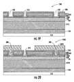
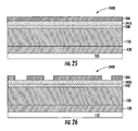
- a first dry etch can be used to selectively etch the dielectric layer 500 in the defined gate contact area 310.
- the first dry etch can be selective to AlGaN, AlN, and the dielectric stack 200.
- a second etch that is selective to the dielectric layer 500, the AlN layer 2410, and the AlGaN layer 140 can be performed.
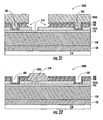
- the resulting structure is shown in FIG. 31 , which shows the gate contact area 310 including an exposed portion of the AlGaN layer 140 having approximately straight sidewalls formed from the AlN layer 2410 and an approximately wider bowl shaped area formed in the dielectric stack 200, with under-cutting under the dielectric layer 500.
- a recess can be etched into the AlGaN to form a recessed P- gate structure as shown in FIG. 33 .
- This recess etch can be performed to a depth of typically a fraction of the AlGaN thickness (about 5% to about 75%), depending on the device characteristics desired for the application, and can also be performed in the above discussed processes. Additional recess etches can also be performed in the source contact area and the drain contact area.
- FIG. 34 shows the resulting AlGaN P-gate 3200 structure.
- the method of the invention further comprises: masking the second dielectric to define the gate contact area.
- masking further defines a field plate area.
- etching the second dielectric further defines a lateral extension of an integrated field plate area.
- the method of the invention further comprises: growing the epitaxial p- type second compound semiconductor to substantially fill the etched first dielectric area and to cover at least a portion of the second dielectric.
- the method of the invention further comprises: forming an ohmic source contact over the source contact area; forming an ohmic drain contact over the drain contact area; and forming a Schottky metal over at least a portion of the epitaxial p- type second compound semiconductor.
- the formed ohmic source contact further forms a field plate.
- the formed Schottky metal further forms a field plate.
- etching the second dielectric to expose the gate contact area further comprises: recess etching at least a portion of the gate contact area through at least a portion of the second compound semiconductor layer.
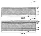
- the method of the invention further comprises: oxidizing the exposed AlN in the defined gate contact area to form a thin aluminum oxide layer; and growing epitaxial p-type III-V semiconductor on the thin aluminum oxide layer in the defined gate contact area to substantially fill the defined gate area
- oxidizing the exposed AlN further comprises: forming a thin oxidation layer of about 5 ⁇ to about 120 ⁇ .
- the thin oxidation layer is about 10 ⁇ to about 20 ⁇ .
- oxidizing the exposed AlN further comprises: applying an oxidizing process selected from the group consisting of thermal oxidation, rapid thermal anneal, and plasma enhanced oxidation.
Landscapes
- Junction Field-Effect Transistors (AREA)
- Insulated Gate Type Field-Effect Transistor (AREA)
Claims (19)
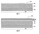
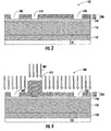
- Méthode de fabrication d'un transistor à haute mobilité d'électrons (HEMT) à mode d'enrichissement (mode e) comprenant :la formation d'une première couche de semi-conducteur composé sur une surface d'un substrat ;la formation d'une seconde couche de semi-conducteur composé sur une surface de la première couche de semi-conducteur composé opposée à la surface de substrat ;la formation d'un premier diélectrique sur une surface de la seconde couche de semi-conducteur composé opposée à la surface du premier semi-conducteur composé ;la définition d'une zone de contact source, d'une zone de contact de désamorçage, et d'une zone de contact de portillon, par le premier diélectrique en utilisant une couche de masque pour mettre en vue des parties de la seconde couche de semi-conducteur composé ;la formation d'un second diélectrique conformément via la premier diélectrique et les parties mises en vue de la seconde couche de semi-conducteur composé ;la gravure du second diélectrique pour mettre en vue la zone de portillon ;la gravure isotrope du premier diélectrique exposé dans la zone de contact de portillon pour constituer une zone gravée ;la production d'un second semi-conducteur composé de type p épitaxial sur la zone exposée de contact de portillon pour remplir de manière importante la zone de contact de portillon gravée et pour couvrir au moins une partie de la zone gravée du premier diélectrique.
- Méthode selon la revendication 1, comprenant par ailleurs : le masquage du second diélectrique pour définir la zone de contact de portillon.
- Méthode selon la revendication 2, dans laquelle le masquage définit par ailleurs une zone de plaque de champ.
- Méthode selon la revendication 1, dans laquelle la gravure du second diélectrique définit par ailleurs une extension latérale d'une zone de plaque de champ intégrée.
- Méthode selon la revendication 1, comprenant par ailleurs : la production du second semi-conducteur composé de type p épitaxial pour remplir de manière importante la première zone diélectrique gravée et pour couvrir au moins une partie de la second diélectrique.
- Méthode selon la revendication 1, comprenant par ailleurs : la formation d'un contact source ohmique via la zone de contact source ; la formation d'un contact de désamorçage ohmique via la zone de contact de désamorçage ; et la formation d'un métal de Schottky via au moins une
- Méthode selon la revendication 6, dans laquelle le contact source ohmique formé constitue par ailleurs une plaque de champ.
- Méthode selon la revendication 6, dans laquelle le métal de Schottky formé constitue par ailleurs une plaque de champ.
- Méthode selon la revendication 1, dans laquelle la gravure du second diélectrique pour mettre en vue la zone de contact de portillon comprend par ailleurs : la gravure cruciforme d'au moins une partie de la zone de contact de portillon par au moins une partie de la seconde couche de semi-conducteur composé.
- Méthode selon la revendication 1, dans laquelle le premier semi-conducteur composé comprend du GaN.
- Méthode selon la revendication 1, dans laquelle le substrat est sélectionné à partir du silicium, du saphir, du carbure de silicium, du phosphure d'indium, du diamant, du silicium sur du diamant, et du saphir sur du diamant.
- Méthode selon la revendication 1, comprenant par ailleurs : la formation d'une couche d'AlGaN entre la surface du substrat et la première couche de semi-conducteur composé.
- Méthode selon la revendication 1, dans laquelle la seconde couche de semi-conducteur composé comprend au moins un des composés AlGaN, GaN, InP, et InAlN.
- Méthode selon la revendication 1, dans laquelle la formation de la seconde couche de semi-conducteur composé, comprend par ailleurs : la formation d'un bloc semi-conducteur composé comprenant au moins deux couches différentes de semi-conducteurs composés.
- Méthode selon la revendication 14, dans laquelle bloc semi-conducteur comprend une couche d'AlGaN et une couche d'AlN.
- Méthode selon la revendication 1, dans laquelle la formation du second diélectrique comporte par ailleurs : la formation d'un nitrure au plasma comme seconde couche diélectrique.
- Méthode selon la revendication 1, comprenant par ailleurs : la formation d'une couche de couronnement entre la première couche diélectrique et la seconde couche de semi-conducteur composé, dans laquelle la couche de couronnement comprend une couche de GaN.
- Méthode selon la revendication 1, dans laquelle la formation du premier diélectrique comprend par ailleurs : la formation de plusieurs couches diélectriques.
- Méthode de fabrication d'un transistor à haute mobilité d'électrons (HEMT) à mode d'enrichissement (mode e) comprenant :la formation d'une première couche de semi-conducteur composé sur une surface d'un substrat ;la formation d'une seconde couche de semi-conducteur composé sur une surface de la première couche de semi-conducteur composé opposée à la surface de substrat ;la formation d'une troisième couche de semi-conducteur composé entre la seconde couche de semi-conducteur composé et un premier diélectrique ;la formation du premier diélectrique sur une surface de la troisième couche de semi-conducteur composé opposée à la surface de la seconde couche de semi-conducteur ;la définition d'une zone de contact source, d'une zone de contact de désamorçage, et d'une zone de contact de portillon, par le premier diélectrique en utilisant une couche de masque pour mettre en vue la couche de semi-conducteur AIN ;la formation d'un second diélectrique conformément via la premier diélectrique et les parties mises en vue de la troisième couche de semi-conducteur composé ;la gravure du second diélectrique et une partie du premier diélectrique pour mettre en vue le troisième semi-conducteur composé dans la zone de contact de portillon définie etla production d'un second semi-conducteur composé de type p épitaxial via la zone exposée de contact de portillon pour remplir de manière importante la zone de contact de portillon gravée et pour couvrir au moins une partie de la première zone diélectrique gravée.
Applications Claiming Priority (2)
| Application Number | Priority Date | Filing Date | Title |
|---|---|---|---|
| US28955309P | 2009-12-23 | 2009-12-23 | |
| US12/823,060 US8168486B2 (en) | 2009-06-24 | 2010-06-24 | Methods for manufacturing enhancement-mode HEMTs with self-aligned field plate |
Publications (3)
| Publication Number | Publication Date |
|---|---|
| EP2385544A2 EP2385544A2 (fr) | 2011-11-09 |
| EP2385544A3 EP2385544A3 (fr) | 2011-11-23 |
| EP2385544B1 true EP2385544B1 (fr) | 2013-02-13 |
Family
ID=44404077
Family Applications (1)
| Application Number | Title | Priority Date | Filing Date |
|---|---|---|---|
| EP20100196883 Not-in-force EP2385544B1 (fr) | 2009-12-23 | 2010-12-23 | Procédés de fabrication d'HEMT à mode d'enrichissement avec plaque de champ auto-alignée |
Country Status (4)
| Country | Link |
|---|---|
| EP (1) | EP2385544B1 (fr) |
| KR (1) | KR101168824B1 (fr) |
| CN (1) | CN102148157A (fr) |
| TW (1) | TWI380377B (fr) |
Families Citing this family (19)
| Publication number | Priority date | Publication date | Assignee | Title |
|---|---|---|---|---|
| KR101877427B1 (ko) * | 2011-11-15 | 2018-07-11 | 엘지이노텍 주식회사 | 반도체 소자 |
| US8884308B2 (en) * | 2011-11-29 | 2014-11-11 | Taiwan Semiconductor Manufacturing Company, Ltd. | High electron mobility transistor structure with improved breakdown voltage performance |
| EP2602827B1 (fr) * | 2011-12-09 | 2016-02-03 | Imec | Dispositif au nitrure du groupe III à mode d'enrichissement et son procédé de fabrication |
| CN102709321A (zh) * | 2012-04-20 | 2012-10-03 | 程凯 | 增强型开关器件及其制造方法 |
| US20140077266A1 (en) * | 2012-09-14 | 2014-03-20 | Power Integrations, Inc. | Heterostructure Transistor with Multiple Gate Dielectric Layers |
| JP6017248B2 (ja) | 2012-09-28 | 2016-10-26 | トランスフォーム・ジャパン株式会社 | 半導体装置の製造方法及び半導体装置 |
| WO2015009249A1 (fr) | 2013-07-17 | 2015-01-22 | Elektrotechnicky Ustav Sav | Transistor à enrichissement au iii-n à polarité n et son procédé de fabrication |
| CN104810264B (zh) * | 2014-01-26 | 2017-12-01 | 国家电网公司 | 一种基于ONO结构的SiC终端结构制备方法 |
| US10679860B2 (en) | 2015-03-09 | 2020-06-09 | Agency For Science, Technology And Research | Self-aligning source, drain and gate process for III-V nitride MISHEMTs |
| CN107293601B (zh) * | 2016-04-12 | 2021-10-22 | 朱江 | 一种肖特基半导体装置及其制备方法 |
| TWI664726B (zh) * | 2017-05-31 | 2019-07-01 | 財團法人工業技術研究院 | 歐姆接觸結構及具有此歐姆接觸結構之半導體元件 |
| EP4241308A1 (fr) * | 2020-12-20 | 2023-09-13 | Huawei Technologies Co., Ltd. | Transistor de puissance au nitrure de gallium |
| CN112864242A (zh) * | 2020-12-30 | 2021-05-28 | 南方科技大学 | 一种GaN器件及其制备方法 |
| CN114080691B (zh) * | 2021-09-28 | 2024-06-21 | 英诺赛科(苏州)科技有限公司 | 氮化物基半导体装置及其制造方法 |
| CN113793806A (zh) * | 2021-11-16 | 2021-12-14 | 深圳市时代速信科技有限公司 | 一种半导体器件及制备方法 |
| CN114068329B (zh) * | 2021-11-19 | 2025-10-10 | 苏州能屋电子科技有限公司 | 基于cmp刻蚀技术制备凹槽栅增强型hemt器件的方法 |
| CN114496754B (zh) * | 2021-12-31 | 2025-05-30 | 深圳市汇芯通信技术有限公司 | 一次光刻制作hemt的栅极、源极和漏极的方法 |
| TWI888870B (zh) * | 2023-07-19 | 2025-07-01 | 黃知澍 | 混合型氮化鋁鎵/氮化鎵高速電子遷移率電晶體裝置 |
| KR102903715B1 (ko) | 2025-01-10 | 2025-12-24 | 주식회사 사람과하이테크 | 황토 족욕 및 발 마사지기 |
Family Cites Families (6)
| Publication number | Priority date | Publication date | Assignee | Title |
|---|---|---|---|---|
| KR100590763B1 (ko) | 2003-12-03 | 2006-06-15 | 한국전자통신연구원 | 이종 접합을 갖는 고전자 이동도 트랜지스터의 제조방법 |
| US7547928B2 (en) * | 2004-06-30 | 2009-06-16 | Interuniversitair Microelektronica Centrum (Imec) | AlGaN/GaN high electron mobility transistor devices |
| US7655962B2 (en) * | 2007-02-23 | 2010-02-02 | Sensor Electronic Technology, Inc. | Enhancement mode insulated gate heterostructure field-effect transistor with electrically isolated RF-enhanced source contact |
| US8212290B2 (en) * | 2007-03-23 | 2012-07-03 | Cree, Inc. | High temperature performance capable gallium nitride transistor |
| JP2008249811A (ja) * | 2007-03-29 | 2008-10-16 | Nec Lcd Technologies Ltd | 液晶駆動回路、これを備える液晶表示装置及び駆動方法 |
| US7560325B1 (en) * | 2008-04-14 | 2009-07-14 | Semisouth Laboratories, Inc. | Methods of making lateral junction field effect transistors using selective epitaxial growth |
-
2010
- 2010-12-22 TW TW99145151A patent/TWI380377B/zh not_active IP Right Cessation
- 2010-12-23 EP EP20100196883 patent/EP2385544B1/fr not_active Not-in-force
- 2010-12-23 CN CN2010106210683A patent/CN102148157A/zh active Pending
- 2010-12-23 KR KR20100133316A patent/KR101168824B1/ko not_active Expired - Fee Related
Also Published As
| Publication number | Publication date |
|---|---|
| TW201133648A (en) | 2011-10-01 |
| EP2385544A3 (fr) | 2011-11-23 |
| KR20110073375A (ko) | 2011-06-29 |
| CN102148157A (zh) | 2011-08-10 |
| KR101168824B1 (ko) | 2012-07-25 |
| TWI380377B (en) | 2012-12-21 |
| EP2385544A2 (fr) | 2011-11-09 |
Similar Documents
| Publication | Publication Date | Title |
|---|---|---|
| EP2385544B1 (fr) | Procédés de fabrication d'HEMT à mode d'enrichissement avec plaque de champ auto-alignée | |
| US8168486B2 (en) | Methods for manufacturing enhancement-mode HEMTs with self-aligned field plate | |
| US12230690B2 (en) | Method of forming a high electron mobility transistor | |
| US10157994B2 (en) | High electron mobility transistor and method of forming the same | |
| US8399911B2 (en) | Enhancement mode field effect device and the method of production thereof | |
| US9236465B2 (en) | High electron mobility transistor and method of forming the same | |
| US8648390B2 (en) | Transistor with enhanced channel charge inducing material layer and threshold voltage control | |
| US9525052B2 (en) | Active area shaping of III-nitride devices utilizing a field plate defined by a dielectric body | |
| US8624296B1 (en) | High electron mobility transistor including an embedded flourine region | |
| TW201442230A (zh) | 異質結構功率電晶體以及製造異質結構半導體裝置的方法 | |
| KR20070032701A (ko) | 재성장된 오믹 콘택 영역을 갖는 질화물계 트랜지스터의제조방법 및 재성장된 오믹 콘택 영역을 갖는 질화물계트랜지스터 | |
| US8946778B2 (en) | Active area shaping of III-nitride devices utilizing steps of source-side and drain-side field plates | |
| US20140361310A1 (en) | Semiconductor structure and method of forming the same | |
| WO2022204913A1 (fr) | Dispositifs à semi-conducteurs au nitrure iii sur substrats à motifs | |
| EP1865561B1 (fr) | Dispositif à effet de champ en mode d'amélioration et son procédé de production | |
| US9318592B2 (en) | Active area shaping of III-nitride devices utilizing a source-side field plate and a wider drain-side field plate | |
| US9922936B1 (en) | Semiconductor lithography alignment feature with epitaxy blocker | |
| EP1883115A1 (fr) | Un dispositif à effet de champ en mode amélioré et sa méthode de production | |
| US8987784B2 (en) | Active area shaping of III-nitride devices utilizing multiple dielectric materials | |
| WO2024026816A1 (fr) | Dispositif à semi-conducteurs à base de nitrure et son procédé de fabrication | |
| CN115440811A (zh) | 半导体器件及其制造方法 |
Legal Events
| Date | Code | Title | Description |
|---|---|---|---|
| PUAL | Search report despatched |
Free format text: ORIGINAL CODE: 0009013 |
|
| AK | Designated contracting states |
Kind code of ref document: A2 Designated state(s): AL AT BE BG CH CY CZ DE DK EE ES FI FR GB GR HR HU IE IS IT LI LT LU LV MC MK MT NL NO PL PT RO RS SE SI SK SM TR |
|
| AX | Request for extension of the european patent |
Extension state: BA ME |
|
| AK | Designated contracting states |
Kind code of ref document: A3 Designated state(s): AL AT BE BG CH CY CZ DE DK EE ES FI FR GB GR HR HU IE IS IT LI LT LU LV MC MK MT NL NO PL PT RO RS SE SI SK SM TR |
|
| AX | Request for extension of the european patent |
Extension state: BA ME |
|
| PUAI | Public reference made under article 153(3) epc to a published international application that has entered the european phase |
Free format text: ORIGINAL CODE: 0009012 |
|
| RIC1 | Information provided on ipc code assigned before grant |
Ipc: H01L 29/423 20060101ALI20111020BHEP Ipc: H01L 29/778 20060101ALI20111020BHEP Ipc: H01L 21/335 20060101AFI20111020BHEP Ipc: H01L 29/40 20060101ALI20111020BHEP |
|
| 17P | Request for examination filed |
Effective date: 20120522 |
|
| GRAP | Despatch of communication of intention to grant a patent |
Free format text: ORIGINAL CODE: EPIDOSNIGR1 |
|
| GRAS | Grant fee paid |
Free format text: ORIGINAL CODE: EPIDOSNIGR3 |
|
| GRAA | (expected) grant |
Free format text: ORIGINAL CODE: 0009210 |
|
| AK | Designated contracting states |
Kind code of ref document: B1 Designated state(s): AL AT BE BG CH CY CZ DE DK EE ES FI FR GB GR HR HU IE IS IT LI LT LU LV MC MK MT NL NO PL PT RO RS SE SI SK SM TR |
|
| REG | Reference to a national code |
Ref country code: GB Ref legal event code: FG4D |
|
| REG | Reference to a national code |
Ref country code: AT Ref legal event code: REF Ref document number: 596886 Country of ref document: AT Kind code of ref document: T Effective date: 20130215 |
|
| REG | Reference to a national code |
Ref country code: IE Ref legal event code: FG4D |
|
| REG | Reference to a national code |
Ref country code: DE Ref legal event code: R096 Ref document number: 602010004977 Country of ref document: DE Effective date: 20130411 |
|
| REG | Reference to a national code |
Ref country code: AT Ref legal event code: MK05 Ref document number: 596886 Country of ref document: AT Kind code of ref document: T Effective date: 20130213 |
|
| REG | Reference to a national code |
Ref country code: NL Ref legal event code: VDEP Effective date: 20130213 |
|
| REG | Reference to a national code |
Ref country code: LT Ref legal event code: MG4D |
|
| PG25 | Lapsed in a contracting state [announced via postgrant information from national office to epo] |
Ref country code: BG Free format text: LAPSE BECAUSE OF FAILURE TO SUBMIT A TRANSLATION OF THE DESCRIPTION OR TO PAY THE FEE WITHIN THE PRESCRIBED TIME-LIMIT Effective date: 20130513 Ref country code: LT Free format text: LAPSE BECAUSE OF FAILURE TO SUBMIT A TRANSLATION OF THE DESCRIPTION OR TO PAY THE FEE WITHIN THE PRESCRIBED TIME-LIMIT Effective date: 20130213 Ref country code: NO Free format text: LAPSE BECAUSE OF FAILURE TO SUBMIT A TRANSLATION OF THE DESCRIPTION OR TO PAY THE FEE WITHIN THE PRESCRIBED TIME-LIMIT Effective date: 20130513 Ref country code: AT Free format text: LAPSE BECAUSE OF FAILURE TO SUBMIT A TRANSLATION OF THE DESCRIPTION OR TO PAY THE FEE WITHIN THE PRESCRIBED TIME-LIMIT Effective date: 20130213 Ref country code: IS Free format text: LAPSE BECAUSE OF FAILURE TO SUBMIT A TRANSLATION OF THE DESCRIPTION OR TO PAY THE FEE WITHIN THE PRESCRIBED TIME-LIMIT Effective date: 20130613 Ref country code: ES Free format text: LAPSE BECAUSE OF FAILURE TO SUBMIT A TRANSLATION OF THE DESCRIPTION OR TO PAY THE FEE WITHIN THE PRESCRIBED TIME-LIMIT Effective date: 20130524 Ref country code: SE Free format text: LAPSE BECAUSE OF FAILURE TO SUBMIT A TRANSLATION OF THE DESCRIPTION OR TO PAY THE FEE WITHIN THE PRESCRIBED TIME-LIMIT Effective date: 20130213 |
|
| PG25 | Lapsed in a contracting state [announced via postgrant information from national office to epo] |
Ref country code: LV Free format text: LAPSE BECAUSE OF FAILURE TO SUBMIT A TRANSLATION OF THE DESCRIPTION OR TO PAY THE FEE WITHIN THE PRESCRIBED TIME-LIMIT Effective date: 20130213 Ref country code: PL Free format text: LAPSE BECAUSE OF FAILURE TO SUBMIT A TRANSLATION OF THE DESCRIPTION OR TO PAY THE FEE WITHIN THE PRESCRIBED TIME-LIMIT Effective date: 20130213 Ref country code: PT Free format text: LAPSE BECAUSE OF FAILURE TO SUBMIT A TRANSLATION OF THE DESCRIPTION OR TO PAY THE FEE WITHIN THE PRESCRIBED TIME-LIMIT Effective date: 20130613 Ref country code: BE Free format text: LAPSE BECAUSE OF FAILURE TO SUBMIT A TRANSLATION OF THE DESCRIPTION OR TO PAY THE FEE WITHIN THE PRESCRIBED TIME-LIMIT Effective date: 20130213 Ref country code: FI Free format text: LAPSE BECAUSE OF FAILURE TO SUBMIT A TRANSLATION OF THE DESCRIPTION OR TO PAY THE FEE WITHIN THE PRESCRIBED TIME-LIMIT Effective date: 20130213 Ref country code: GR Free format text: LAPSE BECAUSE OF FAILURE TO SUBMIT A TRANSLATION OF THE DESCRIPTION OR TO PAY THE FEE WITHIN THE PRESCRIBED TIME-LIMIT Effective date: 20130514 Ref country code: SI Free format text: LAPSE BECAUSE OF FAILURE TO SUBMIT A TRANSLATION OF THE DESCRIPTION OR TO PAY THE FEE WITHIN THE PRESCRIBED TIME-LIMIT Effective date: 20130213 |
|
| PG25 | Lapsed in a contracting state [announced via postgrant information from national office to epo] |
Ref country code: RS Free format text: LAPSE BECAUSE OF FAILURE TO SUBMIT A TRANSLATION OF THE DESCRIPTION OR TO PAY THE FEE WITHIN THE PRESCRIBED TIME-LIMIT Effective date: 20130213 Ref country code: HR Free format text: LAPSE BECAUSE OF FAILURE TO SUBMIT A TRANSLATION OF THE DESCRIPTION OR TO PAY THE FEE WITHIN THE PRESCRIBED TIME-LIMIT Effective date: 20130213 |
|
| PG25 | Lapsed in a contracting state [announced via postgrant information from national office to epo] |
Ref country code: NL Free format text: LAPSE BECAUSE OF FAILURE TO SUBMIT A TRANSLATION OF THE DESCRIPTION OR TO PAY THE FEE WITHIN THE PRESCRIBED TIME-LIMIT Effective date: 20130213 Ref country code: RO Free format text: LAPSE BECAUSE OF FAILURE TO SUBMIT A TRANSLATION OF THE DESCRIPTION OR TO PAY THE FEE WITHIN THE PRESCRIBED TIME-LIMIT Effective date: 20130213 Ref country code: EE Free format text: LAPSE BECAUSE OF FAILURE TO SUBMIT A TRANSLATION OF THE DESCRIPTION OR TO PAY THE FEE WITHIN THE PRESCRIBED TIME-LIMIT Effective date: 20130213 Ref country code: SK Free format text: LAPSE BECAUSE OF FAILURE TO SUBMIT A TRANSLATION OF THE DESCRIPTION OR TO PAY THE FEE WITHIN THE PRESCRIBED TIME-LIMIT Effective date: 20130213 Ref country code: DK Free format text: LAPSE BECAUSE OF FAILURE TO SUBMIT A TRANSLATION OF THE DESCRIPTION OR TO PAY THE FEE WITHIN THE PRESCRIBED TIME-LIMIT Effective date: 20130213 Ref country code: CZ Free format text: LAPSE BECAUSE OF FAILURE TO SUBMIT A TRANSLATION OF THE DESCRIPTION OR TO PAY THE FEE WITHIN THE PRESCRIBED TIME-LIMIT Effective date: 20130213 |
|
| PLBE | No opposition filed within time limit |
Free format text: ORIGINAL CODE: 0009261 |
|
| STAA | Information on the status of an ep patent application or granted ep patent |
Free format text: STATUS: NO OPPOSITION FILED WITHIN TIME LIMIT |
|
| PG25 | Lapsed in a contracting state [announced via postgrant information from national office to epo] |
Ref country code: IT Free format text: LAPSE BECAUSE OF FAILURE TO SUBMIT A TRANSLATION OF THE DESCRIPTION OR TO PAY THE FEE WITHIN THE PRESCRIBED TIME-LIMIT Effective date: 20130213 |
|
| 26N | No opposition filed |
Effective date: 20131114 |
|
| REG | Reference to a national code |
Ref country code: DE Ref legal event code: R097 Ref document number: 602010004977 Country of ref document: DE Effective date: 20131114 |
|
| REG | Reference to a national code |
Ref country code: DE Ref legal event code: R119 Ref document number: 602010004977 Country of ref document: DE |
|
| PG25 | Lapsed in a contracting state [announced via postgrant information from national office to epo] |
Ref country code: LU Free format text: LAPSE BECAUSE OF FAILURE TO SUBMIT A TRANSLATION OF THE DESCRIPTION OR TO PAY THE FEE WITHIN THE PRESCRIBED TIME-LIMIT Effective date: 20131223 |
|
| REG | Reference to a national code |
Ref country code: DE Ref legal event code: R119 Ref document number: 602010004977 Country of ref document: DE Effective date: 20140701 |
|
| REG | Reference to a national code |
Ref country code: IE Ref legal event code: MM4A |
|
| REG | Reference to a national code |
Ref country code: FR Ref legal event code: ST Effective date: 20140829 |
|
| PG25 | Lapsed in a contracting state [announced via postgrant information from national office to epo] |
Ref country code: IE Free format text: LAPSE BECAUSE OF NON-PAYMENT OF DUE FEES Effective date: 20131223 Ref country code: DE Free format text: LAPSE BECAUSE OF NON-PAYMENT OF DUE FEES Effective date: 20140701 |
|
| PG25 | Lapsed in a contracting state [announced via postgrant information from national office to epo] |
Ref country code: FR Free format text: LAPSE BECAUSE OF NON-PAYMENT OF DUE FEES Effective date: 20131231 |
|
| PG25 | Lapsed in a contracting state [announced via postgrant information from national office to epo] |
Ref country code: MC Free format text: LAPSE BECAUSE OF FAILURE TO SUBMIT A TRANSLATION OF THE DESCRIPTION OR TO PAY THE FEE WITHIN THE PRESCRIBED TIME-LIMIT Effective date: 20130213 |
|
| PG25 | Lapsed in a contracting state [announced via postgrant information from national office to epo] |
Ref country code: SM Free format text: LAPSE BECAUSE OF FAILURE TO SUBMIT A TRANSLATION OF THE DESCRIPTION OR TO PAY THE FEE WITHIN THE PRESCRIBED TIME-LIMIT Effective date: 20130213 |
|
| PG25 | Lapsed in a contracting state [announced via postgrant information from national office to epo] |
Ref country code: CY Free format text: LAPSE BECAUSE OF FAILURE TO SUBMIT A TRANSLATION OF THE DESCRIPTION OR TO PAY THE FEE WITHIN THE PRESCRIBED TIME-LIMIT Effective date: 20130213 Ref country code: TR Free format text: LAPSE BECAUSE OF FAILURE TO SUBMIT A TRANSLATION OF THE DESCRIPTION OR TO PAY THE FEE WITHIN THE PRESCRIBED TIME-LIMIT Effective date: 20130213 |
|
| PG25 | Lapsed in a contracting state [announced via postgrant information from national office to epo] |
Ref country code: HU Free format text: LAPSE BECAUSE OF FAILURE TO SUBMIT A TRANSLATION OF THE DESCRIPTION OR TO PAY THE FEE WITHIN THE PRESCRIBED TIME-LIMIT; INVALID AB INITIO Effective date: 20101223 Ref country code: MK Free format text: LAPSE BECAUSE OF FAILURE TO SUBMIT A TRANSLATION OF THE DESCRIPTION OR TO PAY THE FEE WITHIN THE PRESCRIBED TIME-LIMIT Effective date: 20130213 |
|
| REG | Reference to a national code |
Ref country code: CH Ref legal event code: PL |
|
| GBPC | Gb: european patent ceased through non-payment of renewal fee |
Effective date: 20141223 |
|
| PG25 | Lapsed in a contracting state [announced via postgrant information from national office to epo] |
Ref country code: MT Free format text: LAPSE BECAUSE OF FAILURE TO SUBMIT A TRANSLATION OF THE DESCRIPTION OR TO PAY THE FEE WITHIN THE PRESCRIBED TIME-LIMIT Effective date: 20130213 |
|
| PG25 | Lapsed in a contracting state [announced via postgrant information from national office to epo] |
Ref country code: LI Free format text: LAPSE BECAUSE OF NON-PAYMENT OF DUE FEES Effective date: 20141231 Ref country code: GB Free format text: LAPSE BECAUSE OF NON-PAYMENT OF DUE FEES Effective date: 20141223 Ref country code: CH Free format text: LAPSE BECAUSE OF NON-PAYMENT OF DUE FEES Effective date: 20141231 |
|
| PG25 | Lapsed in a contracting state [announced via postgrant information from national office to epo] |
Ref country code: AL Free format text: LAPSE BECAUSE OF FAILURE TO SUBMIT A TRANSLATION OF THE DESCRIPTION OR TO PAY THE FEE WITHIN THE PRESCRIBED TIME-LIMIT Effective date: 20130213 |