EP2387085A1 - Organische lichtemittierende Diode und Lichtquellenvorrichtung damit - Google Patents
Organische lichtemittierende Diode und Lichtquellenvorrichtung damit Download PDFInfo
- Publication number
- EP2387085A1 EP2387085A1 EP11164715A EP11164715A EP2387085A1 EP 2387085 A1 EP2387085 A1 EP 2387085A1 EP 11164715 A EP11164715 A EP 11164715A EP 11164715 A EP11164715 A EP 11164715A EP 2387085 A1 EP2387085 A1 EP 2387085A1
- Authority
- EP
- European Patent Office
- Prior art keywords
- transparent resin
- refractive index
- output
- side substrate
- layer
- Prior art date
- Legal status (The legal status is an assumption and is not a legal conclusion. Google has not performed a legal analysis and makes no representation as to the accuracy of the status listed.)
- Withdrawn
Links
- 239000010410 layer Substances 0.000 claims abstract description 204
- 239000000758 substrate Substances 0.000 claims abstract description 140
- 239000002245 particle Substances 0.000 claims abstract description 119
- 239000012044 organic layer Substances 0.000 claims abstract description 84
- 238000000149 argon plasma sintering Methods 0.000 claims abstract description 41
- 239000000463 material Substances 0.000 claims abstract description 25
- 239000011347 resin Substances 0.000 claims description 222
- 229920005989 resin Polymers 0.000 claims description 222
- 239000010409 thin film Substances 0.000 description 69
- 239000010408 film Substances 0.000 description 51
- 239000010419 fine particle Substances 0.000 description 31
- 238000000605 extraction Methods 0.000 description 29
- 230000000694 effects Effects 0.000 description 26
- 230000009467 reduction Effects 0.000 description 18
- 238000010586 diagram Methods 0.000 description 15
- 238000004088 simulation Methods 0.000 description 15
- 239000003570 air Substances 0.000 description 14
- 239000004925 Acrylic resin Substances 0.000 description 10
- 229910052782 aluminium Inorganic materials 0.000 description 8
- XAGFODPZIPBFFR-UHFFFAOYSA-N aluminium Chemical compound [Al] XAGFODPZIPBFFR-UHFFFAOYSA-N 0.000 description 8
- 229920000178 Acrylic resin Polymers 0.000 description 7
- 230000005525 hole transport Effects 0.000 description 7
- 239000005020 polyethylene terephthalate Substances 0.000 description 7
- 229920000139 polyethylene terephthalate Polymers 0.000 description 7
- 239000012080 ambient air Substances 0.000 description 6
- 238000000034 method Methods 0.000 description 6
- 239000011521 glass Substances 0.000 description 5
- DOIRQSBPFJWKBE-UHFFFAOYSA-N dibutyl phthalate Chemical compound CCCCOC(=O)C1=CC=CC=C1C(=O)OCCCC DOIRQSBPFJWKBE-UHFFFAOYSA-N 0.000 description 4
- 239000000843 powder Substances 0.000 description 4
- GWEVSGVZZGPLCZ-UHFFFAOYSA-N Titan oxide Chemical compound O=[Ti]=O GWEVSGVZZGPLCZ-UHFFFAOYSA-N 0.000 description 3
- 229910002113 barium titanate Inorganic materials 0.000 description 3
- JRPBQTZRNDNNOP-UHFFFAOYSA-N barium titanate Chemical compound [Ba+2].[Ba+2].[O-][Ti]([O-])([O-])[O-] JRPBQTZRNDNNOP-UHFFFAOYSA-N 0.000 description 3
- 239000000203 mixture Substances 0.000 description 3
- RVTZCBVAJQQJTK-UHFFFAOYSA-N oxygen(2-);zirconium(4+) Chemical compound [O-2].[O-2].[Zr+4] RVTZCBVAJQQJTK-UHFFFAOYSA-N 0.000 description 3
- -1 polyethylene terephthalate Polymers 0.000 description 3
- OGIDPMRJRNCKJF-UHFFFAOYSA-N titanium oxide Inorganic materials [Ti]=O OGIDPMRJRNCKJF-UHFFFAOYSA-N 0.000 description 3
- 229910001928 zirconium oxide Inorganic materials 0.000 description 3
- XKRFYHLGVUSROY-UHFFFAOYSA-N Argon Chemical compound [Ar] XKRFYHLGVUSROY-UHFFFAOYSA-N 0.000 description 2
- OKTJSMMVPCPJKN-UHFFFAOYSA-N Carbon Chemical compound [C] OKTJSMMVPCPJKN-UHFFFAOYSA-N 0.000 description 2
- 230000008901 benefit Effects 0.000 description 2
- 229910052799 carbon Inorganic materials 0.000 description 2
- 230000008859 change Effects 0.000 description 2
- 239000000470 constituent Substances 0.000 description 2
- 238000009826 distribution Methods 0.000 description 2
- 229920001971 elastomer Polymers 0.000 description 2
- 238000005401 electroluminescence Methods 0.000 description 2
- 229910003437 indium oxide Inorganic materials 0.000 description 2
- PJXISJQVUVHSOJ-UHFFFAOYSA-N indium(iii) oxide Chemical compound [O-2].[O-2].[O-2].[In+3].[In+3] PJXISJQVUVHSOJ-UHFFFAOYSA-N 0.000 description 2
- AMGQUBHHOARCQH-UHFFFAOYSA-N indium;oxotin Chemical compound [In].[Sn]=O AMGQUBHHOARCQH-UHFFFAOYSA-N 0.000 description 2
- 239000000395 magnesium oxide Substances 0.000 description 2
- CPLXHLVBOLITMK-UHFFFAOYSA-N magnesium oxide Inorganic materials [Mg]=O CPLXHLVBOLITMK-UHFFFAOYSA-N 0.000 description 2
- AXZKOIWUVFPNLO-UHFFFAOYSA-N magnesium;oxygen(2-) Chemical compound [O-2].[Mg+2] AXZKOIWUVFPNLO-UHFFFAOYSA-N 0.000 description 2
- 238000005259 measurement Methods 0.000 description 2
- 229910052751 metal Inorganic materials 0.000 description 2
- 239000002184 metal Substances 0.000 description 2
- IBHBKWKFFTZAHE-UHFFFAOYSA-N n-[4-[4-(n-naphthalen-1-ylanilino)phenyl]phenyl]-n-phenylnaphthalen-1-amine Chemical group C1=CC=CC=C1N(C=1C2=CC=CC=C2C=CC=1)C1=CC=C(C=2C=CC(=CC=2)N(C=2C=CC=CC=2)C=2C3=CC=CC=C3C=CC=2)C=C1 IBHBKWKFFTZAHE-UHFFFAOYSA-N 0.000 description 2
- 229920001084 poly(chloroprene) Polymers 0.000 description 2
- 230000008569 process Effects 0.000 description 2
- YVTHLONGBIQYBO-UHFFFAOYSA-N zinc indium(3+) oxygen(2-) Chemical compound [O--].[Zn++].[In+3] YVTHLONGBIQYBO-UHFFFAOYSA-N 0.000 description 2
- OGGKVJMNFFSDEV-UHFFFAOYSA-N 3-methyl-n-[4-[4-(n-(3-methylphenyl)anilino)phenyl]phenyl]-n-phenylaniline Chemical compound CC1=CC=CC(N(C=2C=CC=CC=2)C=2C=CC(=CC=2)C=2C=CC(=CC=2)N(C=2C=CC=CC=2)C=2C=C(C)C=CC=2)=C1 OGGKVJMNFFSDEV-UHFFFAOYSA-N 0.000 description 1
- 239000004593 Epoxy Substances 0.000 description 1
- YCKRFDGAMUMZLT-UHFFFAOYSA-N Fluorine atom Chemical compound [F] YCKRFDGAMUMZLT-UHFFFAOYSA-N 0.000 description 1
- 239000004642 Polyimide Substances 0.000 description 1
- ATJFFYVFTNAWJD-UHFFFAOYSA-N Tin Chemical compound [Sn] ATJFFYVFTNAWJD-UHFFFAOYSA-N 0.000 description 1
- HCHKCACWOHOZIP-UHFFFAOYSA-N Zinc Chemical compound [Zn] HCHKCACWOHOZIP-UHFFFAOYSA-N 0.000 description 1
- NIXOWILDQLNWCW-UHFFFAOYSA-N acrylic acid group Chemical group C(C=C)(=O)O NIXOWILDQLNWCW-UHFFFAOYSA-N 0.000 description 1
- 230000002411 adverse Effects 0.000 description 1
- 230000004075 alteration Effects 0.000 description 1
- 229910052786 argon Inorganic materials 0.000 description 1
- 239000003086 colorant Substances 0.000 description 1
- 238000011109 contamination Methods 0.000 description 1
- 230000006866 deterioration Effects 0.000 description 1
- 239000003822 epoxy resin Substances 0.000 description 1
- 229910052731 fluorine Inorganic materials 0.000 description 1
- 239000011737 fluorine Substances 0.000 description 1
- 239000006260 foam Substances 0.000 description 1
- 238000005187 foaming Methods 0.000 description 1
- 239000007789 gas Substances 0.000 description 1
- 230000006872 improvement Effects 0.000 description 1
- 239000004973 liquid crystal related substance Substances 0.000 description 1
- 238000004519 manufacturing process Methods 0.000 description 1
- 230000004048 modification Effects 0.000 description 1
- 238000012986 modification Methods 0.000 description 1
- 238000000465 moulding Methods 0.000 description 1
- 230000003287 optical effect Effects 0.000 description 1
- 238000001579 optical reflectometry Methods 0.000 description 1
- 238000005457 optimization Methods 0.000 description 1
- 239000011368 organic material Substances 0.000 description 1
- TWNQGVIAIRXVLR-UHFFFAOYSA-N oxo(oxoalumanyloxy)alumane Chemical compound O=[Al]O[Al]=O TWNQGVIAIRXVLR-UHFFFAOYSA-N 0.000 description 1
- 239000004033 plastic Substances 0.000 description 1
- 229920003023 plastic Polymers 0.000 description 1
- 239000004014 plasticizer Substances 0.000 description 1
- 230000010287 polarization Effects 0.000 description 1
- 229920000647 polyepoxide Polymers 0.000 description 1
- 229920006267 polyester film Polymers 0.000 description 1
- 229920001721 polyimide Polymers 0.000 description 1
- 238000003825 pressing Methods 0.000 description 1
- 230000002265 prevention Effects 0.000 description 1
- 238000002310 reflectometry Methods 0.000 description 1
- 230000003014 reinforcing effect Effects 0.000 description 1
- 230000003252 repetitive effect Effects 0.000 description 1
- 239000005394 sealing glass Substances 0.000 description 1
- 239000002210 silicon-based material Substances 0.000 description 1
- 229920002379 silicone rubber Polymers 0.000 description 1
- 229910052709 silver Inorganic materials 0.000 description 1
- 239000004332 silver Substances 0.000 description 1
- 239000007787 solid Substances 0.000 description 1
- 230000007480 spreading Effects 0.000 description 1
- 238000003892 spreading Methods 0.000 description 1
- 238000004544 sputter deposition Methods 0.000 description 1
- 229910052725 zinc Inorganic materials 0.000 description 1
- 239000011701 zinc Substances 0.000 description 1
Images










Classifications
-
- H—ELECTRICITY
- H10—SEMICONDUCTOR DEVICES; ELECTRIC SOLID-STATE DEVICES NOT OTHERWISE PROVIDED FOR
- H10K—ORGANIC ELECTRIC SOLID-STATE DEVICES
- H10K50/00—Organic light-emitting devices
- H10K50/80—Constructional details
- H10K50/85—Arrangements for extracting light from the devices
- H10K50/854—Arrangements for extracting light from the devices comprising scattering means
-
- H—ELECTRICITY
- H10—SEMICONDUCTOR DEVICES; ELECTRIC SOLID-STATE DEVICES NOT OTHERWISE PROVIDED FOR
- H10K—ORGANIC ELECTRIC SOLID-STATE DEVICES
- H10K50/00—Organic light-emitting devices
- H10K50/80—Constructional details
- H10K50/85—Arrangements for extracting light from the devices
- H10K50/858—Arrangements for extracting light from the devices comprising refractive means, e.g. lenses
Definitions
- the present invention relates to an organic light emitting diode and a light source device using the same.
- JP-A-2004-296423 discloses therein a technique which follows.
- An objective of this prior art is to provide an organic electroluminescence device capable of efficiently extracting loss light which was confined within the device as waveguide light to thereby improve external light extraction efficiency.
- the prior art relates to an organic electroluminescence device of the type having at least one organic layer, including a light emission layer, and a pair of electrodes consisting essentially of a reflective electrode and a transparent electrode with the organic layer being sandwiched therebetween.
- constituents are formed in such a manner that a front-face luminance value of emission light to be irradiated from a light extraction surface toward the observer side and luminance values in those directions of 50 to 70 degrees satisfy the following relationship: front-face luminance value ⁇ luminance values in 50-70 degree directions.
- the device is characterized by providing a region which generates turbulence in reflection and refraction angles of light while the light emitted from the emission layer exits to the observer side through the transparent electrode.
- a problem faced with the prior art device is that the light extraction efficiency is kept low because of the fact that total reflection can take place at interfaces of respective layers constituting an organic light emitting diode. It is therefore an object of the present invention to improve the light extraction efficiency in the organic light emitting diode and a light source device using this diode.
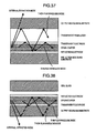
- a structure of organic light emitting diode (OLED) shown in Fig. 37 is as follows.
- An organic layer composed of organic molecules is formed on a reflection electrode which is formed on a reflection-side electrode.
- a transparent electrode is formed, which is made of indium oxide with a slight amount of tin added thereto, i.e., indium-tin-oxide (ITO), or indium oxide with a small amount of zinc added thereto, i.e., indium-zinc-oxide (IZO).
- ITO indium-tin-oxide
- IZO indium-zinc-oxide
- a transparent resin layer is disposed on the transparent electrode, with an output-side substrate being situated on the transparent resin layer.
- This structure is generally known as the top emission type.
- an OLED structure shown in Fig. 38 is as follows.
- a transparent electrode is placed on an output-side substrate.
- An organic layer is formed on the transparent electrode.
- a reflection electrode is formed on the organic layer.
- a sealing glass plate for use as a reflection-side substrate is disposed above the reflection electrode with a vacuum or an inactive gas-filled layer being situated between the electrode and the glass plate.
- This structure is commonly called the bottom emission type. Both the top emission type and the bottom emission type are arranged to illuminate an exterior space by causing the light that was produced within the organic layer to go out of the output-side substrate.
- the reflection electrode is typically made of aluminum.
- a layer called the electron transportation layer is formed on the reflection electrode; a hole transport layer is formed on the transparent electrode side.
- a layer called the light emission layer or emissive layer is formed between the electron transport layer and the hole transport layer. Electrons and holes are recombined together in a region of about 10 nanometers (nm) in close proximity to either an interface between the emissive layer and electron transport layer or an interface between the emissive layer and hole transport layer; thus, the organic layer emits light.
- the refractive index of the organic layer is typically about 1.8.
- the refractive index of the transparent electrode is about 2.0.
- the refractive index of the transparent resin layer is about 1.5.
- the refractive index of the output-side substrate is 1.5 or more or less.
- the light produced at the luminous point passes through the transparent electrode, transparent resin layer and output-side substrate and then exits to the exterior.
- the transparent electrode, transparent resin layer and output-side substrate In the case of the top emission type, reflection occurs at the interface between the transparent electrode and transparent resin layer and at the interface between the transparent resin layer and output-side substrate and also at the interface between the output-side substrate and ambient air; so, the amount of light to be actually taken out to the exterior becomes extremely low.
- reflection occurs at the interface between the transparent electrode and output-side substrate and the interface between the output-side substrate and air so that the amount of light to be extracted to the outside becomes very low.
- the thin-film waveguide mode Light incapable of being brought out into the output-side substrate due to the influence of total reflection is called the thin-film waveguide mode. Additionally, the light that was emitted at the luminous point is divided into light which goes for the transparent electrode side and light which goes for the transparent electrode side after having once reflected at the reflection electrode. In this case, upon failure to properly control interference conditions of these two kinds of light rays, the thin-film waveguide mode increases undesirably.
- the thick-film waveguide mode light that is totally reflected at the interface between the output-side substrate and ambient air and thus cannot be extracted into the air.
- the external extraction mode light which was actually brought out or extracted to the air.
- Embodiments as will be described later are the ones that have been made to solve the above-stated problem to thereby provide a technique capable of reducing both the thin-film waveguide mode and the thick-film waveguide mode in OLED devices, thus making it possible to obtain highly enhanced light extraction efficiency.
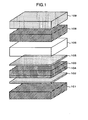
- Fig. 1 is a diagram showing an exploded perspective view of an organic light emitting diode (OLED) device in accordance with one embodiment of this invention.
- Fig. 2 is a diagram showing, in cross-section, a structure of the OLED of this embodiment.
- the OLED of this embodiment has a reflection-side substrate 101, aluminum reflection electrode 102, organic layer 103, transparent electrode 105 made of indium-tin-oxide (ITO) or indium-zinc-oxide (IZO), first transparent resin layer 106, output-side substrate 108, and light scattering layer 109.
- ITO indium-tin-oxide
- IZO indium-zinc-oxide
- a direction in which light travels from the reflection-side substrate 101 toward the output-side substrate 108 is set as the direction of light extraction from the organic layer 103.
- the reflection-side substrate 101 and output-side substrate 108 may typically be made of glass or plastic substrate materials (such as polychloroprene, polyethylene terephthalate (PET) or the like). In a viewpoint of prevention of contamination of the organic layer, it is desirable that the reflection-side substrate 101 and output-side substrate 108 be made of glass.
- the reflection electrode 102 is formed on the reflection-side substrate 101. On the reflection electrode 102, the organic layer 103 composed of organic molecules is formed.
- the organic layer 103 has its refractive index of about 1.8; practically, it is greater than or equal to 1.7 and less than or equal to 1.9.
- the organic layer 103 involves a luminous point 104.
- the transparent electrode 105 is formed on the organic layer 103.
- the refractive index of the transparent electrode 105 is about 2.0; practically, it falls within a range of from 1.95 to 2.05.
- the first transparent resin layer 106 is disposed on the transparent electrode 105.
- the reflection electrode 102 functions to reflect the light emitted by the organic layer 103.
- a reflector plate with optical reflectivity and the transparent electrode 105 may be used.
- the reflector plate is formed on the reflection-side substrate 101, with the transparent electrode 105 being formed on the reflector plate.
- the reflector plate is an argon (Ar) substrate.
- the first transparent resin layer 106 is in contact with the transparent electrode 105 and output-side substrate 108.
- the first transparent resin layer 106 is made of acrylic resin, for example. By dispersing fine particles 110 of titanium oxide in the acrylic resin for use as a base material, it is possible to control the refractive index of the first transparent resin layer 106.
- the refractive index of first transparent resin layer 106 is settable to a given value selected from a range of from about 1.5 to 2.2.
- Examples of the base material of the first transparent resin layer 106 are transparent resin materials with adhesivity, including but not limited to polyethylene terephthalate (PET), silicon-based materials, acrylic materials, polyimide and epoxy.
- PET polyethylene terephthalate
- the output-side substrate 108 is situated on the first transparent resin layer 106.
- the refractive index of the output-side substrate 108 is about 1.5; practically, its value falls within a range of 1.50 to 1.56.
- the light scattering layer 109 is placed on the output-side substrate 108.
- the light scattering layer 109 may not be formed on an entire surface of the output-side substrate 108 as shown in Fig. 1 .
- the light scattering layer 109 is designed to be less in area than the output-side substrate 108 in an inplane direction(s) of the output-side substrate 108, thereby enabling improvement of productivity.
- the light scattering layer 109 is made of an acrylic resin for use as its base material, which contains fine particles 110 of zirconium oxide dispersed therein.
- the base material is optically transparent and has adhesiveness.
- the refractive index of the base material of light scattering layer 109 is close in value to the refractive index of glass; more preferably, the former refractive index is the same as the latter.
- the recitation "the refractive index is the same" means a degree of sameness capable of attaining the intended effects of this embodiment; it does not require achievement of the exact equality in a strict sense. In practical implementation, the refractive indexes may be determined so that a difference therebetween is within a value of 0.1; more preferably, within 0.05.
- the base material of the light scattering layer 109 may alternatively be made of epoxy resin or PET other than the acrylic resin. Practical examples of the material of the fine particles 110 other than the zirconium oxide are barium titanate, aluminum oxide, etc.
- the fine particles 110 may be composed of a single kind of material selected from the above-stated examples or, alternatively, two or more kinds of materials.
- the refractive index of the acrylic resin is about 1.5, which is the same as the refractive index of the output-side substrate 108. It should be noted that the refractive index of each layer is measured, for example, by an optical thin-film measurement system FilmTek3000 (manufactured by YA-MAN, Ltd.) at room temperatures.
- the OLED shown in Fig. 1 is used to provide a light source apparatus which includes a drive device for driving the OLED.
- the refractive index of the transparent electrode 105 is greater than the refractive index of the first transparent resin layer 106.
- the refractive index of the first transparent resin layer 106 is the same as the refractive index of the output-side substrate 108.
- the refractive index of the output-side substrate 108 is higher than the refractive index of ambient air.
- the refractive index of the fine particles 110 contained in the light scattering layer 109 is higher than the refractive index of the base material of the light scattering layer and that of the output-side substrate 108.
- the refractive index of the first transparent resin layer 106 is almost equal to the refractive index of the output-side substrate 108; so, this is equivalent to the state that there is substantially no interface between the first transparent resin layer 106 and output-side substrate 108.
- the structure shown in Fig. 1 is deemed equivalent to a structure with lack of the first transparent resin layer 106 and also with the transparent electrode 105 and output-side substrate 108 being brought into direct contact with each other.
- the light scattering layer 109 is situated on a side which is opposite to the existence side of the transparent electrode 105 with respect to the output-side substrate 108, the light scattering layer 109 may alternatively be placed between the output-side substrate 108 and the transparent electrode 105.
- the light scattering layer 109 By disposing the light scattering layer 109 between the output-side substrate 108 and transparent electrode 105, it is possible to protect the light scattering layer 109 by the output-side substrate 108 that is robust against deterioration.
- the light scattering layer 109 is fabricated, it sometimes happens that a concavo-convex configuration is formed on the surface of the light scattering layer 109. Accordingly, by disposing the light scattering layer 109 on the opposite side to the transparent electrode 105's existence side with respect to the output-side substrate 108, the surface of the light scattering layer 109 on the concave-convex configuration-existing side is no longer contacted with the output-side substrate 108, thereby improving the productivity. In either case, the light scattering layer 109 is in contact with the output-side substrate 108.
- the first transparent resin layer 106 shown in Fig. 1 is not needed, thus enabling constituent elements or members to decrease in number.
- the first transparent resin layer 106 is placed between the output-side substrate 108 and the transparent electrode 105; thus, it is possible to provide an ensemble of first conic solid-like transparent resin bodies 107 to be later described, thereby making it possible to reduce the thin-film waveguide mode more successfully.
- the first transparent resin layer 106 is not needed in cases where the light scattering layer 109 is used to bond together the output-side substrate 108 and the transparent electrode 105. Additionally, even in the bottom emission type, the first transparent resin layer 106 may be provided.
- a distance from the interface between the reflection electrode 102 and the organic layer 103 up to the center of the luminous point 104 is represented as a ⁇ d, where "a" is a value satisfying 0 ⁇ a ⁇ 1, and d (nm) is the film thickness of the organic layer 103.
- Fig. 3 is a diagram for explanation of the interference conditions.
- the center of the luminous point 104 uses any given numerical value satisfying 0 ⁇ a ⁇ 1.
- light emission takes places at the height, a ⁇ d, from the interface between the reflection electrode 102 and organic layer 103.
- An arrow in Fig. 3 indicates a propagation direction of the light emitted.
- the light emitted by the light source involves a light ray traveling directly toward the transparent electrode 105 as shown by "A" in Fig. 3 and a light ray approaching the transparent electrode 105 after having once reflected at the reflection electrode 102 as shown by "B” in Fig. 3 .
- An orientation angle ⁇ (°) at which a phase difference between the light rays A and B is an integral multiple of 2 ⁇ is the angle that exhibits the greatest enhancement of light intensity by the interference effect.
- the orientation angle is an angle indicative of the direction of light with the normal line direction of the interface of each layer being as an angular reference (0°).
- ⁇ cof ° cos - 1 ⁇ 2 ⁇ b - ⁇ m / 180 ⁇ ⁇ / 4 ⁇ n ⁇ a ⁇ d ⁇ 180 / ⁇
- ⁇ is the wavelength of light (nm)
- n is the refractive index of organic layer 103
- d is the film thickness of organic layer 103
- a is a value satisfying 0 ⁇ a ⁇ 1
- ⁇ is the circle ratio
- ⁇ m is a phase change due to the reflection at reflection electrode 102, which varies depending on the light wavelength, angle of incidence, polarization direction, the material of reflection electrode 102 and others.
- an average value of refractive indexes of respective layers making up the organic layer 103 is set to n.
- the value of ⁇ m is greater than or equal to 140° and less than or equal to 160° within a range of the incident angle of from 0° to 50°.
- ⁇ m is set at 155° as a representative value thereof. It is apparent from Equation 1 that ⁇ cof varies with a change in value of a. In short, ⁇ cof is controlled by the distance from the interface between the reflection electrode 102 and organic layer 103 up to the luminous point 104.
- the luminous point 104 is a position at which electrons and holes recombine together to produce light and is settable, in a state of relatively high flexibility, by determination of the film thickness of a carrier mobility-increased organic material used for the hole transport layer or the like.
- a carrier mobility-increased organic material used for the hole transport layer or the like Typical examples of the material of such hole transport layer are N, N'-bis (3-methylphenyl)-N, N'-diphenyl-[1,1'-biphenyl]-4, 4' diamine (TPD), 4,4'-bis[N-(1-naphthyl)-N-phenylamino] biphenyl ( ⁇ -NPD) and other similar suitable materials.
- the organic layer 103 is arranged to involve a red light emission layer, green light emission layer and blue light emission layer, it is possible by letting at least one luminous point 104 satisfy Equation 1 to reduce the thin-film waveguide mode.
- letting all luminous points satisfy Equation 1 makes it possible to further reduce the thin-film waveguide mode. If there is not required to satisfy Equation 1 at all luminous points 104, it becomes possible to lessen the film thickness.
- the amount of light to be taken out or "extracted” into the first transparent resin layer 106 is controllable by setting ⁇ cof to an orientation angle of which one of those available directions.
- the setting of ⁇ cof in this way is called the interference condition setup.
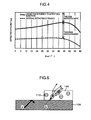
- Fig. 4 is a graph showing a relationship of the efficiency of extraction of light to the output-side substrate 108 and the external extraction efficiency with respect to the angle ⁇ cof (°) in the structure of Fig. 1 .
- the ⁇ cof value so that it is greater than or equal to 35° and less than or equal to 50° (i.e., 35° ⁇ cof ⁇ 50°)
- This ensures that it is possible to reduce the thin-film waveguide mode.
- setting ⁇ cof to ranging from 41° to 46° makes it possible to reduce the thin-film waveguide mode. From the foregoing, it is apparent that appropriate interference condition setup enables reduction of the thin-film waveguide mode.
- Fig. 5 is a diagram for explanation of the principle of the thick-film waveguide mode reduction by means of the light scattering layer 109.
- the light scattering layer 109 is absent, the light having its incidence angle larger than a critical angle of total reflection which is defined by the refractive index of the output-side substrate 108 and the refractive index of ambient air behaves to perform total reflection at an interface between the output-side substrate 108 and the air as indicated by a light ray path "a" in Fig. 5 . This would result in an increase in thick-film waveguide mode.
- fine particles 110 are dispersed in the light scattering layer 109.
- the light Upon incidence of light to such fine particles 110, the light is separated and divided by the scattering phenomena into those light rays traveling in various directions as indicated by a light path b. This results in production of light having its incidence angle smaller than the critical angle of total reflection at the interface between the output-side substrate 108 and the air, thereby making it possible to bring out the light toward the exterior, thus enabling reduction of the thick-film waveguide mode.
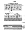
- the particle pitch is a distance between neighboring ones of the fine particles 110 in a direction along the layer plane as shown in Fig. 6 .
- the average particle pitch is an average value of pitch values of those of all the fine particles 110 within a square surface region of the light scattering layer 109 with an area of 20 ⁇ m by 20 ⁇ m.
- the height, 98 nm, of the luminous point 104 from the reflection electrode 102 is the value in the case of ⁇ cof being set to 42°.
- the grain size of a particle 110 may be thought as the average grain size.
- Figs. 7 and 8 show simulation results in the case of the refractive index of fine particles 110 being set at 2.4 and 1.8, respectively. It is noted that a thick-film waveguide mode in the case of the light scattering layer 109 being absent is indicated so that the average particle pitch is 0 ⁇ m for purposes of convenience in discussion herein. Also indicated in the graphs are thick-film waveguide modes which are estimated from light amount measurement results of OLEDs that were fabricated by using as the fine particles 110 of light scattering layer 109 those fine particles 110 of zirconium oxide having a refractive index 2.4 at a refractive index 2.4, a grain size of 0.57 ⁇ m and grain size of 1.0 ⁇ m, respectively.
- the thick-film waveguide mode was reduced within a particle grain size range of from 0.5 ⁇ m to 6.0 ⁇ m and within an average particle pitch range of 0.5 ⁇ m to 12 ⁇ m. More preferably, the thick-film waveguide mode was reduced more successfully within a particle grain size range of 0.5 ⁇ m to 4.0 ⁇ m and within an average particle pitch range of 0.5 ⁇ m to 7.0 ⁇ m.
- the average particle pitch is preferably set so that it ranges from 0.5 ⁇ m to 3.0 ⁇ m whereas an optimal value of the average particle pitch is 1.0 ⁇ m.
- the average particle pitch is preferably set at 1.0 time to 6.0 times the grain size of particles 110; in particular, the best possible value of it is 2.0 times.
- the average particle pitch is preferably set to ranging from 1.0 ⁇ m to 3.5 ⁇ m; an optimum value of the average particle pitch is 3.0 ⁇ m.
- the average particle pitch is preferably set at 1.0 to 3.5 times the grain size of particles 110; in particular, the best value of it is 3.0 times.
- the average particle pitch is preferably set to ranging from 2.0 ⁇ m to 4.75 ⁇ m; an optimum value of the average particle pitch is 4.0 ⁇ m.
- the average particle pitch is preferably set at 1.0 to 2.4 times the grain size of particles 110; in particular, the best value is 2.0 times.
- the average particle pitch is preferably set to ranging from 4.0 ⁇ m to 7.0 ⁇ m; an optimum value of the average particle pitch is 6 ⁇ m.
- the average particle pitch is preferably set at 1.0 to 1.8 times the grain size of particles 110; in particular, the best value is 1.50 times.
- the thick-film waveguide mode is reduced within a particle grain size range of from 0.5 ⁇ m to 6.0 ⁇ m and within an average particle pitch range of 0. 5 ⁇ m to 12 ⁇ m. More preferably, the thick-film waveguide mode is reduced more successfully within a particle grain size range of 0.5 ⁇ m to 2.0 ⁇ m and within an average particle pitch range of 0.5 ⁇ m to 4.0 ⁇ m.
- the average particle pitch falls within a range of from 0.5 ⁇ m to 2.75 ⁇ m.
- An optimal value of the average particle pitch is 1.50 ⁇ m.
- the average particle pitch is preferably set at 1.0 time to 5.5 times the grain size of particles 110; in particular, the best possible value thereof is 3.0 times.
- the average particle pitch ranges from 1.0 ⁇ m to 3.25 ⁇ m; an optimum value of the average particle pitch is 1.5 ⁇ m.
- the average particle pitch is preferably set at 1.0 to 3.3 times the grain size of particles 110; in particular, the best value is 1.5 times.
- the average particle pitch ranges from 2.0 ⁇ m to 4.0 ⁇ m; an optimum value of the average particle pitch is 2.0 ⁇ m.
- the average particle pitch is preferably set at 1.0 to 2.0 times the grain size of particles 110; in particular, the best value is 1.0 time.
- the fine particles 110 may contain therein those particles 110 with grain sizes smaller than 0.5 ⁇ m or other particles 110 with grain sizes larger than 6.0 ⁇ m.
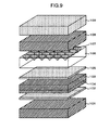
- FIG. 9 An exploded perspective view of such structure capable of reducing the thin-film waveguide mode is shown in Fig. 9 ; a cross-sectional view thereof is shown in Fig. 10 .
- An ensemble of first conic solid-like transparent resin bodies 107 is buried or embedded in a first transparent resin layer 106 in such a manner that each conic resin has its bottom face adhered to a surface of an output-side substrate 108.
- the first conic solid-like transparent resin 107 has its refractive index which is settable to any value falling within a range of from 1.4 to 1.8.
- the first conic solid-like transparent resin 107 has an increasing expanse from the first transparent resin layer 106 toward the output-side substrate 108.
- a spread angle of the first conic solid-like transparent resin 107 in the direction toward the output-side substrate 108 is represented by ⁇ pri as shown in Fig. 10 .
- the refractive index of the first conic solid-like transparent resin 107 is denoted by npri; the refractive index of transparent resin is given as nLPL.
- Fig. 11 is a principle diagram of thin-film waveguide mode reduction in this embodiment.
- the refractive index of first conic solid-like transparent resin 107 is smaller than the refractive index of first transparent resin layer 106 and, simultaneously, greater than or equal to the refractive index of output-side substrate 108.
- the first conic solid-like transparent resin 107 having a circular cone shape is not provided, light had experienced total reflection at an interface between the first transparent resin layer 106 and the output-side substrate 108 along a light path shown by "a" in Fig. 11 .
- a light path is formed as shown by "b" in Fig. 11 . More specifically, the angle of incidence of light from the first transparent resin layer 106 into the first conic solid-like transparent resin 107 becomes less than the incidence angle of light from the first transparent resin layer 106 to the output-side substrate 108 as shown by "a” in Fig. 11 whereby total reflection does not take place so that the light goes out into the output-side substrate 108. This makes it possible to reduce the thin-film waveguide mode.
- the light path b in Fig. 11 is indicated in an exemplary case where the first conic solid-like transparent resin 107 is the same in refractive index as the output-side substrate 108.
- Fig. 12 shows simulation results of a relationship of ⁇ pri and relative value of thin-film waveguide mode under various interference conditions while using the following setup values: 460 nm for the light wavelength, 150 nm for the film thickness of organic layer 103, 1.6 for the refractive index of first transparent resin layer 106, and 1.5 for the refractive index of first conic solid-like transparent resin 107 of the circular cone shape type.
- the relative value of the thin-film waveguide mode exhibits strong dependency upon ⁇ cof and ⁇ pri.
- the distance a ⁇ d up to the center of luminous point 104 corresponding to the ⁇ cof range of from 36° to 48° is given as: (2-155/180) ⁇ /4/n/cos36° ⁇ a ⁇ d ⁇ (2-155/180) ⁇ /4/n/cos48°. That is, the distance is more than or equal to 90 nm and less than or equal to 109 nm.
- Fig. 13 shows simulation results of the relationship of ⁇ pri and relative value of thin-film waveguide mode under various interference conditions while setting the light's wavelength to 460 nm, the film thickness of organic layer 103 to 150 nm, the refractive index of first transparent resin layer 106 at 1.7, and the refractive index of first conic solid-like transparent resin 107 at 1.5.
- Fig. 14 shows simulation results of the relationship of ⁇ pri and relative value of thin-film waveguide mode under various interference conditions while setting the light's wavelength to 460 nm, the film thickness of organic layer 103 to 150 nm, the refractive index of first transparent resin layer 106 at 1.7, and the refractive index of first conic solid-like transparent resin 107 at 1.6.
- Fig. 15 shows simulation results of the relationship of ⁇ pri and relative value of thin-film waveguide mode under various interference conditions while setting the light wavelength to 460 nm, the film thickness of organic layer 103 to 150 nm, the refractive index of first transparent resin layer 106 at 1.8, and the refractive index of first conic solid-like transparent resin 107 at 1.5.
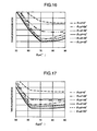
- Fig. 16 shows simulation results of the relationship of ⁇ pri and relative value of thin-film waveguide mode under various interference conditions while setting the light wavelength to 460 nm, the film thickness of organic layer 103 to 150 nm, the refractive index of first transparent resin layer 106 at 1.8, and the refractive index of first conic solid-like transparent resin 107 at 1.6.
- Fig. 17 shows simulation results of the relationship of ⁇ pri and relative value of thin-film waveguide mode under various interference conditions while setting the light wavelength to 460 nm, the film thickness of organic layer 103 to 150 nm, the refractive index of first transparent resin layer 106 at 1.8, and the refractive index of first conic solid-like transparent resin 107 at 1.7.
- Fig. 18 shows simulation results of the relationship of ⁇ pri and relative value of thin-film waveguide mode under various interference conditions while setting the light wavelength to 460 nm, the film thickness of organic layer 103 to 150 nm, the refractive index of first transparent resin layer 106 at 1.9, and the refractive index of first conic solid-like transparent resin 107 at 1.5.
- Fig. 19 shows simulation results of the relationship of ⁇ pri and relative value of thin-film waveguide mode under various interference conditions while setting the light wavelength to 460 nm, the film thickness of organic layer 103 to 150 nm, the refractive index of first transparent resin layer 106 at 1.9, and the refractive index of first conic solid-like transparent resin 107 at 1.6.
- Fig. 20 shows simulation results of the relationship of ⁇ pri and relative value of thin-film waveguide mode under various interference conditions while setting the light wavelength to 460 nm, the film thickness of organic layer 103 to 150 nm, the refractive index of first transparent resin layer 106 at 1.9, and the refractive index of first conic solid-like transparent resin 107 at 1.7.
- Fig. 21 shows simulation results of the relationship of ⁇ pri and relative value of thin-film waveguide mode under various interference conditions while setting the light wavelength to 460 nm, the film thickness of organic layer 103 to 150 nm, the refractive index of first transparent resin layer 106 at 1.9, and the refractive index of first conic solid-like transparent resin 107 at 1.8.
- Fig. 22 shows simulation results of the relationship of ⁇ pri and relative value of thin-film waveguide mode under various interference conditions while setting the light wavelength to 460 nm, the film thickness of organic layer 103 to 150 nm, the refractive index of first transparent resin layer 106 at 2.0, and the refractive index of first conic solid-like transparent resin 107 at 1.5.
- Fig. 23 shows simulation results of the relationship of ⁇ pri and relative value of thin-film waveguide mode under various interference conditions while setting the light wavelength to 460 nm, the film thickness of organic layer 103 to 150 nm, the refractive index of first transparent resin layer 106 at 2.0, and the refractive index of first conic solid-like transparent resin 107 at 1.6.
- Fig. 24 shows simulation results of the relationship of ⁇ pri and relative value of thin-film waveguide mode under various interference conditions while setting the light wavelength to 460 nm, the film thickness of organic layer 103 to 150 nm, the refractive index of first transparent resin layer 106 at 2.0, and the refractive index of first conic solid-like transparent resin 107 at 1.7.
- Fig. 25 shows simulation results of the relationship of ⁇ pri and relative value of thin-film waveguide mode under various interference conditions while setting the light wavelength to 460 nm, the film thickness of organic layer 103 to 150 nm, the refractive index of first transparent resin layer 106 at 2.0, and the refractive index of first conic solid-like transparent resin 107 at 1.8.
- Fig. 26 is a graph showing a relation of thin-film waveguide mode plotted in vertical axis versus refractive index nLPL of first transparent resin layer 106 plotted in transverse axis while letting respective values of the refractive index npri (1.4, 1.5, 1.6, 1.7 and 1.8) of first conic solid-like transparent resin 107 in case ⁇ cof and ⁇ pri are optimized (i.e., these are set in the condition that the thin-film waveguide mode becomes the lowest value).
- the refractive index nLPL of first transparent resin layer 106 is set to ranging from 1.7 to 2.0 (i.e., 1.7 ⁇ nLPL ⁇ 2.0).
- the refractive index of first conic solid-like transparent resin 107 is set to larger than or equal to 1.5 and less than 1.7 (1.5 ⁇ nLPL ⁇ 1.7).
- the relationship of these refractive indexes and thin-film waveguide mode is closely related to respective refractive index ratios of the first transparent resin layer 106, first conic solid-like transparent resin 107 and output-side substrate 108. For example, it becomes easier for light to enter the first conic solid-like transparent resin bodies 107 from first transparent resin layer 106 when the refractive index of first conic solid-like transparent resin 107 becomes higher in value; adversely, it becomes difficult for the light to enter the output-side substrate 108 from first conic solid-like transparent resin 107.
- the ratio, nLPL/nglass, of the refractive index of first transparent resin layer 106 to the refractive index of output-side substrate 108 is set to ranging from 1.13 to 1.33, where nLPL is the refractive index of first transparent resin layer 106, and nglass is the refractive index of output-side substrate 108. It is also recommended that the ratio, npri/nglass, of the refractive index of first conic solid-like transparent resin 107 to the refractive index of output-side substrate 108 is set to ranging from 1 to 1.13.
- refractive indexes have been stated using discrete values with a resolution of 0.1, refractive indexes of actual members are continuous values; so, the above-stated refractive index values are expressed by approximate values, each of which is obtained by rounding the refractive index of an actual member at the second decimal place. Rounding refractive indexes results in no appreciable variation in the above-stated preferable essential factors for reducing the thin-film waveguide mode, such as the angle range of ⁇ pri, etc.
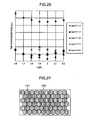
- Fig. 27 is a plan view of a surface of the first transparent resin layer 106 on the output-side substrate 108 side.
- the circular cone-shaped bodies of the first conic solid-like transparent resin 107 are disposed in a densely filling layout as shown in Fig. 27 . With this dense fill layout, gaps among neighboring cones of the first conic solid-like transparent resin 107 become smaller in size, thus enabling achievement of further reduction of the thin-film waveguide mode.
- the first conic solid-like transparent resin 107 is not limited to the one of the circular cone type shown in Fig. 9 , and may be arranged to have either a quadrangular pyramid-like shape shown in Fig. 28 or a six-sided pyramid shape shown in Fig. 29 . Note however that it is desirable to arrange the shape of first conic solid-like transparent resin 107 to have the circular conic shape. This can be said because the thin-film waveguide mode is reducible in all inplane directions of the OLED device.
- the thick-film waveguide mode it is possible to reduce the thick-film waveguide mode by appropriate setup of the grain size and the layout density of the fine particles 110 of the light scattering layer 109. It is also possible to reduce the thin-film waveguide mode by appropriately performing setup of the luminous point 104 or, alternatively, setup of both the refraction index of first transparent resin layer 106 and the refractive index and spreading angle of first conic solid-like transparent resin 107 in addition to the setup of the luminous point 104. With the schemes stated above, highly enhanced light extraction efficiency is obtainable in the OLED of this embodiment. Additionally, with the above-noted arrangement, color mixture is accelerated in cases where two or more luminous layers having different colors are multilayered.
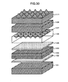
- Fig. 30 is an exploded perspective view of an organic light emitting diode (OLED) in accordance with this embodiment.
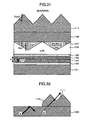
- Fig. 31 is a cross-sectional view of the OLED of this embodiment.
- the OLED of this embodiment has a reflection-side substrate 101, aluminum reflection electrode 102, organic layer 103, transparent electrode 105, first transparent resin layer 106, first conic solid-like transparent resin bodies 107, output-side substrate 108 and second conic solid-like transparent resin 111.
- Figs. 30-31 are for explanation of the top-emission type, the bottom-emission type may alternatively be employable.
- the organic layer 103 composed of organic molecules is formed on the aluminum reflection electrode 102 which is formed on the reflection-side substrate 101.
- the organic layer 103 includes a luminous point 104. From this luminous point 104, blue light emission with a peak wavelength of 460 nm takes place. On the organic layer 103, the transparent electrode 105 is formed. On this transparent electrode 105, the first transparent resin layer 106 is disposed. The first transparent resin layer 106 has its top surface in which are embedded the first conic solid-like transparent resin bodies 107 each having a bottom face adhered to a surface of the output-side substrate 108.
- the first conic solid-like transparent resin 107 of the circular cone shape has a refractive index of about 1.5.
- the output-side substrate 108 is situated on the first transparent resin layer 106.
- the first conic solid-like transparent resin 107 has expanse toward the output-side substrate 108 from the first transparent resin layer 106 in a normal line direction of the output-side substrate 108.
- the OLED also has the second conic solid-like transparent resin 111 on the output-side substrate 108.
- the second conic solid-like transparent resin 111 is constituted from a resin layer of rectangular parallelepiped and a plurality of circular cone-shaped resin bodies disposed thereon, the rectangular resin layer is not always required.
- the second conic solid-like transparent resin 111 has its bottom face which is adhered to an air-side surface of the output-side substrate 108.
- the second conic solid-like transparent resin 111 is fabricated by molding an acrylate resin.
- the refractive index of such acrylate resin is about 1.5, which is the same as the refractive index of the output-side substrate 108.
- the second conic solid-like transparent resin 111 has expanse from ambient air toward the output-side substrate 108 (in the opposite direction to the direction of light extraction from the organic layer 103). Note here that in this description, the expansion angle of the second conic solid-like transparent resin 111 in the direction toward the output-side substrate 108 is represented by ⁇ pri2 as shown in Fig. 31 .
- a thin-film waveguide reduction technique mode of this embodiment is similar to the scheme that has been indicated in the embodiment 1 stated supra.
- Fig. 32 is a diagram for explanation of the principle of the thick-film waveguide mode reduction in this embodiment.
- the second conic solid-like transparent resin 111 In a case where the second conic solid-like transparent resin 111 is not provided, light having its incident angle larger than the total reflection critical angle at an interface between the output-side substrate 108 and the air behaves to perform total reflection at the interface between output-side substrate 108 and air as indicated by a light path "a" in Fig. 32 . This results in an increase in thick-film waveguide mode.
- the incident angle becomes smaller due to the inclination of the second conic solid-like transparent resin 111 as indicated by a light path "b" in Fig. 32 , resulting in extraction of the light to the exterior, thereby enabling reduction of the thick-film waveguide mode.
- the refractive index nLPL of first transparent resin layer 106 was set to several values, such as 1.6, 1.7, 1.8, 1.9 and 2.0, whereas ⁇ pri1 of first conic solid-like transparent resin 107 was at 80°, 80°, 75°, 79° and 76°, respectively.
- the second conic solid-like transparent resin 111 may be designed to have any one of the circular conic shape, the pyramid-like shape and the six-sided pyramid shape. By employing a dense fill layout, it is possible to enhance the efficiency more significantly for the same reason as that described concerning the layout of the first transparent resin layer 106 in the embodiment 1.
- Fig. 34 is an exploded perspective view of an organic light emitting diode (OLED) of this embodiment.
- Fig. 35 is a cross-sectional view of the OLED of this embodiment.
- the OLED of this embodiment has a reflection-side substrate 101, aluminum reflection electrode 102, organic layer 103, transparent electrode 105, first transparent resin layer 106, diffuse reflection layer 112, second transparent resin layer 113 and output-side substrate 108.
- Figs. 34-35 are explanation diagrams of the top-emission type OLED, the bottom-emission type may alternatively be employed.
- the organic layer 103 composed of organic molecules is formed on the reflection-side substrate 101.
- the organic layer 103 involves a luminous point 104.
- the transparent electrode 105 is formed on the organic layer 103.
- the first transparent resin layer 106 is disposed.
- the diffuse reflection layer 112 is adhered by the first transparent resin layer 106.
- the diffuse reflection layer 112 has openings at those areas in which the reflection electrode 102 and transparent electrode 105 overlap each other in the normal line direction of the diffuse reflection layer 112. More specifically, in a case where one of the reflection electrode 102 and transparent electrode 105 is formed to have a solid plate shape whereas the other has a stripe shape, the openings of the diffuse reflection layer 112 become to have a stripe shape. Alternatively, in case both of the reflection electrode 102 and transparent electrode 105 have stripe shapes whose extension directions are at right angles to each other, the openings of the diffuse reflection layer 112 become a dot-like shape as shown in Fig. 34 . This dot shape is desirable for the openings of the diffuse reflection layer 112.
- the diffuse reflection layer 112 may typically be a white sheet with high reflectivity.
- An example of the white sheet is a polyethylene terephthalate (PET) film containing therein a great number of fine air bubbles created by foaming processes.
- PET polyethylene terephthalate
- a practical example of it is Lumirror E60L, E6SL or E60V, which is a foam polyester film manufactured by Toray Industries, Inc..
- the white sheet material include, but not limited to, a white resin/powder mixture which is composed of either an acrylate resin with its lateral chain carbon number of 4 or more or an acrylic resin with its side chain carbon number ranging from 1 to 3 and with a plasticizer, such as dibutyl phthalate (DBP) or the like, being added thereto, while causing the resin to contain therein a white powder of magnesium oxide, titanium oxide, barium titanate or else.
- a white rubber/powder mixture which is composed of chloroprene rubber, silicon rubber or fluorine-based rubber which contains a white powder of magnesium oxide, titanium oxide, barium titanate or else.
- a further example is a metallic reflective film having on its surface a fine concavo-convex configuration, such as that used as the diffuse reflection layer 112 of a reflection-type liquid crystal display (LCD) apparatus.
- a surface of the second transparent resin layer 113 on the output-side substrate 108 side is processed to have such concavoconvex shape; then, a film of high-reflective-index metal, such as aluminum or silver, is fabricated thereon by sputtering methods.
- the second transparent resin layer 113 covers the diffuse reflection layer 112; so, the second transparent resin layer 113 is contained in the openings of the diffuse reflection layer 112.
- the output-side substrate 108 is adhered by the second transparent resin layer 113.
- the second transparent resin layer 113 is made of acrylic resin similar to that of the first transparent resin layer 106. Also note that the second transparent resin layer 113 may not necessarily be the same as the first transparent resin layer 106. But, by letting the material of the second transparent resin layer 113 be the same as that of the first transparent resin layer 106, the refractive indexes of these layers become the same as each other, resulting in the interfaces of the first transparent resin layer 106 and second transparent resin layer 113 becoming optically continuous. In other words, it becomes optically equivalent to the case where the interfaces of the first transparent resin layer 106 and second transparent resin layer 113 are absent.
- Fig. 36 is a diagram for explanation of the principle of the thick-film waveguide mode reduction in this embodiment.
- the light that experienced total reflection at the interface between the output-side substrate 108 and ambient air performs diffuse reflection at the diffuse reflection layer 112.
- An incident angle at the interface between output-side substrate 108 and air of a part of the light that diffused and reflected in the diffuse reflection layer 112 becomes smaller than the total reflection critical angle; thus, the light is taken out or "released" to the air side.
- the diffuse reflection layer 112 it has been difficult to release the light toward the air side because the light repeats total reflection with almost the same incident angle at the interface between the output-side substrate 108 and air and also at the reflection electrode 102.
- the thin-film waveguide mode reduction in this embodiment is achieved by setting interference conditions appropriately.
- ⁇ cof By setting ⁇ cof to ranging from about 35° to 50° in a similar way to that of the embodiment 1 shown in Fig. 4 , it is possible to reduce the thin-film waveguide mode.
- a further preferable device structure may be arranged by embedding the first conic solid-like transparent resin 107 used in the embodiment 1 in the first transparent resin layer 106.
- the refractive index of first transparent resin layer 106, ⁇ cof, ⁇ pri and refractive index of first conic solid-like transparent resin 107 similar arrangements to those stated in the embodiment 1 are applicable. Note however that in this embodiment, the bottom face of the first conic solid-like transparent resin 107 is bonded by the diffuse reflection layer 112 to second transparent resin layer 113.
Landscapes
- Physics & Mathematics (AREA)
- Optics & Photonics (AREA)
- Electroluminescent Light Sources (AREA)
- Optical Elements Other Than Lenses (AREA)
Applications Claiming Priority (1)
| Application Number | Priority Date | Filing Date | Title |
|---|---|---|---|
| JP2010111609A JP5216806B2 (ja) | 2010-05-14 | 2010-05-14 | 有機発光ダイオード及びこれを用いた光源装置 |
Publications (1)
| Publication Number | Publication Date |
|---|---|
| EP2387085A1 true EP2387085A1 (de) | 2011-11-16 |
Family
ID=44510574
Family Applications (1)
| Application Number | Title | Priority Date | Filing Date |
|---|---|---|---|
| EP11164715A Withdrawn EP2387085A1 (de) | 2010-05-14 | 2011-05-04 | Organische lichtemittierende Diode und Lichtquellenvorrichtung damit |
Country Status (3)
| Country | Link |
|---|---|
| US (1) | US20110278557A1 (de) |
| EP (1) | EP2387085A1 (de) |
| JP (1) | JP5216806B2 (de) |
Families Citing this family (10)
| Publication number | Priority date | Publication date | Assignee | Title |
|---|---|---|---|---|
| TW516164B (en) * | 2000-04-21 | 2003-01-01 | Semiconductor Energy Lab | Self-light emitting device and electrical appliance using the same |
| US8764504B2 (en) * | 2011-02-25 | 2014-07-01 | Semiconductor Energy Laboratory Co., Ltd. | Lighting device and method for manufacturing the same |
| DE102011076750A1 (de) * | 2011-05-31 | 2012-12-06 | Osram Opto Semiconductors Gmbh | Optoelektronisches Bauelement und Verfahren zum Herstellen eines optoelektronischen Bauelements |
| JP2013191314A (ja) * | 2012-03-12 | 2013-09-26 | Idemitsu Kosan Co Ltd | 有機エレクトロルミネッセンス素子 |
| JP5938363B2 (ja) * | 2013-03-25 | 2016-06-22 | 富士フイルム株式会社 | 有機電界発光素子 |
| WO2014185224A1 (ja) * | 2013-05-17 | 2014-11-20 | 旭硝子株式会社 | 有機led素子、有機led素子の製造方法 |
| KR101859303B1 (ko) * | 2013-06-12 | 2018-06-28 | 미쯔비시 케미컬 주식회사 | El용 광 취출 필름, el용 광 취출 필름의 제조 방법 및 면 발광체 |
| WO2015029203A1 (ja) * | 2013-08-30 | 2015-03-05 | 株式会社日立製作所 | 有機発光装置 |
| JP6437752B2 (ja) * | 2014-07-25 | 2018-12-12 | 京セラ株式会社 | インクジェットヘッド及びインクジェットプリンタ |
| CN105280838B (zh) * | 2015-09-22 | 2017-08-25 | 深圳市华星光电技术有限公司 | 一种oled发光器件及显示装置 |
Citations (5)
| Publication number | Priority date | Publication date | Assignee | Title |
|---|---|---|---|---|
| JP2003086353A (ja) * | 2001-09-11 | 2003-03-20 | Nissan Chem Ind Ltd | 有機el素子用透明性基板および有機el素子 |
| JP2004296423A (ja) | 2002-11-26 | 2004-10-21 | Nitto Denko Corp | 有機エレクトロルミネッセンス素子、面光源および表示装置 |
| EP1548856A2 (de) * | 2003-12-26 | 2005-06-29 | Nitto Denko Corporation | Elektrolumineszierende Vorrichtung, planare Lichtquelle und Anzeigevorrichtung |
| US20090051276A1 (en) * | 2007-08-21 | 2009-02-26 | Katsumi Inoue | Organic electroluminescent display |
| WO2009028620A1 (ja) * | 2007-08-28 | 2009-03-05 | Panasonic Electric Works Co., Ltd. | 有機エレクトロルミネッセンス素子 |
Family Cites Families (4)
| Publication number | Priority date | Publication date | Assignee | Title |
|---|---|---|---|---|
| JP4495978B2 (ja) * | 2003-03-07 | 2010-07-07 | 日東電工株式会社 | 有機エレクトロルミネッセンス素子とこの素子を用いた面光源および表示装置 |
| US20040217702A1 (en) * | 2003-05-02 | 2004-11-04 | Garner Sean M. | Light extraction designs for organic light emitting diodes |
| WO2009017035A1 (ja) * | 2007-07-27 | 2009-02-05 | Asahi Glass Co., Ltd. | 透光性基板、その製造方法、有機led素子及びその製造方法 |
| JP2009266449A (ja) * | 2008-04-23 | 2009-11-12 | Rohm Co Ltd | 有機el素子 |
-
2010
- 2010-05-14 JP JP2010111609A patent/JP5216806B2/ja not_active Expired - Fee Related
-
2011
- 2011-05-04 EP EP11164715A patent/EP2387085A1/de not_active Withdrawn
- 2011-05-05 US US13/101,218 patent/US20110278557A1/en not_active Abandoned
Patent Citations (6)
| Publication number | Priority date | Publication date | Assignee | Title |
|---|---|---|---|---|
| JP2003086353A (ja) * | 2001-09-11 | 2003-03-20 | Nissan Chem Ind Ltd | 有機el素子用透明性基板および有機el素子 |
| JP2004296423A (ja) | 2002-11-26 | 2004-10-21 | Nitto Denko Corp | 有機エレクトロルミネッセンス素子、面光源および表示装置 |
| EP1548856A2 (de) * | 2003-12-26 | 2005-06-29 | Nitto Denko Corporation | Elektrolumineszierende Vorrichtung, planare Lichtquelle und Anzeigevorrichtung |
| US20090051276A1 (en) * | 2007-08-21 | 2009-02-26 | Katsumi Inoue | Organic electroluminescent display |
| WO2009028620A1 (ja) * | 2007-08-28 | 2009-03-05 | Panasonic Electric Works Co., Ltd. | 有機エレクトロルミネッセンス素子 |
| EP2190265A1 (de) * | 2007-08-28 | 2010-05-26 | Panasonic Electric Works Co., Ltd | Organische elektrolumineszenzvorrichtung |
Also Published As
| Publication number | Publication date |
|---|---|
| US20110278557A1 (en) | 2011-11-17 |
| JP5216806B2 (ja) | 2013-06-19 |
| JP2011243290A (ja) | 2011-12-01 |
Similar Documents
| Publication | Publication Date | Title |
|---|---|---|
| US20110278557A1 (en) | Organic light emitting diode and light source device including the same | |
| CN112397547A (zh) | 显示装置 | |
| US9978821B2 (en) | Display device | |
| US8643259B2 (en) | Optical sheet and surface light source apparatus | |
| KR102755265B1 (ko) | 백라이트 유닛 및 이를 포함하는 표시 장치 | |
| JP2006164808A (ja) | 発光素子,照明装置及びこれを有する表示装置 | |
| US7690829B2 (en) | Surface light emitter and display apparatus | |
| US10367170B2 (en) | Light emitting device with irregularities located on a first light transmissive substrate and a second light transmissive substrate | |
| US11650365B2 (en) | Surface light source | |
| JP2011086527A (ja) | El素子、照明装置及びディスプレイ装置 | |
| JP5803506B2 (ja) | 発光素子及び照明器具 | |
| WO2020024765A1 (zh) | 显示面板及其制造方法、显示装置 | |
| JP5481825B2 (ja) | El素子およびディスプレイ装置 | |
| JP2015176735A (ja) | El素子、照明装置、ディスプレイ装置、および液晶ディスプレイ装置 | |
| JP5560359B2 (ja) | 有機発光ダイオード及びこれを用いた光源装置 | |
| KR102743169B1 (ko) | Oled 디스플레이 패널 및 디스플레이 장치 | |
| JP5862576B2 (ja) | 発光素子 | |
| CN102110779B (zh) | 有机发光装置 | |
| JP4830746B2 (ja) | 照明装置および液晶表示装置 | |
| JP5673295B2 (ja) | 発光素子及び照明器具 | |
| JP6167883B2 (ja) | 面発光ユニット | |
| US20260110827A1 (en) | Electronic device | |
| JP6167884B2 (ja) | 面発光ユニット | |
| CN114975825A (zh) | 显示面板和显示装置 | |
| JP2013077412A (ja) | El素子及びこれを用いた照明装置、ディスプレイ装置、液晶ディスプレイ装置 |
Legal Events
| Date | Code | Title | Description |
|---|---|---|---|
| 17P | Request for examination filed |
Effective date: 20110902 |
|
| AK | Designated contracting states |
Kind code of ref document: A1 Designated state(s): AL AT BE BG CH CY CZ DE DK EE ES FI FR GB GR HR HU IE IS IT LI LT LU LV MC MK MT NL NO PL PT RO RS SE SI SK SM TR |
|
| AX | Request for extension of the european patent |
Extension state: BA ME |
|
| PUAI | Public reference made under article 153(3) epc to a published international application that has entered the european phase |
Free format text: ORIGINAL CODE: 0009012 |
|
| STAA | Information on the status of an ep patent application or granted ep patent |
Free format text: STATUS: EXAMINATION IS IN PROGRESS |
|
| 17Q | First examination report despatched |
Effective date: 20170302 |
|
| STAA | Information on the status of an ep patent application or granted ep patent |
Free format text: STATUS: THE APPLICATION IS DEEMED TO BE WITHDRAWN |
|
| 18D | Application deemed to be withdrawn |
Effective date: 20200228 |