EP2390702A1 - Module de caméra et son procédé de fabrication - Google Patents
Module de caméra et son procédé de fabrication Download PDFInfo
- Publication number
- EP2390702A1 EP2390702A1 EP10014209A EP10014209A EP2390702A1 EP 2390702 A1 EP2390702 A1 EP 2390702A1 EP 10014209 A EP10014209 A EP 10014209A EP 10014209 A EP10014209 A EP 10014209A EP 2390702 A1 EP2390702 A1 EP 2390702A1
- Authority
- EP
- European Patent Office
- Prior art keywords
- lens set
- dry film
- film type
- type photoresist
- spacer
- Prior art date
- Legal status (The legal status is an assumption and is not a legal conclusion. Google has not performed a legal analysis and makes no representation as to the accuracy of the status listed.)
- Ceased
Links
Images




Classifications
-
- G—PHYSICS
- G02—OPTICS
- G02B—OPTICAL ELEMENTS, SYSTEMS OR APPARATUS
- G02B13/00—Optical objectives specially designed for the purposes specified below
- G02B13/001—Miniaturised objectives for electronic devices, e.g. portable telephones, webcams, PDAs, small digital cameras
- G02B13/0085—Miniaturised objectives for electronic devices, e.g. portable telephones, webcams, PDAs, small digital cameras employing wafer level optics
-
- H—ELECTRICITY
- H10—SEMICONDUCTOR DEVICES; ELECTRIC SOLID-STATE DEVICES NOT OTHERWISE PROVIDED FOR
- H10F—INORGANIC SEMICONDUCTOR DEVICES SENSITIVE TO INFRARED RADIATION, LIGHT, ELECTROMAGNETIC RADIATION OF SHORTER WAVELENGTH OR CORPUSCULAR RADIATION
- H10F39/00—Integrated devices, or assemblies of multiple devices, comprising at least one element covered by group H10F30/00, e.g. radiation detectors comprising photodiode arrays
- H10F39/80—Constructional details of image sensors
- H10F39/804—Containers or encapsulations
-
- H—ELECTRICITY
- H10—SEMICONDUCTOR DEVICES; ELECTRIC SOLID-STATE DEVICES NOT OTHERWISE PROVIDED FOR
- H10F—INORGANIC SEMICONDUCTOR DEVICES SENSITIVE TO INFRARED RADIATION, LIGHT, ELECTROMAGNETIC RADIATION OF SHORTER WAVELENGTH OR CORPUSCULAR RADIATION
- H10F77/00—Constructional details of devices covered by this subclass
- H10F77/40—Optical elements or arrangements
- H10F77/413—Optical elements or arrangements directly associated or integrated with the devices, e.g. back reflectors
Definitions
- the invention relates to image sensor technology and more particularly to a camera module using photosensitive-type spacers.
- Charge coupled devices (CCD) and complementary metal oxide semiconductor (CMOS) image sensor devices are widely used in digital imaging applications.
- Image capture technology is well known to consumers due to the proliferation of devices employing camera modules, including digital cameras, digital video recorders, image capture capable mobile phones, monitors, and other camera-equipped products.
- a conventional camera module includes an image sensor device (i.e. an image pickup or capturing device) and one or more lens set(s).
- the lens sets are disposed on the image sensor device and arranged in a stack so as to map the image of incident light rays onto the image sensor device.
- Glass spacers are typically disposed between the lens sets and between the image sensor device and the adjacent lens set by adherence, using adhesive materials (i.e. ultra-violet (UV) curing resin or thermo-hardening resin), wherein predetermined distances are maintained between the lens sets and between the image sensor device and the adjacent lens set, to obtain a desired focal distance from the lens sets to the image sensor device.
- adhesive materials i.e. ultra-violet (UV) curing resin or thermo-hardening resin
- Such a focal distance is varied with the lens set(s) design including the number and shapes of the lenses and the spacer thickness.
- a more complex lens set(s) design may be required, wherein the spacer thickness is reduced, when compared to conventional camera modules.
- the total thickness of glass spacers used in high optical performance camera modules and required adhesive materials thereof plays an important role in limiting the dimension and lens set design flexibility of a high optical performance camera module.
- the thinness of the glass spacer thickness is limited to more than 300 ⁇ m and requirement for adhesive materials add to the thickness of the glass spacer, it is difficult to increase optical performance and reduce dimensions of camera modules.
- An embodiment of a camera module comprises an imager sensor device comprising a microlens array.
- a lens set overlies the imager sensor device.
- a first dry film type photoresist spacer is interposed between the imager sensor device and the lens set, wherein the dry film type photoresist spacer has an opening above the microlens array.
- An embodiment of a method for fabricating a camera module comprises providing a lens set having a first surface and a second surface opposite thereto.
- a dry film type photoresist material is coated on the first surface of the lens set.
- the dry film type photoresist material is patterned by a photolithography process to form a spacer with an opening therein.
- the spacer is adhered onto an imager sensor device, such that the lens set is above the image sensor device, wherein the imager sensor device comprises a microlens array under the opening.
- FIGS. 1A to 1C are cross sections of an exemplary embodiment of a method for forming a lens set structure according to the invention
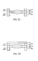
- FIGS. 2A to 2D are cross sections of another exemplary embodiment of a method for forming a lens set structure according to the invention.
- FIG. 3 is a cross section of an exemplary embodiment of a stack lens set structure according to the invention.
- FIG. 4 is a cross section of another exemplary embodiment of a stack lens set structure according to the invention.
- FIGS. 5A to 5D are cross sections of various embodiments of a camera module according to the invention.
- the camera module comprises an imager sensor device 300 comprising a microlens array 302, a lens set 10 is disposed overlying the imager sensor device 300, and a dry film type photoresist spacer 112 interposed between the imager sensor device 300 and the lens set 10.
- the imager sensor device 300 such as an image pickup or capturing device that is also referred to as a solid-state image sensor (SSIS), may be a CCD or CMOS image sensor.
- the lens set 10 is disposed overlying the imager sensor device 300 through the dry film type photoresist spacer 112.
- the lens set 10 may comprise at least one lens element which is formed of a convex or concave lens.
- the lens set 10 may comprise at least one lens element which is formed of a convex or concave lens, and a lens substrate which is adhered to the lens element.
- the lens set 10 comprises a lens substrate 100, and two convex lens elements 102 and 104 formed on two opposite surfaces (e.g. the top surface and the bottom surface) of the lens substrate 100, respectively.
- the lens set 10 may comprise an organic material of glass, epoxy, acryl, or silicone.
- Dry film type photoresist is a photosensitizing material used in photolithography to form precision patterns and provides excellent conformity that allows lamination for a multilayer configuration with the desired thickness.
- the seamless interfaces between dry film photoresist layers are can be achieved by selecting dry film formulation with superior adhesion and applying proper manufacturing processes.
- the dry film type photoresist spacer 112 is employed, instead of a conventional glass spacer, to serve as a lens set support, such that the lens set 10 is spaced from the underlying image sensor device 300.
- the dry film type photoresist spacer 112 also protects the lens element 102 of the lens set 10 from damage.
- the dry film type photoresist spacer 112 has a predetermined thickness to maintain a proper distance between the lens set 10 and the image sensor device 300.
- the predetermined thickness of the dry film type photoresist spacer 112 is based on the desired focal distance from the lens set 10 to the image sensor device 300. For example, the predetermined thickness of the dry film type photoresist spacer 112 is less than 300 ⁇ m and greater than 30 ⁇ m.
- the dry film type photoresist spacer 112 is in direct contact with the lens set 10 and the image sensor 300.
- the dry film type photoresist spacer 112 has an opening 112a above the microlens array 302 of the image sensor device 300.
- a lens set 20 is disposed overlying the lens set 10.
- the lens set 20 may comprise at least one lens element which is formed of a convex or concave lens.
- the lens set 20 may comprise at least one lens element which is formed of a convex or concave lens, and a lens substrate which is adhered to the lens element.
- the lens set 20 comprises a lens substrate 100, and two convex lens elements 202 and 204 formed on the top surface and the bottom surface of the lens substrate 100, respectively.
- the lens set 20 may comprise a material which is the same as or similar to the lens set 10.
- a dry film type photoresist spacer 206 also serves as a lens set support, such that the lens set 20 is spaced from the underlying lens set 10. Moreover, the dry film type photoresist spacer 206 protects the lens elements 102 and 202 from damage. In the embodiment, the dry film type photoresist spacer 206 also has a predetermined thickness to maintain a proper distance between the lens set 10 and the lens set 20. The predetermined thickness of the dry film type photoresist spacer 206 is based on the desired lens set(s) design.
- the dry film type photoresist spacer 112 has a thickness of less than 300 ⁇ m and greater than 30 ⁇ m, and is in direct contact, without the employment of adhesive materials, with the lens set 10 and the overlying lens set 20.
- the dry film type photoresist spacer 206 has an opening 206a which is substantially aligned with the opening 112a of the dry film type photoresist spacer 112.
- FIG. 5C which illustrates further another exemplary embodiment of a camera module according to the invention. Elements in FIG. 5C that are the same as those in FIG. 5A are labeled with the same reference numbers as in FIG. 5A and are not described again for brevity.
- an additional dry film type photoresist spacer 214 is disposed on the lens set 10 for protection of the uppermost lens element 104.
- a transparent cover substrate 216 such as a glass, quartz, or other transparent substrates, may be optionally disposed above the lens set 10 through the dry film type photoresist spacer 214 to further protect the underlying lens set 10.
- the dry film type photoresist spacer 214 has an opening 214a which is substantially aligned with the opening 112a and is in direct contact with the lens set 10 and the transparent cover substrate 216.
- FIG. 5D which illustrates yet another exemplary embodiment of a camera module according to the invention. Elements in FIG. 5D that are the same as those in FIGS. 5B and 5C are labeled with the same reference numbers as in FIGS. 5B and 5C and are not described again for brevity.
- an additional dry film type photoresist spacer 214 is disposed on the lens set 20 for protection of the uppermost lens element 204.
- a transparent cover substrate 216 may be optionally disposed above the lens set 20 through the dry film type photoresist spacer 214 to further protect the underlying lens set 20.
- the dry film type photoresist spacer 214 has an opening 214a which is substantially aligned with the opening 206a and is in direct contact with the lens set 20 and the transparent cover substrate 216.
- a lens set 10 has a surface 10a and a surface 10b is opposite to the surface 10a.
- the lens set 10 may comprise an organic material of glass, epoxy, acryl, or silicone.
- the lens set 10 may comprise at least one lens element which is formed of a convex or concave lens.
- the lens set 10 may comprise at least one lens element which is formed of a convex or concave lens, and a lens substrate which is adhered to the lens element.
- the lens set 10 comprises a lens substrate 100, and two convex lens elements 102 and 104 formed on two opposite surfaces of the lens substrate 100, respectively. Thereafter, a dry film type photoresist material 106 with a predetermined thickness is coated on the first surface 10a of the lens set 10.
- the dry film type photoresist material 106 may comprise a positive or negative dry film photoresist.
- the dry film type photoresist material 106 comprises a positive dry film photoresist. The thickness of the dry film type photoresist material 106 can be adjusted by repeatedly coating thereof.
- the dry film type photoresist material 106 is patterned by a photolithography process including an exposure and development process.
- an exposure process 110 is performed on the dry film type photoresist material 106 using a mask 108 that includes a spacer pattern 108a and a transmissive region 108b, to form an exposed region 106a therein and entirely cover the underlying lens element 102 of the lens set 10 through the transmissive region 108b of the mask 108.
- the dry film type photoresist spacer 112 has a thickness of less than 300 ⁇ m and greater than 30 ⁇ m.
- a lens set structure including the lens set 10 with the dry film type photoresist spacer 112 (as shown in FIG. 1 C) is disposed above and on an imager sensor device 300 by adhering the dry film type photoresist spacer 112 onto the imager sensor device 300 using a conventional baking process, such as a hot forming process. Thereafter, the dry film type photoresist spacer 112 is in direct contact with the image sensor device 300 and a camera module is completed, in which a microlens array 302 of the imager sensor device 300 is under the opening 112a, as shown in FIG. 5A .
- a lens set 20 has a surface 20a and a surface 20b is opposite to the surface 20a.
- the lens set 20 may comprise the same or similar materials as that of the lens set 10 shown in FIG. 1A .
- the lens set 20 may comprise at least one lens element which is formed of a convex or concave lens.
- the lens set 20 may comprise at least one lens element which is formed of a convex or concave lens, and a lens substrate which is adhered to the lens element.
- the lens set 20 comprises a lens substrate 200, and two convex lens elements 202 and 204 formed on two opposite surfaces of the lens substrate 200, respectively.
- a dry film type photoresist spacer 206 with an opening 206a therein is formed on the surface 20a of the lens set 20 by the same method for forming the dry film type photoresist spacer 112 (as shown in FIGS. 1A to 1C ).
- a dry film type photoresist material 208 with a predetermined thickness is coated on the surface 20b of the lens set 20.
- the dry film type photoresist material 208 may comprise the same or similar materials as that of the dry film type photoresist material 106 (as shown in FIG. 1A ).
- the thickness of the dry film type photoresist material 208 can be adjusted by repeatedly coating the dry film photoresist.
- the dry film type photoresist material 208 is patterned by photolithography.
- an exposure process 212 is performed on the dry film type photoresist material 208 using a mask 210 that includes a spacer pattern 210a and a transmissive region 210b, to form an exposed region 208a therein and entirely cover the underlying lens element 204 of the lens set 20 through the transmissive region 210b of the mask 210.
- a development process is performed to remove the exposed region 208a in the dry film type photoresist material 208 and then the dry film type photoresist spacer 214 with an opening 214a therein is formed in direct contact with the lens set 20, as shown in FIG. 2C .
- the opening 214a is substantially aligned to and opposite to the opening 206a.
- a transparent cover substrate 216 such as a glass, quartz or other transparent substrates, is optionally adhered onto the dry film type photoresist spacer 214 by a conventional baking process, such as a hot forming process, such that the transparent cover substrate 216 is above the lens set 20 through the dry film type photoresist spacer 214 that is in direct contact with the lens set 20.
- a lens set structure including the lens set 10, the dry film type photoresist spacers 112 and 214 and the optional transparent cover substrate 216 may be formed by the same method for forming the lens set structure shown in FIGS. 2A to 2D . Thereafter, the lens set structure including the lens set 10, the dry film type photoresist spacers 112 and 214 and the transparent cover substrate 216 is disposed above and on an imager sensor device 300 by adhering the dry film type photoresist spacer 112 onto the imager sensor device 300 using a conventional baking process, such as a hot forming process. As a result, the dry film type photoresist spacer 112 is in direct contact with the image sensor device 300 and a camera module is completed, as shown in FIG. 5C .
- the stack lens set structure may comprises a lens set 10 with the dry film type photoresist spacer 112 and a lens set 20 with the dry film type photoresist spacer 206 vertically stacked on the lens set 10.
- the stack lens set structure may be formed by repeatedly performing the method shown in FIGS. 1A to 1C and at least one baking process for adhering the dry film type photoresist spacer 206 onto the lens set 10.
- the stack lens set structure may comprise more than two lens sets and may be formed by the same or similar methods as that of forming the stack lens set structure shown in FIG. 3 .
- the dry film type photoresist spacer 112 is in direct contact with the image sensor device 300 and a camera module is completed, as shown in FIG. 5B .
- the stack lens set structure may comprises a lens set 10 with the dry film type photoresist spacer 112 (as shown in FIG. 1C ) and a lens set 20 with the dry film type photoresist spacers 206 and 214 and an optional transparent cover substrate 216 (as shown in FIG. 2D ) vertically stacked on the lens set 10.
- the stack lens set structure may be formed by performing the method shown in FIGS. 1A to 1C , the method shown in FIGS. 2A to 2D and at least one baking process for adhering the dry film type photoresist spacer 206 onto the lens set 10.
- the stack lens set structure may comprise more than two lens sets and may be formed by the same or similar methods as that of forming the stack lens set structure shown in FIG. 4 .
- the stack lens set structure shown in FIG. 4 is further disposed on an imager sensor device 300 by adhering the dry film type photoresist spacer 112 onto the imager sensor device 300 using a conventional baking process, such as a hot forming process. As a result, the dry film type photoresist spacer 112 is in direct contact with the image sensor device 300 and a camera module is completed, as shown in FIG. 5D .
- the camera module shown in FIGS. 5A, 5B , 5C or 5D can be fabricated by a wafer level process.
- an integrated circuit manufacturing process is performed to prepare a wafer, for example, a silicon wafer, having multiple image sensor devices 300 thereon.
- the spacer(s), the lens set(s), and the optional transparent cover substrate for each camera module can be fabricated in manifold on substrates. After stacking the substrates and the wafer having multiple image sensor devices 300, the substrates and the wafer are diced to form individual camera modules.
- the spacer between the lens sets or between the lens set and the image sensor device is formed of a dry film type photoresist material and is formed by a lithography process
- the fabrication of camera module can be simplified, thereby reducing manufacturing costs.
- the thickness of the dry film type photoresist spacer can be thinner (e.g. less than 300 ⁇ m), thereby providing a more flexible lens set(s) design and reducing the dimension of a camera module. Namely, the optical performance of a camera module can be improved.
- the dry film type photoresist spacer can be directly adhered to the lens set and/or the image sensor device, without the use of adhesive material, the dimensions and manufacturing costs of camera modules can be further reduced.
Landscapes
- Physics & Mathematics (AREA)
- General Physics & Mathematics (AREA)
- Optics & Photonics (AREA)
- Solid State Image Pick-Up Elements (AREA)
- Transforming Light Signals Into Electric Signals (AREA)
Applications Claiming Priority (1)
| Application Number | Priority Date | Filing Date | Title |
|---|---|---|---|
| US12/788,612 US20110292271A1 (en) | 2010-05-27 | 2010-05-27 | Camera module and fabrication method thereof |
Publications (1)
| Publication Number | Publication Date |
|---|---|
| EP2390702A1 true EP2390702A1 (fr) | 2011-11-30 |
Family
ID=44278729
Family Applications (1)
| Application Number | Title | Priority Date | Filing Date |
|---|---|---|---|
| EP10014209A Ceased EP2390702A1 (fr) | 2010-05-27 | 2010-11-02 | Module de caméra et son procédé de fabrication |
Country Status (4)
| Country | Link |
|---|---|
| US (1) | US20110292271A1 (fr) |
| EP (1) | EP2390702A1 (fr) |
| CN (1) | CN102279506A (fr) |
| TW (1) | TWI475674B (fr) |
Cited By (1)
| Publication number | Priority date | Publication date | Assignee | Title |
|---|---|---|---|---|
| GB2551215A (en) * | 2016-06-07 | 2017-12-13 | Google Inc | Fabrication of air gap regions in multicomponent lens systems |
Families Citing this family (14)
| Publication number | Priority date | Publication date | Assignee | Title |
|---|---|---|---|---|
| US8388793B1 (en) * | 2011-08-29 | 2013-03-05 | Visera Technologies Company Limited | Method for fabricating camera module |
| US20130122247A1 (en) * | 2011-11-10 | 2013-05-16 | Omnivision Technologies, Inc. | Spacer Wafer For Wafer-Level Camera And Method For Manufacturing Same |
| US8826511B2 (en) | 2011-11-15 | 2014-09-09 | Omnivision Technologies, Inc. | Spacer wafer for wafer-level camera and method of manufacturing same |
| TWI480961B (zh) * | 2011-12-05 | 2015-04-11 | Himax Tech Ltd | 晶圓對晶圓接合結構 |
| CN103178052B (zh) * | 2011-12-22 | 2015-11-18 | 奇景光电股份有限公司 | 晶片对晶片接合结构 |
| CN110061018B (zh) | 2013-05-21 | 2023-11-28 | 弗托斯传感与算法公司 | 全光透镜在光传感器衬底上的单片集成 |
| KR101785879B1 (ko) * | 2014-07-23 | 2017-10-16 | 헵타곤 마이크로 옵틱스 피티이. 리미티드 | 수직 정렬 피처들을 포함하는 광 방출기 및 광 검출기 모듈들 |
| WO2017023211A1 (fr) | 2015-08-06 | 2017-02-09 | Heptagon Micro Optics Pte. Ltd. | Modules optiques comprenant des éléments d'espacement adaptés sur mesure destinés au réglage de la longueur focale et/ou à la réduction de l'inclinaison, et procédé de fabrication des modules optiques |
| DE102017213065B3 (de) * | 2017-04-13 | 2018-07-05 | Christian-Albrechts-Universität Zu Kiel | Verfahren zur Herstellung von plankonvexen Linsenelementen und zur Herstellung eines gehäusten Bauelements auf Waferebene |
| US10677964B2 (en) | 2017-10-23 | 2020-06-09 | Omnivision Technologies, Inc. | Lens wafer assembly and associated method for manufacturing a stepped spacer wafer |
| US10665627B2 (en) | 2017-11-15 | 2020-05-26 | Taiwan Semiconductor Manufacturing Co., Ltd. | Image sensor device and method for forming the image sensor device having a first lens and a second lens over the first lens |
| CN113255410A (zh) * | 2020-02-13 | 2021-08-13 | 世界先进积体电路股份有限公司 | 光学感测装置及其形成方法 |
| GB202009877D0 (en) * | 2020-06-29 | 2020-08-12 | Ams Sensors Singapore Pte Ltd | Manufacturing an optical structure |
| US11543654B2 (en) * | 2020-09-16 | 2023-01-03 | Aac Optics Solutions Pte. Ltd. | Lens module and system for producing image having lens module |
Citations (4)
| Publication number | Priority date | Publication date | Assignee | Title |
|---|---|---|---|---|
| US20070181792A1 (en) * | 2006-02-09 | 2007-08-09 | Fujitsu Limited | Semiconductor device and manufacturing method of the same |
| WO2008060630A2 (fr) * | 2006-11-17 | 2008-05-22 | Tessera North America, Inc. | Structures de réduction de bruit interne dans des systèmes de caméra employant une pile optique et des procédés associés |
| US20080296714A1 (en) * | 2007-05-31 | 2008-12-04 | Samsung Electro-Mechanics Co., Ltd. | Wafer level package of image sensor and method for manufacturing the same |
| WO2009137022A1 (fr) * | 2008-05-06 | 2009-11-12 | Tessera North America, Inc. | Système de caméra comprenant un blindage contre les rayonnements et procédé de blindage contre les rayonnements |
Family Cites Families (8)
| Publication number | Priority date | Publication date | Assignee | Title |
|---|---|---|---|---|
| JPS58120201A (ja) * | 1982-01-11 | 1983-07-18 | Hitachi Ltd | プラスチツクレンズを用いたズ−ムレンズ |
| CN101038347A (zh) * | 2006-03-17 | 2007-09-19 | 中华映管股份有限公司 | 透镜阵列的制造方法、透镜阵列及其光学元件阵列装置 |
| CN101078781A (zh) * | 2006-05-22 | 2007-11-28 | 佰鸿工业股份有限公司 | 透镜、具有透镜的发光装置及其制造方法 |
| DE102007001518B4 (de) * | 2007-01-10 | 2016-12-15 | Fraunhofer-Gesellschaft zur Förderung der angewandten Forschung e.V. | Vorrichtung und Verfahren zum Häusen eines mikromechanischen oder mikrooptoelektronischen Systems |
| CN101393314B (zh) * | 2007-09-21 | 2011-12-14 | 鸿富锦精密工业(深圳)有限公司 | 镜头模组及其组装方法 |
| CN101556345A (zh) * | 2008-04-09 | 2009-10-14 | 鸿富锦精密工业(深圳)有限公司 | 微透镜的制作方法 |
| CN101661120A (zh) * | 2008-08-27 | 2010-03-03 | 光燿科技股份有限公司 | 菲涅尔透镜及其制造方法与装置 |
| KR20100130423A (ko) * | 2009-06-03 | 2010-12-13 | 삼성전자주식회사 | 웨이퍼-레벨 렌즈 모듈 및 이를 구비하는 촬상 모듈 |
-
2010
- 2010-05-27 US US12/788,612 patent/US20110292271A1/en not_active Abandoned
- 2010-08-25 TW TW099128415A patent/TWI475674B/zh active
- 2010-09-07 CN CN2010102758468A patent/CN102279506A/zh active Pending
- 2010-11-02 EP EP10014209A patent/EP2390702A1/fr not_active Ceased
Patent Citations (4)
| Publication number | Priority date | Publication date | Assignee | Title |
|---|---|---|---|---|
| US20070181792A1 (en) * | 2006-02-09 | 2007-08-09 | Fujitsu Limited | Semiconductor device and manufacturing method of the same |
| WO2008060630A2 (fr) * | 2006-11-17 | 2008-05-22 | Tessera North America, Inc. | Structures de réduction de bruit interne dans des systèmes de caméra employant une pile optique et des procédés associés |
| US20080296714A1 (en) * | 2007-05-31 | 2008-12-04 | Samsung Electro-Mechanics Co., Ltd. | Wafer level package of image sensor and method for manufacturing the same |
| WO2009137022A1 (fr) * | 2008-05-06 | 2009-11-12 | Tessera North America, Inc. | Système de caméra comprenant un blindage contre les rayonnements et procédé de blindage contre les rayonnements |
Cited By (2)
| Publication number | Priority date | Publication date | Assignee | Title |
|---|---|---|---|---|
| GB2551215A (en) * | 2016-06-07 | 2017-12-13 | Google Inc | Fabrication of air gap regions in multicomponent lens systems |
| GB2551215B (en) * | 2016-06-07 | 2020-04-01 | Google Llc | Fabricating air gap regions in multicomponent lens systems |
Also Published As
| Publication number | Publication date |
|---|---|
| CN102279506A (zh) | 2011-12-14 |
| TW201143382A (en) | 2011-12-01 |
| TWI475674B (zh) | 2015-03-01 |
| US20110292271A1 (en) | 2011-12-01 |
Similar Documents
| Publication | Publication Date | Title |
|---|---|---|
| EP2390702A1 (fr) | Module de caméra et son procédé de fabrication | |
| US7972889B2 (en) | Methods of fabricating camera modules including aligning lenses on transparent substrates with image sensor chips | |
| JP5009209B2 (ja) | ウエハ状光学装置およびその製造方法、電子素子ウエハモジュール、センサウエハモジュール、電子素子モジュール、センサモジュール、電子情報機器 | |
| TWI394269B (zh) | 電子元件晶圓模組、電子元件晶圓模組之製造方法、電子元件模組及電子資訊裝置 | |
| CN101512768B (zh) | 相机系统及相关方法 | |
| CN102859692B (zh) | 固体摄像装置、固体摄像装置的制造方法和电子机器 | |
| US9502461B2 (en) | Methods of fabricating camera module and spacer of a lens structure in the camera module | |
| USRE46903E1 (en) | Imaging device | |
| US20060027825A1 (en) | Solid-state imaging device and manufacturing method of solid-state imaging device | |
| US20100253832A1 (en) | Lens shielding structures for digital image sensors | |
| US20100044815A1 (en) | Cmos image sensor package and camera module using same | |
| JP2010282179A (ja) | ウェハーレベルレンズモジュール及びそれを備える撮像モジュール | |
| WO2006109638A1 (fr) | Élément d’acquisition d’image a l’état solide et son procédé de fabrication | |
| JP2005347416A (ja) | 固体撮像装置、半導体ウエハ及びカメラモジュール | |
| TWI393932B (zh) | 影像擷取鏡頭 | |
| CN104106138B (zh) | 光学装置和光电模块以及用于制造光学装置和光电模块的方法 | |
| US20070010041A1 (en) | Method of manufacturing optical device having transparent cover and method of manufacturing optical device module using the same | |
| TWI877910B (zh) | 於兩玻璃基板間具夾層透鏡結構的相機模組 | |
| CN116113856A (zh) | 固体拍摄元件以及制造方法 | |
| JP2010219077A (ja) | 半導体ウエハ基板および電子素子モジュール、電子情報機器 |
Legal Events
| Date | Code | Title | Description |
|---|---|---|---|
| AK | Designated contracting states |
Kind code of ref document: A1 Designated state(s): AL AT BE BG CH CY CZ DE DK EE ES FI FR GB GR HR HU IE IS IT LI LT LU LV MC MK MT NL NO PL PT RO RS SE SI SK SM TR |
|
| AX | Request for extension of the european patent |
Extension state: BA ME |
|
| PUAI | Public reference made under article 153(3) epc to a published international application that has entered the european phase |
Free format text: ORIGINAL CODE: 0009012 |
|
| 17P | Request for examination filed |
Effective date: 20120524 |
|
| 17Q | First examination report despatched |
Effective date: 20161017 |
|
| STAA | Information on the status of an ep patent application or granted ep patent |
Free format text: STATUS: THE APPLICATION HAS BEEN REFUSED |
|
| 18R | Application refused |
Effective date: 20200405 |