EP2390770B1 - Panneau d'écran tactile - Google Patents
Panneau d'écran tactile Download PDFInfo
- Publication number
- EP2390770B1 EP2390770B1 EP11157261.6A EP11157261A EP2390770B1 EP 2390770 B1 EP2390770 B1 EP 2390770B1 EP 11157261 A EP11157261 A EP 11157261A EP 2390770 B1 EP2390770 B1 EP 2390770B1
- Authority
- EP
- European Patent Office
- Prior art keywords
- sensing patterns
- touch screen
- area
- screen panel
- sensing
- Prior art date
- Legal status (The legal status is an assumption and is not a legal conclusion. Google has not performed a legal analysis and makes no representation as to the accuracy of the status listed.)
- Active
Links
Images

Classifications
-
- G—PHYSICS
- G06—COMPUTING OR CALCULATING; COUNTING
- G06F—ELECTRIC DIGITAL DATA PROCESSING
- G06F3/00—Input arrangements for transferring data to be processed into a form capable of being handled by the computer; Output arrangements for transferring data from processing unit to output unit, e.g. interface arrangements
- G06F3/01—Input arrangements or combined input and output arrangements for interaction between user and computer
- G06F3/03—Arrangements for converting the position or the displacement of a member into a coded form
- G06F3/041—Digitisers, e.g. for touch screens or touch pads, characterised by the transducing means
- G06F3/044—Digitisers, e.g. for touch screens or touch pads, characterised by the transducing means by capacitive means
- G06F3/0446—Digitisers, e.g. for touch screens or touch pads, characterised by the transducing means by capacitive means using a grid-like structure of electrodes in at least two directions, e.g. using row and column electrodes
-
- G—PHYSICS
- G06—COMPUTING OR CALCULATING; COUNTING
- G06F—ELECTRIC DIGITAL DATA PROCESSING
- G06F3/00—Input arrangements for transferring data to be processed into a form capable of being handled by the computer; Output arrangements for transferring data from processing unit to output unit, e.g. interface arrangements
- G06F3/01—Input arrangements or combined input and output arrangements for interaction between user and computer
- G06F3/03—Arrangements for converting the position or the displacement of a member into a coded form
- G06F3/041—Digitisers, e.g. for touch screens or touch pads, characterised by the transducing means
- G06F3/044—Digitisers, e.g. for touch screens or touch pads, characterised by the transducing means by capacitive means
-
- G—PHYSICS
- G06—COMPUTING OR CALCULATING; COUNTING
- G06F—ELECTRIC DIGITAL DATA PROCESSING
- G06F3/00—Input arrangements for transferring data to be processed into a form capable of being handled by the computer; Output arrangements for transferring data from processing unit to output unit, e.g. interface arrangements
- G06F3/01—Input arrangements or combined input and output arrangements for interaction between user and computer
- G06F3/03—Arrangements for converting the position or the displacement of a member into a coded form
- G06F3/041—Digitisers, e.g. for touch screens or touch pads, characterised by the transducing means
- G06F3/044—Digitisers, e.g. for touch screens or touch pads, characterised by the transducing means by capacitive means
- G06F3/0448—Details of the electrode shape, e.g. for enhancing the detection of touches, for generating specific electric field shapes, for enhancing display quality
Definitions
- Embodiments relate to a touch screen panel.
- a touch screen panel is an input device that allows a user's instruction to be inputted by selecting an instruction content displayed on a screen, e.g., an image display device, with a user's hand or object.
- the touch screen panel may be disposed on a front face of the image display device to convert a contact position into an electrical signal.
- the user's hand or object may be directly in contact with the touch screen panel at the contact position. Accordingly, the instruction content selected at the contact position may be inputted as an input signal to the image display device.
- touch screen panel may be substituted for a separate input device connected to an image display device, e.g., a keyboard or mouse, its application fields have been gradually extended.
- image display device e.g., a keyboard or mouse
- Touch screen panels are divided into, e.g., a resistive overlay touch screen panel, a photosensitive touch screen panel, a capacitive touch screen panel, and the like.
- the capacitive touch screen panel converts a contact position into an electrical signal by sensing a change in capacitance between a conductive sensing pattern and an adjacent sensing pattern, ground electrode, or the like when a user's hand or object is in contact with the touch screen panel.
- the capacitive touch screen panel may include a plurality of first sensing patterns connected along a first direction and a plurality of second sensing patterns connected along a second direction, so that a coordinate of the contact position may be detected. Examples thereof are described in United States Patent Application 2009/0322704 A1 and in European Patent Application 2 096 526 A2 .
- Embodiments are directed to a touch screen panel which represents advances over the related art.
- a capacitive touch screen panel including a plurality of first sensing patterns connected along a long-side direction of a screen; and a plurality of second sensing patterns connected along a short-side direction of the screen, wherein an area of each of the first sensing patterns is smaller than an area of each of the second sensing patterns.
- the first and second sensing patterns are patterned as a polygon with the same shape and size as one another as a basic form, and each of the first sensing patterns has a concave portion recessed inwardly on each side of the polygon.
- Each of the second sensing patterns further has a projection portion protruded outwardly on each of the sides of the polygon.
- a base capacitance generated between another component of the display panel and the plurality of first sensing patterns connected along the long-side direction of the screen may be substantially identical to a base capacitance generated between the other component of the display panel and the plurality of the second sensing patterns connected along the short-side direction of the screen.
- Each of the second sensing patterns may have a projection portion protruded outwardly on each of the sides of the polygon, and an area of the projection portion may correspond to an area of the concave portion of the first sensing patterns.
- the first and second sensing patterns may have a rhombus as a basic form; each of the first sensing patterns may have a concave portion recessed inwardly on each side of the rhombus; and each of the second sensing patterns may have a projection portion protruded outwardly on each of the sides of the rhombus.
- An area of the concave portion recessed inwardly on each of the first sensing patterns may be about equal to an area of the projection portion protruded outwardly on each of the second sensing patterns.
- the concave portion may be a stepped concave portion having at least two different widths; and the projection portion may be a stepped projection portion having at least two different widths.
- the first and second sensing patterns may be disposed on an upper substrate of a display panel for displaying images so as to be integrally implemented with the display panel.
- an element when referred to as being "connected to" another element, it can be directly connected to the other element or be indirectly connected to the other element with one or more intervening elements interposed therebetween.
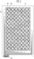
- FIG. 1 illustrates a plan view schematically showing a touch screen panel according to an embodiment.
- the touch screen panel may be a capacitive touch screen panel.
- the touch screen panel may include a transparent substrate 10; a plurality of first and second sensing patterns 12a and 12b on the transparent substrate 10; and position detecting lines 15 for connecting the first and second sensing patterns 12a and 12b to an external drive circuit (not illustrated) through a pad portion 20.
- the first sensing patterns 12a may be connected along a long-side direction of a screen and may be formed using a transparent electrode material, e.g., indium tin oxide (ITO).
- ITO indium tin oxide
- the first sensing patterns 12a may be connected along a column direction of the screen, so that the columns of the first sensing patterns 12a may be connected to the position detecting lines 15, respectively.
- the long-side direction of the screen is a horizontal direction
- the first sensing patterns 12a may be connected along a row direction of the screen.
- the long-side direction of the screen is the column direction, for convenience of illustration and description.
- the first sensing patterns 12a may be patterned to be connected along the column direction of the screen by a patterning process. Alternatively, the first sensing patterns 12a may have separated patterns from one another and the first sensing patterns 12a arranged in the same column may be connected by separate bridge patterns.
- the second sensing patterns 12b may be formed using a transparent electrode material.
- the second sensing patterns 12b may be connected along the short-side direction of the screen.
- the second sensing patterns 12b may be connected along a row direction of the screen, so that the rows of the second sensing patterns 12b may be connected to the position detecting lines 15, respectively.
- the second sensing patterns 12b may also be patterned to be connected along the row direction of the screen by a patterning process. Alternatively, the second sensing patterns 12b may have separated patterns from one another; and the second sensing patterns 12b arranged in the same row may be connected by separate bridge patterns.
- the second sensing patterns 12b when the first sensing patterns 12a are connected along the column direction of the screen by the patterning process, the second sensing patterns 12b may have separated patterns and may be connected along the row direction by the bridge patterns. In an alternative implementation, when the first sensing patterns 12a have separated patterns along the column direction of the screen and are connected by bridge patterns, the second sensing patterns 12b may be connected along the row direction of the screen by the patterning process.
- first and second sensing patterns 12a and 12b When the first and second sensing patterns 12a and 12b are positioned in different layers, they may all be patterned to be connected along the column and row directions by respective patterning processes.
- the position detecting lines 15 may connect the first and second sensing patterns 12a and 12b to the external drive circuit, e.g., a position detecting circuit, through the pad portion 20.
- the position detecting lines 15 may be disposed outside of an outline of the screen on which images are displayed, i.e., outside of a display area of the device.
- the position detecting lines 15 may have a wide range of selecting materials, and therefore, may be formed of a low-resistance material, e.g., molybdenum (Mo), silver (Ag), titanium (Ti), copper (Cu), aluminum (Al), and/or molybdenum/aluminum/molybdenum (Mo/Al/Mo), in addition to the transparent electrode material described above for forming the first and second sensing patterns 12a and 12b.
- Mo molybdenum
- Mo silver
- Ti titanium
- Cu copper
- Al aluminum
- Mo/Al/Mo molybdenum/aluminum/molybdenum
- a contact object e.g., a user's hand or a touch stick
- a change in capacitance based on a contact position may be transferred from the sensing patterns 12a and 12b to the external drive circuit via the position detecting lines 15 and the pad portion 20.
- the change in capacitance may be converted into an electrical signal by X and Y input processing circuits (not illustrated) and the like, so that the contact position may be detected.
- the aforementioned touch screen panel may be disposed on an independent substrate to be attached to a front face of an image display device and the like, or may be integrally implemented with a display panel of the image display device.
- the touch screen panel may be formed on an upper substrate of an organic light emitting display panel or liquid crystal display panel so as to be integrally implemented with the display panel.
- the touch screen panel may be integrally implemented with a display panel, thereby providing a thin image display device.
- base capacitance in the long-side direction of the screen may be about the same as that in the short-direction of the screen, and therefore, touch sensitivity may be enhanced.
- the base capacitance does not refer to touch capacitance used to implement the touch screen panel, but rather parasitic capacitance essentially generated in the structure of the touch screen panel.
- the parasitic capacitance generated between the respective first and second sensing patterns 12a and 12b and another component at a side of the display panel positioned beneath the touch screen panel e.g., a cathode electrode on a front face of the organic light emitting display panel or a common electrode on a front face of the liquid crystal display panel, may be a main factor.
- the parasitic capacitance generated between the first and second sensing patterns 12a and 12b and signal lines grounded at the side of the display panel may also be an auxiliary factor.
- the touch capacitance is the capacitance that implements the touch screen panel.
- the touch capacitance is the capacitance that is changed by a touch event in the occurrence of the touch event and which is used in position detection.
- the touch sensitivity of the touch screen panel may be enhanced when the base capacitance is small and the touch capacitance is large.
- the first sensing patterns 12a When the first sensing patterns 12a are connected along the long-side direction of the screen in a long line, the first sensing patterns 12a may be present in a number larger than that of the second sensing patterns 12b. Therefore, the base capacitance of the first sensing patterns 12a may be larger than that of the second sensing patterns 12b, while the touch capacitance of the first sensing patterns 12a may remain about equal to the touch capacitance of the second sensing patterns 12b. As a result, the touch sensitivity in the long-side direction of the screen may generally be low. Therefore, the entire touch sensitivity of the touch screen panel may also be lowered.
- the base capacitance which, as described above, may be greater in the long-side directions of the screen, may be reduced by decreasing an area of each of the first sensing patterns 12a.
- an area of each of the second sensing patterns 12b may be increased.
- the pattern shapes of the first and second sensing patterns 12a and 12b may be changed such that the area of each of the first sensing patterns 12a may be smaller than the area of each of the second sensing patterns 12b.
- the touch sensitivity of the touch screen panel may be enhanced.
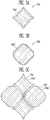
- FIGS. 2A to 2C illustrate plan views showing first and second sensing patterns according to an embodiment.
- each of the first and second sensing patterns 12a and 12b may be patterned using a polygon having the same shape and size as a basic form. As illustrated in FIG. 2A , the first sensing pattern 12a may be patterned to have a concave portion 12a1 recessed inward from each side of the polygon (i.e., concavely inward).
- each of the first and second sensing patterns 12a and 12b may be patterned using the same rhombus as a basic form (the dashed line illustrated in FIGS. 2A and 2B ).
- the first sensing pattern 12a may be patterned to have a concave portion 12a1 recessed inward by a predetermined distance from each of the sides of the rhombus.
- the base capacitance in each channel according to the long-side direction of the screen i.e., a channel of each of the column lines, may be decreased, thereby enhancing the touch sensitivity.
- the distance at which the first sensing pattern 12a is recessed inward from each of the sides thereof may be experimentally determined such that the base capacitance may be decreased in a range that satisfies a predetermined touch capacitance desired in the touch screen panel.
- the base capacitance in the long-side direction of the screen may be decreased by decreasing the area of the first sensing pattern 12a and the base capacitance in the short-side direction of the screen may be increased by increasing the area of the second sensing pattern 12b.
- the base capacitance in the long-side direction of the screen may be precisely matched to the base capacitance in the short-side directions of the screen.
- the areas of the first and second sensing patterns 12a and 12b may be adjusted such that the base capacitance in the long-side direction of the screen is substantially identical to, i.e., about equal to, that in the short-side direction of the screen.
- each of the second sensing patterns 12b may be patterned to have a projection portion 12b1 protruded outward from each side of a polygon, e.g., a rhombus.
- the first and second sensing patterns 12a and 12b may be positioned close to each other.
- a region for increasing the area of the second sensing patterns 12b i.e., the projection portion 12b1
- the projection portion 12b1 may be as wide as the decreased area of the first sensing patterns 12a, i.e., the concave portion 12a1.
- the projection portion 12b1 of each of the second sensing patterns 12b may protrude outwardly and may correspond to the area of the concave portion 12a1 of each of the first sensing patterns 12a. That is, the area of the concave portion 12a1 recessed inwardly on each of the first sensing patterns 12a may be similar or substantially identical to, i.e., about equal to, the area of the projection portion 12b1 protruding outwardly on each of the second sensing patterns 12b.
- the embodiments are not limited thereto.
- the area of the projection portion 12b1 of each of the second sensing patterns 12b may be smaller than the area of the concave portion 12a1 of each of the first sensing patterns 12a so that the first and second sensing patterns 12a and 12b may be positioned closer to each other.
- the area of the projection portion 12b1 of each of the second sensing patterns 12b may be larger than that of the concave portion 12a1 of each of the first sensing patterns 12a.
- the pattern shapes of the first and second sensing patterns 12a and 12b may be changed such that the base capacitance in the long-side directions of the screen may be matched to that in the short-side directions of the screen.
- the touch sensitivity in the long-direction of the screen may be similar or identical to, i.e., about equal to, that in the short-direction of the screen, thereby beneficially reducing errors in position detection and advantageously enhancing precision. Accordingly, the touch screen panel having enhanced touch sensitivity may be provided.
- the base capacitance in the long-side directions of a screen may be matched to that in the short-side directions of the screen. Accordingly, errors in position detection may be reduced and the touch sensitivity of the touch screen panel may be enhanced.
- FIGS. 3A to 3C illustrate plan views showing first and second sensing patterns according to another embodiment.
- FIGS. 3A to 3C repeated descriptions of portions identical to those of FIGS. 2A to 2C will be omitted.
- a first sensing pattern 12a' may be patterned to have a stepped concave portion 12a1' recessed inwardly on each side of a polygon basic shape.
- a second sensing pattern 12b' may be patterned to have a stepped projection portion 12b1' protruded outwardly on each side of the polygon basic shape.
- the vicinity of a vertex of the polygon connected to an adjacent first or second sensing pattern 12a' or 12b' may be designed to maintain its shape.
- the shapes and sizes of the first and second sensing patterns 12a, 12a', 12b, and 12b' according to the embodiments may be variously modified and implemented.
- first and second sensing patterns 12a, 12a', 12b, and 12b' may be patterned using the polygon as a basic form, the present invention is not limited thereto.
- the first and second sensing patterns may be patterned using a circle as a basic form.
- a diameter of each of the first sensing patterns connected along the long-side direction of the screen may be smaller than a diameter of each of the second sensing patterns connected along the short-side direction of the screen.
- the horizontal and vertical lengths of a screen may be different from each other. Accordingly, the touch sensitivity in a first direction may be different from that in a second direction.
- a larger number of sensing patterns may be connected in a long line, as compared with a short-side direction. Therefore, base capacitance may be increased by parasitic capacitance between electrodes and signal lines at a lower side of a display panel. Accordingly, the touch sensitivity may be lowered.
- the difference between the base capacitances in the long-side and short-side directions of the screen may be decreased by changing the pattern shapes of the sensing patterns, so that the touch screen panel having enhanced touch sensitivity may be provided.
Landscapes
- Engineering & Computer Science (AREA)
- General Engineering & Computer Science (AREA)
- Theoretical Computer Science (AREA)
- Human Computer Interaction (AREA)
- Physics & Mathematics (AREA)
- General Physics & Mathematics (AREA)
- Quality & Reliability (AREA)
- Position Input By Displaying (AREA)
Claims (7)
- Panneau d'écran tactile capacitif, comprenant :une pluralité de premiers motifs de détection (12a, 12a') reliés le long d'une direction du côté long d'un écran ; etune pluralité de deuxièmes motifs de détection (12b, 12b') reliés le long d'une direction du côté court de l'écran,dans lequel une zone de chacun des premiers motifs de détection (12a, 12a') est plus petite qu'une zone de chacun des deuxièmes motifs de détection (12b, 12b'), caractérisé en ce que :les premier et deuxième motifs de détection (12a, 12a', 12b, 12b') sont modelés sous forme d'un polygone avec la même forme et la même taille en tant que forme de base, etchacun des premiers motifs de détection (12a, 12a') a une partie concave (12a1, 12a1') en retrait vers l'intérieur sur chaque côté du polygone, où chacun des deuxièmes motifs de détection (12b, 12b') a une partie saillante (12b1, 12b1') faisant saillie vers l'extérieur sur chacun des côtés du polygone ; etdans lequel une zone de chacun des premiers motifs de détection (12a, 12a') et une zone de chacun des deuxièmes motifs de détection (12b, 12b') sont adaptées de manière à ce qu'une capacité de base générée entre une électrode de cathode ou une électrode commune du panneau d'affichage et la pluralité de premiers motifs de détection (12a, 12a') reliés le long de la direction du côté long de l'écran soit égale à une capacité de base générée entre l'électrode de cathode ou une électrode commune du panneau d'affichage et la pluralité des deuxièmes motifs de détection (12b, 12b') reliés le long de la direction du côté court de l'écran.
- Panneau d'écran tactile tel que revendiqué dans la revendication 1, dans lequel une zone de la partie saillante (12b1, 12b1') des deuxièmes motifs de détection (12b, 12b') correspond à une zone de la partie concave (12a1, 12a1') des premiers motifs de détection (12a, 12a').
- Panneau d'écran tactile tel que revendiqué dans la revendication 1, dans lequel :les premier et deuxième motifs de détection (12a, 12a', 12b, 12b') constituent un losange en tant que forme de base ;chacun des premiers motifs de détection (12a, 12a') a une partie concave (12a1, 12a1') en retrait vers l'intérieur sur chaque côté du losange ; etchacun des deuxièmes motifs de détection (12b, 12b') a une partie saillante (12b1, 12b1') faisant saillie vers l'extérieur sur chacun des côtés du losange.
- Panneau à écran tactile tel que revendiqué dans la revendication 3, dans lequel une zone de la partie concave (12a1, 12a1') en retrait vers l'intérieur sur chacun des premiers motifs de détection (12a, 12a') est égale à une zone de la partie saillante (12b1, 12b1') faisant saillie vers l'extérieur sur chacun des deuxièmes motifs de détection (12b, 12b').
- Panneau à écran tactile tel que revendiqué dans la revendication 3, dans lequel :la partie concave (12a1') est une partie concave étagée ayant au moins deux largeurs différentes ; etla partie saillante (12b1') est une partie saillante étagée ayant au moins deux largeurs différentes.
- Panneau à écran tactile tel que revendiqué dans l'une des revendications précédentes, comprenant en outre :un substrat transparent (10) sur lequel sont disposés les premier et deuxième motifs de détection (12a, 12a', 12b, 12b') ; etdes lignes de détection de position (15) adaptées pour relier des premier et deuxième motifs de détection (12a, 12a', 12b, 12b') à un circuit de commande externe.
- Panneau d'affichage pour afficher des images, comprenant :un panneau d'écran tactile tel que revendiqué dans l'une des revendications 1 à 6 ;un substrat supérieur sur lequel le panneau d'écran tactile est disposé de manière à être créé d'un seul tenant avec le panneau d'affichage.
Applications Claiming Priority (1)
| Application Number | Priority Date | Filing Date | Title |
|---|---|---|---|
| KR1020100022282A KR101113450B1 (ko) | 2010-03-12 | 2010-03-12 | 터치 스크린 패널 |
Publications (3)
| Publication Number | Publication Date |
|---|---|
| EP2390770A2 EP2390770A2 (fr) | 2011-11-30 |
| EP2390770A3 EP2390770A3 (fr) | 2013-07-17 |
| EP2390770B1 true EP2390770B1 (fr) | 2018-06-06 |
Family
ID=44559492
Family Applications (1)
| Application Number | Title | Priority Date | Filing Date |
|---|---|---|---|
| EP11157261.6A Active EP2390770B1 (fr) | 2010-03-12 | 2011-03-08 | Panneau d'écran tactile |
Country Status (4)
| Country | Link |
|---|---|
| US (1) | US20110221698A1 (fr) |
| EP (1) | EP2390770B1 (fr) |
| JP (1) | JP5224610B2 (fr) |
| KR (1) | KR101113450B1 (fr) |
Families Citing this family (11)
| Publication number | Priority date | Publication date | Assignee | Title |
|---|---|---|---|---|
| US8698767B2 (en) * | 2010-08-19 | 2014-04-15 | Samsung Display Co., Ltd. | Touch screen panel |
| KR101705557B1 (ko) * | 2010-11-24 | 2017-02-22 | 엘지디스플레이 주식회사 | 터치 스크린이 내장된 액정 표시장치 |
| JP5968507B2 (ja) * | 2011-10-05 | 2016-08-10 | 富士フイルム株式会社 | 導電シート、タッチパネル、表示装置 |
| JP5809117B2 (ja) * | 2011-10-05 | 2015-11-10 | 富士フイルム株式会社 | 導電シート、タッチパネル、表示装置 |
| KR101542043B1 (ko) | 2012-06-27 | 2015-08-06 | 엘지디스플레이 주식회사 | 터치 스크린 패널 |
| CN102855039B (zh) * | 2012-08-21 | 2015-09-09 | 信利半导体有限公司 | 一种电容式触摸屏架桥结构制作方法 |
| KR102239861B1 (ko) | 2014-11-26 | 2021-04-13 | 삼성디스플레이 주식회사 | 터치 센서를 포함하는 표시 장치 및 그 구동 방법 |
| KR102302139B1 (ko) * | 2015-01-27 | 2021-09-14 | 삼성디스플레이 주식회사 | 터치 표시 장치 및 그 구동 방법 |
| CN104730757B (zh) * | 2015-03-27 | 2017-10-27 | 京东方科技集团股份有限公司 | 彩膜基板、彩膜基板的制造方法、触摸屏及显示装置 |
| CN105786290A (zh) * | 2016-04-28 | 2016-07-20 | 京东方科技集团股份有限公司 | 触摸感测器件、触控面板、显示面板和显示装置 |
| US12287930B2 (en) * | 2019-04-24 | 2025-04-29 | Samsung Display Co., Ltd. | Non-rigid device and display device |
Family Cites Families (14)
| Publication number | Priority date | Publication date | Assignee | Title |
|---|---|---|---|---|
| TW200715176A (en) * | 2005-10-07 | 2007-04-16 | Elan Microelectronics Corp | Method for compensating sensitivity of sensor of touch panel |
| GB2439614B (en) * | 2006-05-31 | 2008-12-24 | Harald Philipp | Two-dimensional position sensor |
| TW200901014A (en) * | 2007-06-28 | 2009-01-01 | Sense Pad Tech Co Ltd | Touch panel device |
| KR20090015414A (ko) * | 2007-08-08 | 2009-02-12 | 에이디반도체(주) | 정전용량 터치감지패널 |
| JP5094376B2 (ja) * | 2007-12-28 | 2012-12-12 | 株式会社ワコム | 位置検出装置 |
| KR20090075369A (ko) * | 2008-01-04 | 2009-07-08 | 삼성전자주식회사 | 표시 패널 |
| KR101519844B1 (ko) * | 2008-01-07 | 2015-05-13 | 삼성디스플레이 주식회사 | 터치스크린패널용 상부기판, 그 제조방법 및 이를 갖는표시장치 |
| JP4945483B2 (ja) * | 2008-02-27 | 2012-06-06 | 株式会社 日立ディスプレイズ | 表示パネル |
| KR20090104192A (ko) * | 2008-03-31 | 2009-10-06 | 박철 | 정전용량 방식 터치스크린 전극 패턴 |
| JP5154316B2 (ja) * | 2008-06-30 | 2013-02-27 | 株式会社ジャパンディスプレイイースト | タッチパネル |
| JP5033078B2 (ja) * | 2008-08-06 | 2012-09-26 | 株式会社ジャパンディスプレイイースト | 表示装置 |
| KR101219242B1 (ko) * | 2009-01-16 | 2013-01-07 | 삼성디스플레이 주식회사 | 터치 스크린 패널 및 그 제조방법 |
| JP2010244357A (ja) * | 2009-04-07 | 2010-10-28 | Toshiba Mobile Display Co Ltd | 静電容量検知方式タッチパネル |
| US8593410B2 (en) * | 2009-04-10 | 2013-11-26 | Apple Inc. | Touch sensor panel design |
-
2010
- 2010-03-12 KR KR1020100022282A patent/KR101113450B1/ko not_active Expired - Fee Related
- 2010-07-29 JP JP2010170485A patent/JP5224610B2/ja active Active
- 2010-11-19 US US12/926,465 patent/US20110221698A1/en not_active Abandoned
-
2011
- 2011-03-08 EP EP11157261.6A patent/EP2390770B1/fr active Active
Non-Patent Citations (1)
| Title |
|---|
| None * |
Also Published As
| Publication number | Publication date |
|---|---|
| EP2390770A2 (fr) | 2011-11-30 |
| JP5224610B2 (ja) | 2013-07-03 |
| KR101113450B1 (ko) | 2012-02-29 |
| EP2390770A3 (fr) | 2013-07-17 |
| US20110221698A1 (en) | 2011-09-15 |
| JP2011192255A (ja) | 2011-09-29 |
| KR20110103117A (ko) | 2011-09-20 |
Similar Documents
| Publication | Publication Date | Title |
|---|---|---|
| EP2390770B1 (fr) | Panneau d'écran tactile | |
| CN105302399B (zh) | 触摸屏面板 | |
| US8279201B2 (en) | Touch screen panel and method of fabricating the same | |
| KR101448251B1 (ko) | 터치 스크린 패널 및 이를 구비한 표시 장치 | |
| EP2209064A1 (fr) | Panneau d'écran tactile et procédé de fabrication associé | |
| US8730191B2 (en) | Touch screen panel protected against failure due to static electricity | |
| CN102375596A (zh) | 触摸屏面板 | |
| US8963848B2 (en) | Touch screen panel | |
| KR101142664B1 (ko) | 터치패널 일체형 액정표시장치 및 그 제조방법 | |
| KR101976089B1 (ko) | 터치 스크린 패널 | |
| US9104276B2 (en) | Touch screen panel and manufacturing method thereof | |
| US8279195B2 (en) | Touch screen panel | |
| US20110227840A1 (en) | Touch screen panel and fabrication method thereof | |
| US20120062487A1 (en) | Touch Screen Panel and Display Device Having the Same | |
| US8749514B2 (en) | Touch screen panel | |
| KR20160085400A (ko) | 터치 센서 장치 및 이를 포함하는 표시 장치 | |
| US9904422B2 (en) | Mother substrate for a touch screen panel and array test method thereof | |
| KR101056264B1 (ko) | 터치 스크린 패널 | |
| US10521057B2 (en) | Touch screen panel having overlapping sensing electrodes and method of manufacturing the same | |
| KR101197701B1 (ko) | 터치 스크린 패널 | |
| KR101056312B1 (ko) | 터치 스크린 패널 | |
| KR20150025832A (ko) | 터치 검출 개선을 위한 터치 검출 장치 |
Legal Events
| Date | Code | Title | Description |
|---|---|---|---|
| AK | Designated contracting states |
Kind code of ref document: A2 Designated state(s): AL AT BE BG CH CY CZ DE DK EE ES FI FR GB GR HR HU IE IS IT LI LT LU LV MC MK MT NL NO PL PT RO RS SE SI SK SM TR |
|
| AX | Request for extension of the european patent |
Extension state: BA ME |
|
| PUAI | Public reference made under article 153(3) epc to a published international application that has entered the european phase |
Free format text: ORIGINAL CODE: 0009012 |
|
| RAP1 | Party data changed (applicant data changed or rights of an application transferred) |
Owner name: SAMSUNG DISPLAY CO., LTD. |
|
| PUAL | Search report despatched |
Free format text: ORIGINAL CODE: 0009013 |
|
| AK | Designated contracting states |
Kind code of ref document: A3 Designated state(s): AL AT BE BG CH CY CZ DE DK EE ES FI FR GB GR HR HU IE IS IT LI LT LU LV MC MK MT NL NO PL PT RO RS SE SI SK SM TR |
|
| AX | Request for extension of the european patent |
Extension state: BA ME |
|
| RIC1 | Information provided on ipc code assigned before grant |
Ipc: G06F 3/044 20060101AFI20130610BHEP |
|
| 17P | Request for examination filed |
Effective date: 20130910 |
|
| RAP1 | Party data changed (applicant data changed or rights of an application transferred) |
Owner name: SAMSUNG DISPLAY CO., LTD. |
|
| STAA | Information on the status of an ep patent application or granted ep patent |
Free format text: STATUS: EXAMINATION IS IN PROGRESS |
|
| 17Q | First examination report despatched |
Effective date: 20170503 |
|
| GRAP | Despatch of communication of intention to grant a patent |
Free format text: ORIGINAL CODE: EPIDOSNIGR1 |
|
| STAA | Information on the status of an ep patent application or granted ep patent |
Free format text: STATUS: GRANT OF PATENT IS INTENDED |
|
| INTG | Intention to grant announced |
Effective date: 20180102 |
|
| GRAS | Grant fee paid |
Free format text: ORIGINAL CODE: EPIDOSNIGR3 |
|
| GRAA | (expected) grant |
Free format text: ORIGINAL CODE: 0009210 |
|
| STAA | Information on the status of an ep patent application or granted ep patent |
Free format text: STATUS: THE PATENT HAS BEEN GRANTED |
|
| AK | Designated contracting states |
Kind code of ref document: B1 Designated state(s): AL AT BE BG CH CY CZ DE DK EE ES FI FR GB GR HR HU IE IS IT LI LT LU LV MC MK MT NL NO PL PT RO RS SE SI SK SM TR |
|
| REG | Reference to a national code |
Ref country code: GB Ref legal event code: FG4D |
|
| REG | Reference to a national code |
Ref country code: CH Ref legal event code: EP Ref country code: AT Ref legal event code: REF Ref document number: 1006813 Country of ref document: AT Kind code of ref document: T Effective date: 20180615 |
|
| REG | Reference to a national code |
Ref country code: IE Ref legal event code: FG4D |
|
| REG | Reference to a national code |
Ref country code: DE Ref legal event code: R096 Ref document number: 602011048973 Country of ref document: DE |
|
| REG | Reference to a national code |
Ref country code: NL Ref legal event code: FP |
|
| REG | Reference to a national code |
Ref country code: LT Ref legal event code: MG4D |
|
| PG25 | Lapsed in a contracting state [announced via postgrant information from national office to epo] |
Ref country code: NO Free format text: LAPSE BECAUSE OF FAILURE TO SUBMIT A TRANSLATION OF THE DESCRIPTION OR TO PAY THE FEE WITHIN THE PRESCRIBED TIME-LIMIT Effective date: 20180906 Ref country code: FI Free format text: LAPSE BECAUSE OF FAILURE TO SUBMIT A TRANSLATION OF THE DESCRIPTION OR TO PAY THE FEE WITHIN THE PRESCRIBED TIME-LIMIT Effective date: 20180606 Ref country code: BG Free format text: LAPSE BECAUSE OF FAILURE TO SUBMIT A TRANSLATION OF THE DESCRIPTION OR TO PAY THE FEE WITHIN THE PRESCRIBED TIME-LIMIT Effective date: 20180906 Ref country code: CY Free format text: LAPSE BECAUSE OF FAILURE TO SUBMIT A TRANSLATION OF THE DESCRIPTION OR TO PAY THE FEE WITHIN THE PRESCRIBED TIME-LIMIT Effective date: 20180606 Ref country code: SE Free format text: LAPSE BECAUSE OF FAILURE TO SUBMIT A TRANSLATION OF THE DESCRIPTION OR TO PAY THE FEE WITHIN THE PRESCRIBED TIME-LIMIT Effective date: 20180606 Ref country code: ES Free format text: LAPSE BECAUSE OF FAILURE TO SUBMIT A TRANSLATION OF THE DESCRIPTION OR TO PAY THE FEE WITHIN THE PRESCRIBED TIME-LIMIT Effective date: 20180606 Ref country code: LT Free format text: LAPSE BECAUSE OF FAILURE TO SUBMIT A TRANSLATION OF THE DESCRIPTION OR TO PAY THE FEE WITHIN THE PRESCRIBED TIME-LIMIT Effective date: 20180606 |
|
| PG25 | Lapsed in a contracting state [announced via postgrant information from national office to epo] |
Ref country code: RS Free format text: LAPSE BECAUSE OF FAILURE TO SUBMIT A TRANSLATION OF THE DESCRIPTION OR TO PAY THE FEE WITHIN THE PRESCRIBED TIME-LIMIT Effective date: 20180606 Ref country code: HR Free format text: LAPSE BECAUSE OF FAILURE TO SUBMIT A TRANSLATION OF THE DESCRIPTION OR TO PAY THE FEE WITHIN THE PRESCRIBED TIME-LIMIT Effective date: 20180606 Ref country code: LV Free format text: LAPSE BECAUSE OF FAILURE TO SUBMIT A TRANSLATION OF THE DESCRIPTION OR TO PAY THE FEE WITHIN THE PRESCRIBED TIME-LIMIT Effective date: 20180606 Ref country code: GR Free format text: LAPSE BECAUSE OF FAILURE TO SUBMIT A TRANSLATION OF THE DESCRIPTION OR TO PAY THE FEE WITHIN THE PRESCRIBED TIME-LIMIT Effective date: 20180907 |
|
| REG | Reference to a national code |
Ref country code: AT Ref legal event code: MK05 Ref document number: 1006813 Country of ref document: AT Kind code of ref document: T Effective date: 20180606 |
|
| PG25 | Lapsed in a contracting state [announced via postgrant information from national office to epo] |
Ref country code: PL Free format text: LAPSE BECAUSE OF FAILURE TO SUBMIT A TRANSLATION OF THE DESCRIPTION OR TO PAY THE FEE WITHIN THE PRESCRIBED TIME-LIMIT Effective date: 20180606 Ref country code: EE Free format text: LAPSE BECAUSE OF FAILURE TO SUBMIT A TRANSLATION OF THE DESCRIPTION OR TO PAY THE FEE WITHIN THE PRESCRIBED TIME-LIMIT Effective date: 20180606 Ref country code: IS Free format text: LAPSE BECAUSE OF FAILURE TO SUBMIT A TRANSLATION OF THE DESCRIPTION OR TO PAY THE FEE WITHIN THE PRESCRIBED TIME-LIMIT Effective date: 20181006 Ref country code: AT Free format text: LAPSE BECAUSE OF FAILURE TO SUBMIT A TRANSLATION OF THE DESCRIPTION OR TO PAY THE FEE WITHIN THE PRESCRIBED TIME-LIMIT Effective date: 20180606 Ref country code: RO Free format text: LAPSE BECAUSE OF FAILURE TO SUBMIT A TRANSLATION OF THE DESCRIPTION OR TO PAY THE FEE WITHIN THE PRESCRIBED TIME-LIMIT Effective date: 20180606 Ref country code: CZ Free format text: LAPSE BECAUSE OF FAILURE TO SUBMIT A TRANSLATION OF THE DESCRIPTION OR TO PAY THE FEE WITHIN THE PRESCRIBED TIME-LIMIT Effective date: 20180606 Ref country code: SK Free format text: LAPSE BECAUSE OF FAILURE TO SUBMIT A TRANSLATION OF THE DESCRIPTION OR TO PAY THE FEE WITHIN THE PRESCRIBED TIME-LIMIT Effective date: 20180606 |
|
| PG25 | Lapsed in a contracting state [announced via postgrant information from national office to epo] |
Ref country code: SM Free format text: LAPSE BECAUSE OF FAILURE TO SUBMIT A TRANSLATION OF THE DESCRIPTION OR TO PAY THE FEE WITHIN THE PRESCRIBED TIME-LIMIT Effective date: 20180606 Ref country code: IT Free format text: LAPSE BECAUSE OF FAILURE TO SUBMIT A TRANSLATION OF THE DESCRIPTION OR TO PAY THE FEE WITHIN THE PRESCRIBED TIME-LIMIT Effective date: 20180606 |
|
| REG | Reference to a national code |
Ref country code: DE Ref legal event code: R097 Ref document number: 602011048973 Country of ref document: DE |
|
| PLBE | No opposition filed within time limit |
Free format text: ORIGINAL CODE: 0009261 |
|
| STAA | Information on the status of an ep patent application or granted ep patent |
Free format text: STATUS: NO OPPOSITION FILED WITHIN TIME LIMIT |
|
| 26N | No opposition filed |
Effective date: 20190307 |
|
| PG25 | Lapsed in a contracting state [announced via postgrant information from national office to epo] |
Ref country code: SI Free format text: LAPSE BECAUSE OF FAILURE TO SUBMIT A TRANSLATION OF THE DESCRIPTION OR TO PAY THE FEE WITHIN THE PRESCRIBED TIME-LIMIT Effective date: 20180606 Ref country code: DK Free format text: LAPSE BECAUSE OF FAILURE TO SUBMIT A TRANSLATION OF THE DESCRIPTION OR TO PAY THE FEE WITHIN THE PRESCRIBED TIME-LIMIT Effective date: 20180606 |
|
| PG25 | Lapsed in a contracting state [announced via postgrant information from national office to epo] |
Ref country code: MC Free format text: LAPSE BECAUSE OF FAILURE TO SUBMIT A TRANSLATION OF THE DESCRIPTION OR TO PAY THE FEE WITHIN THE PRESCRIBED TIME-LIMIT Effective date: 20180606 |
|
| REG | Reference to a national code |
Ref country code: CH Ref legal event code: PL |
|
| PG25 | Lapsed in a contracting state [announced via postgrant information from national office to epo] |
Ref country code: AL Free format text: LAPSE BECAUSE OF FAILURE TO SUBMIT A TRANSLATION OF THE DESCRIPTION OR TO PAY THE FEE WITHIN THE PRESCRIBED TIME-LIMIT Effective date: 20180606 Ref country code: LU Free format text: LAPSE BECAUSE OF NON-PAYMENT OF DUE FEES Effective date: 20190308 |
|
| REG | Reference to a national code |
Ref country code: BE Ref legal event code: MM Effective date: 20190331 |
|
| PG25 | Lapsed in a contracting state [announced via postgrant information from national office to epo] |
Ref country code: CH Free format text: LAPSE BECAUSE OF NON-PAYMENT OF DUE FEES Effective date: 20190331 Ref country code: IE Free format text: LAPSE BECAUSE OF NON-PAYMENT OF DUE FEES Effective date: 20190308 Ref country code: LI Free format text: LAPSE BECAUSE OF NON-PAYMENT OF DUE FEES Effective date: 20190331 |
|
| PG25 | Lapsed in a contracting state [announced via postgrant information from national office to epo] |
Ref country code: BE Free format text: LAPSE BECAUSE OF NON-PAYMENT OF DUE FEES Effective date: 20190331 |
|
| PG25 | Lapsed in a contracting state [announced via postgrant information from national office to epo] |
Ref country code: TR Free format text: LAPSE BECAUSE OF FAILURE TO SUBMIT A TRANSLATION OF THE DESCRIPTION OR TO PAY THE FEE WITHIN THE PRESCRIBED TIME-LIMIT Effective date: 20180606 |
|
| PG25 | Lapsed in a contracting state [announced via postgrant information from national office to epo] |
Ref country code: MT Free format text: LAPSE BECAUSE OF NON-PAYMENT OF DUE FEES Effective date: 20190308 Ref country code: PT Free format text: LAPSE BECAUSE OF FAILURE TO SUBMIT A TRANSLATION OF THE DESCRIPTION OR TO PAY THE FEE WITHIN THE PRESCRIBED TIME-LIMIT Effective date: 20181008 |
|
| PG25 | Lapsed in a contracting state [announced via postgrant information from national office to epo] |
Ref country code: HU Free format text: LAPSE BECAUSE OF FAILURE TO SUBMIT A TRANSLATION OF THE DESCRIPTION OR TO PAY THE FEE WITHIN THE PRESCRIBED TIME-LIMIT; INVALID AB INITIO Effective date: 20110308 |
|
| PG25 | Lapsed in a contracting state [announced via postgrant information from national office to epo] |
Ref country code: MK Free format text: LAPSE BECAUSE OF FAILURE TO SUBMIT A TRANSLATION OF THE DESCRIPTION OR TO PAY THE FEE WITHIN THE PRESCRIBED TIME-LIMIT Effective date: 20180606 |
|
| P01 | Opt-out of the competence of the unified patent court (upc) registered |
Effective date: 20230515 |
|
| PGFP | Annual fee paid to national office [announced via postgrant information from national office to epo] |
Ref country code: NL Payment date: 20260220 Year of fee payment: 16 |
|
| PGFP | Annual fee paid to national office [announced via postgrant information from national office to epo] |
Ref country code: GB Payment date: 20260224 Year of fee payment: 16 |
|
| PGFP | Annual fee paid to national office [announced via postgrant information from national office to epo] |
Ref country code: DE Payment date: 20260220 Year of fee payment: 16 |
|
| PGFP | Annual fee paid to national office [announced via postgrant information from national office to epo] |
Ref country code: FR Payment date: 20260224 Year of fee payment: 16 |