EP2400622A2 - Induktiver Zellenausgleich - Google Patents
Induktiver Zellenausgleich Download PDFInfo
- Publication number
- EP2400622A2 EP2400622A2 EP20100189210 EP10189210A EP2400622A2 EP 2400622 A2 EP2400622 A2 EP 2400622A2 EP 20100189210 EP20100189210 EP 20100189210 EP 10189210 A EP10189210 A EP 10189210A EP 2400622 A2 EP2400622 A2 EP 2400622A2
- Authority
- EP
- European Patent Office
- Prior art keywords
- cell
- inductor
- terminal
- cells
- arrangement
- Prior art date
- Legal status (The legal status is an assumption and is not a legal conclusion. Google has not performed a legal analysis and makes no representation as to the accuracy of the status listed.)
- Withdrawn
Links
Images




Classifications
-
- H—ELECTRICITY
- H02—GENERATION; CONVERSION OR DISTRIBUTION OF ELECTRIC POWER
- H02J—ELECTRIC POWER NETWORKS; CIRCUIT ARRANGEMENTS OR SYSTEMS FOR SUPPLYING OR DISTRIBUTING ELECTRIC POWER; SYSTEMS FOR STORING ELECTRIC ENERGY
- H02J7/00—Circuit arrangements for charging or discharging batteries or for supplying loads from batteries
- H02J7/50—Circuit arrangements for charging or discharging batteries or for supplying loads from batteries acting upon multiple batteries simultaneously or sequentially
- H02J7/52—Circuit arrangements for charging or discharging batteries or for supplying loads from batteries acting upon multiple batteries simultaneously or sequentially for charge balancing, e.g. equalisation of charge between batteries
- H02J7/54—Passive balancing, e.g. using resistors or parallel MOSFETs
-
- H—ELECTRICITY
- H01—ELECTRIC ELEMENTS
- H01M—PROCESSES OR MEANS, e.g. BATTERIES, FOR THE DIRECT CONVERSION OF CHEMICAL ENERGY INTO ELECTRICAL ENERGY
- H01M10/00—Secondary cells; Manufacture thereof
- H01M10/42—Methods or arrangements for servicing or maintenance of secondary cells or secondary half-cells
-
- H—ELECTRICITY
- H01—ELECTRIC ELEMENTS
- H01M—PROCESSES OR MEANS, e.g. BATTERIES, FOR THE DIRECT CONVERSION OF CHEMICAL ENERGY INTO ELECTRICAL ENERGY
- H01M16/00—Structural combinations of different types of electrochemical generators
- H01M16/003—Structural combinations of different types of electrochemical generators of fuel cells with other electrochemical devices, e.g. capacitors, electrolysers
-
- Y—GENERAL TAGGING OF NEW TECHNOLOGICAL DEVELOPMENTS; GENERAL TAGGING OF CROSS-SECTIONAL TECHNOLOGIES SPANNING OVER SEVERAL SECTIONS OF THE IPC; TECHNICAL SUBJECTS COVERED BY FORMER USPC CROSS-REFERENCE ART COLLECTIONS [XRACs] AND DIGESTS
- Y02—TECHNOLOGIES OR APPLICATIONS FOR MITIGATION OR ADAPTATION AGAINST CLIMATE CHANGE
- Y02E—REDUCTION OF GREENHOUSE GAS [GHG] EMISSIONS, RELATED TO ENERGY GENERATION, TRANSMISSION OR DISTRIBUTION
- Y02E60/00—Enabling technologies; Technologies with a potential or indirect contribution to GHG emissions mitigation
- Y02E60/10—Energy storage using batteries
-
- Y—GENERAL TAGGING OF NEW TECHNOLOGICAL DEVELOPMENTS; GENERAL TAGGING OF CROSS-SECTIONAL TECHNOLOGIES SPANNING OVER SEVERAL SECTIONS OF THE IPC; TECHNICAL SUBJECTS COVERED BY FORMER USPC CROSS-REFERENCE ART COLLECTIONS [XRACs] AND DIGESTS
- Y02—TECHNOLOGIES OR APPLICATIONS FOR MITIGATION OR ADAPTATION AGAINST CLIMATE CHANGE
- Y02E—REDUCTION OF GREENHOUSE GAS [GHG] EMISSIONS, RELATED TO ENERGY GENERATION, TRANSMISSION OR DISTRIBUTION
- Y02E60/00—Enabling technologies; Technologies with a potential or indirect contribution to GHG emissions mitigation
- Y02E60/30—Hydrogen technology
- Y02E60/50—Fuel cells
-
- Y—GENERAL TAGGING OF NEW TECHNOLOGICAL DEVELOPMENTS; GENERAL TAGGING OF CROSS-SECTIONAL TECHNOLOGIES SPANNING OVER SEVERAL SECTIONS OF THE IPC; TECHNICAL SUBJECTS COVERED BY FORMER USPC CROSS-REFERENCE ART COLLECTIONS [XRACs] AND DIGESTS
- Y02—TECHNOLOGIES OR APPLICATIONS FOR MITIGATION OR ADAPTATION AGAINST CLIMATE CHANGE
- Y02T—CLIMATE CHANGE MITIGATION TECHNOLOGIES RELATED TO TRANSPORTATION
- Y02T10/00—Road transport of goods or passengers
- Y02T10/60—Other road transportation technologies with climate change mitigation effect
- Y02T10/70—Energy storage systems for electromobility, e.g. batteries
Definitions
- the cells can be battery cells or capacitor (super capacitor) cells.
- capacitor super capacitor
- One example of particular interest is the cells used in electric vehicle battery packs.
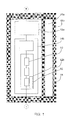
- Figure 1 shows a simplified block diagram of a battery pack with components as defined below:
- a "pack” or “battery pack” 18 is a group of parallel-connected slices 16 that make up the total battery as used in the application.
- the parallel connection increases the energy content and power capabilities of the battery pack, but not its voltage.
- the battery pack 18 consists of just one single slice 16. Depending on the application, the voltage is somewhere in the range of 100V to 600V (same as the slice voltage).
- Figures 2 to 4 show three different approaches to cell-balancing that are in use today.
- Figure 2 shows a passive cell-balancer.
- the cell 10 with the highest charge is simply (partly) discharged by switching a resistor 20 across it.
- this approach is mainly used in hybrid electric vehicles, as the engine can supply enough energy to the battery pack to keep the driving range at an acceptable level.
- Figure 3 shows a capacitive system. Charge is moved between two adjacent cells 10 by a capacitor 30. If all capacitors move between their cells often enough, the charge in all cells will become equal.
- Figure 4 is an example of a class of systems based on inductors and transformers.
- the highest charged cell 10 is connected to the inductor 40 by a switch 42.
- the current in the inductor will rise with time. After a predetermined amount of time the switch 42 is opened. As the current in the inductor cannot instantly change, it will find a way through the diode which is parallel to the other switch (of a lower voltage cell). The current will now charge the other battery cell, until the current has decayed to (nearly) zero and the diode stops conducting.
- Figure 5 shows how the inductive cell-balancing sections must be combined to form long chains.
- Two sections 12a,12b share one battery cell 50, the highest cell of one section 12b serves as the lowest cell of the next section 12a (by “next" section is meant the next section at a higher voltage).
- the other components are not shared between sections.
- the lowest cell of the section M is also the highest cell of section M-1. Applying this rule, arbitrarily long chains can be created.
- the system of Figure 5 needs N-1 inductors for a chain of N battery cells. So in a long chain (e.g. 100 cells) one needs roughly one inductor per battery cell.
- the system of Figure 2 has the big advantage that it is very low cost, as it does not need any capacitors, inductors, or transformers.
- the systems of Figure 3 and Figure 4 need more or less one reactive component per section of the series-connected chain of battery cells and are therefore more costly. They do, however, have the advantage of a higher efficiency.
- the resistive method has a 0% efficiency as it burns off all excess power of all cells, except the lowest charged cells.
- the capacitive system burns 50% of the energy difference of the cells that it balances.
- the efficiency of an inductive system can be nearly 100%.
- an energy storage cell arrangement comprising:
- This arrangement enables the inductor, used for energy transfer between cells, to be shared between cells.
- the cell terminals of the first set are different to those of the second set. This provides the smallest number of connections to enable any cell terminal to be coupled to one or other terminal of the inductor.
- the switching arrangement can comprise a respective switch between each cell terminal and one of the inductor terminals, and a respective diode in parallel with each switch. This provides an arrangement with a switch and diode for each cell terminal, thus providing a small amount of additional circuitry.
- the switching arrangement comprises a respective switch between each cell terminal and one of the inductor terminals, a respective diode between each inductor terminal and the top cell terminal and a respective diode between each inductor terminal and the bottom cell terminal. This arrangement needs only four diodes.
- the switching arrangement comprises a first three-way switch at the input to one of the inductor terminals, a second three-way switch at the input to the other of the inductor terminals, and a respective switch between each cell terminal and both of the three-way switches, wherein the three way switches are controlled such that each respective switch is connected to one or other of the inductor terminals.
- the switching arrangement can comprise a first diode between the one inductor terminal and the top cell terminal and a second diode between the other inductor terminal and the bottom cell terminal.
- This arrangement needs only two diodes, at the expense of having more switches in the circuit.
- the cell terminals of the first set can include all cell terminals and the cell terminals of the second set can include all cell terminals. This provides most flexibility, in that all cell terminals can be connected to either inductor terminal.
- the switching arrangement comprises a respective switch between each cell terminal and one of the inductor terminals, a respective switch between each cell terminal and the other of the inductor terminals, and a respective diode between the one inductor terminal and the top cell terminal and a respective diode between the other inductor terminal and the bottom cell terminal.
- This arrangement requires only two diodes, but has two switches associated with each cell terminal.
- the switching arrangement comprises a respective diode between each inductor terminal and the top cell terminal and a respective diode between each inductor terminal and the bottom cell terminal.
- the arrangement can further comprise a controller adapted to:
- This control of the switching enables a desired transfer of energy between cells.
- the invention also provides an electric vehicle battery cell pack comprising one or more battery cell arrangements of the invention.
- the invention also provides a method of performing cell balancing within an energy storage cell arrangement which comprises a series arrangement of cells, comprising at least two cells and an inductor shared between all cells, the method comprising identifying a cell or cells from which charge is to be removed; controlling a switching arrangement to transfer energy from the identified cell or cells to the shared inductor; and controlling the switching arrangement to transfer energy from the inductor to another cell or cells.
- the invention provides an energy storage cell arrangement in which a shared inductor is used.
- a switching arrangement is controllable such that it is able to couple one side of the inductor to any one of a first set of cell terminals, and to couple the other side of the inductor to any one of a second set of cell terminals, wherein the first and second sets of cell terminals together comprise all cell terminals of the series arrangement. In this way, energy can be transferred between cells in a configurable way, using a shared inductor.
- Figure 6 shows an arrangement in which (theoretically) one inductor 60 can balance an arbitrarily long chain of cells.
- relatively short sections e.g. three or four cells and one inductor 60 will be combined to a longer chain.
- the use of short sections keeps the specification of the switches and diodes realistic.
- each cell terminal (because of the series connection of cells 10, there are four electrical cell terminals for the three cells shown) is connected through a respective switch 62 to one terminal 64a of the inductor, and through another respective switch 62 to the other terminal 64b of the inductor.
- a respective diode 66a is connected between the one inductor terminal 64a and the top cell terminal 68.
- a respective diode 66b is connected between the other inductor terminal 64b and the top cell terminal 68.
- a respective diode 66c is connected between the one inductor terminal 64a and the bottom cell terminal 70.
- a respective diode 66d is connected between the other inductor terminal 64b and the bottom cell terminal 70.
- the diodes provide a current path to the series of cells so that inductor current is maintained flowing even if all the switches are open.
- the diode orientation is such that the cells cannot discharge through the diodes.
- the circuit made from the diodes and cells has the diodes and cells in a loop with the diodes reverse biased by the cell voltage.
- the inductor in Figure 6 can be thought of as a "flying" inductor. It can take energy from an arbitrary (subgroup of) cell(s) and dump that energy in another arbitrary (subgroup of) cell(s). It is important to note that energy, not charge, must be pumped from one cell to another. If charge is pumped, the efficiency of the circuit will be equal to that of a capacitive cell-balancer (i.e. 50% of the initial energy difference of the cell is lost). To make sure energy is pumped, the inductor must be connected to the cell that is charged until the current has dropped to zero.
- the circuit will start to act like a combination of an energy pump and a charge pump. If the switching frequency is so high that a DC current flows through the coil, then the circuit operates as a pure charge pump.
- Figure 7 shows the current paths in the circuit of Figure 6 when energy is pumped from the top cell to the bottom cell.
- Path 80 shows the discharge of the highest charged cell, which in this case is the top cell. This builds flux in the inductor. For this purpose, one switch couples the top cell terminal to the inductor terminal 64a and another switch couples the second cell terminal down to the inductor terminal 64b.
- Path 82 shows the spill-over during switching from discharging to charging, and it drives current through the diodes.
- Path 84 shows the path for inductor current to flow through the bottom cell.
- one switch couples the bottom cell terminal to the inductor terminal 64a and another switch couples the second cell terminal up to the inductor terminal 64b.
- Figure 8 shows a modification which enables a saving of two diodes from the circuit of Figure 6 .
- the current in the inductor has to return to zero before the next packet of energy can be moved from one cell to another. It is therefore possible to choose the direction of the current in the inductor each time a new energy transfer cycle is started. If the current in the inductor 60 always flows in the same direction, the same two diodes will always carry the spill-over current. In this way, the other two diodes can be eliminated from the circuit without any penalty.
- the desired current flow can be assured by connecting the inductor with the correct polarity.
- the circuit of Figure 8 needs 2*(N+1) switches, with N the number of cells.
- Figure 9 shows a circuit with a reduction in the number of switches.
- the switching arrangement comprises a first three-way switch 90 at the input to one of the inductor terminals 64a, a second three-way switch 92 at the input to the other of the inductor terminals 64b, and a respective switch 94 between each cell terminal and both of the three-way switches.
- the three way switches 90,92 are controlled such that each switch 94 is connected to or one other of the inductor terminals.
- a first diode is between the one inductor terminal 64a and the top cell terminal 68 and a second diode is between the other inductor terminal 64b and the bottom cell terminal 70.
- the toggle switches 90,92 and the switches 94 are in series, and Figure 9 thus shows that (particularly for sections of more than three cells) switches can be saved by using series-connected switches for cell selection and coil-current direction.
- Figures 8 and 9 are derived from the circuit of Figure 6 .
- the circuit of Figure 6 offers a lot of flexibility regarding the choice of cells to transfer energy between, and the direction of the currents. As Figures 8 and 9 show, giving up some flexibility results in a reduced number of components in the circuit.
- Figure 10 takes this approach a step further.
- the direction of the inductor current cannot be freely chosen in this circuit.
- the number of switches can be halved with respect to Figure 6 .
- the direction of the inductor current can no longer be fixed, it is not possible to remove diodes.
- a first set of cell terminals (the first and third) are connected through respective switches 100 to the one inductor terminal 64a and a second set of cell terminals (the second and fourth) are connected through respective switches 102 to the other inductor terminal 64b.
- a respective diode is between each inductor terminal and the top cell terminal and a respective diode is between each inductor terminal and the bottom cell terminal (i.e. the same diode arrangement as in Figure 6 ).
- the diodes are moved such that they are parallel to the switches 100,102.
- the switches will be NMOS and PMOS transistors.
- the diodes of Figure 11 can then simply be the (parasitic) drain-to-bulk diodes of the MOS transistors. This means that although they are important for the operation of the circuit, they don't show up as individual components in the layout. In this way, the circuit of Figure 11 will be smaller than the circuit of Figure 10 .
- circuits of Figure 10 and Figure 11 behave nearly identically, but there is one important difference: the sections of Figure 10 can be arbitrarily long, whereas the sections of Figure 11 should preferably be limited to a length of three cells per section. If the sections of Figure 11 are made longer, the diodes can cause short circuits.
- the inductor of Figure 6 can be regarded as a "flying" inductor as it can transfer energy form any cell to any other cell.
- the inductor of Figure 11 is more like a “rolling” inductor. It can only transfer energy from odd-numbered to even-numbered cells and vice versa.
- the table shows that the circuit of Figure 11 is particularly interesting. It needs exactly the same number of switches and diodes, but only half the number of inductors to serve the same number of cells as the circuit of Figure 4 . On top of that, if the circuit diagrams of complete battery packs made with sections of either Figure 4 or Figure 11 are compared, it shows that the circuit topology of both circuits is exactly identical for the cells, the switches, and the diodes. Only the inductors are connected differently.
- Figure 12 shows the circuit of Figure 5 , with the two inductors 120,122, and the same circuit but with inductor 124 instead of inductors 120 and 122 then corresponds to Figure 11 .
- a first disadvantage is that the worst case balancing time of Figure 11 is two times longer than that of Figure 4 (if the same component values are used). If only unbalance between two neighbouring cells has to be eliminated, the balancing time of the two circuits will be equal. But, if energy has to be moved between cells over a longer distance, the balancing time may take up to two times longer. The reason for this very simple: each inductor can move a certain amount of energy per clock cycle. So two inductors can move twice as much energy per clock cycle.
- N N N N N inductors N-1 N-1)/(M-1) (N-1)/(M-1) (N-1)/(M-1) switches 2*(N-1) 2*(M+1)*(N-1)/(M-1) (M+5)*(N-1)/(M-1) (M+1)*(N-1)/(M-1) diodes 2*(N-1) 2*(N-1)/(M-1) 2*(N-1)/(M-1) 4*(N-1)/(M-1)
- Figure 13 shows a circuit in which the ideal switches of Figure 11 have been replaced by NMOS and PMOS transistors T1 to T4. As stated above, the diodes D1 to D4 connected across the transistors can be replaced by the transistor body diodes.
- a better approach is to use the fact that energy is always pumped from a higher-charged to a lower-charged cell. This is equivalent to pumping from a higher-voltage to a lower-voltage cell (assuming the cells have the same temperature).
- Per unit time the current change in the inductor is higher when connected to the highest-charged cell. If the switch across the flyback diode is kept closed exactly as long as the switch that connects the inductor to the highest-charged cell, the current in the inductor will still be (slightly) higher than zero by the time the switch is opened across the flyback diode. The flyback diode now only has to conduct the "tail" of the flyback current.
- Figure 14 shows the functional gate voltages (i.e. high level means transistor acts as a closed switch, irrespective of whether the transistor is N or P-type) of the switches and the absolute value of the currents through the inductor, switches and diode D3.
- Figure 14 shows the signal waveforms of Figure 13 and the signals are shown for the case where energy is pumped from the top cell to the centre cell.
- the left set of plots shows the case where the second phase is carried out without using flyback switching as explained above.
- transistors T1 and T2 are turned on, and the inductor current rises, sourced from the top cell. T1 is then turned off. The inductor current then flows to the second cell through the diodes D2, D3. The second cell, the diodes D2 and D3 and the inductor from a closed circuit. Transistor T2 is shown turned on during this time but the current flow (in the reverse direction) is through the diode D2. All transistors are off before the next cycle begins.
- the right set of plots shows the case where the second phase is carried out using flyback switching as explained above.
- the transistor T3 In the second phase (energy transfer to the second cell), the transistor T3 is turned on for the initial part of the inductor current timing. This means that current flow is through the transistor T3 (in the forward direction) rather than through diode D3 while T3 is turned on. Only the small inductor current tail is driven through diode D3.
- Circuits for the measurement of cell voltage for use in cell balancing are already known and in use, and these do not need any modification for use in the invention. They form part of a control circuit for the section, and such a control circuit (as can be used to implement the invention) is shown schematically in Figure 1 as 19, as part of the section 12b.
- a cell can be replaced by a group of cells. This means it is fairly easy to make a hierarchical cell-balancing system. In the lowest level sections composed of battery cells are balanced, in the highest level sections of battery modules are balanced. The circuit topologies are the same, but the specification of the components of the different levels are, of course, very different as the voltage of a module is roughly ten times the voltage of a cell.
Landscapes
- Engineering & Computer Science (AREA)
- Power Engineering (AREA)
- Manufacturing & Machinery (AREA)
- Chemical & Material Sciences (AREA)
- Chemical Kinetics & Catalysis (AREA)
- Electrochemistry (AREA)
- General Chemical & Material Sciences (AREA)
- Charge And Discharge Circuits For Batteries Or The Like (AREA)
- Secondary Cells (AREA)
- Battery Mounting, Suspending (AREA)
Priority Applications (5)
| Application Number | Priority Date | Filing Date | Title |
|---|---|---|---|
| EP20100189210 EP2400622A3 (de) | 2010-06-28 | 2010-10-28 | Induktiver Zellenausgleich |
| US13/164,998 US20110316344A1 (en) | 2010-06-28 | 2011-06-21 | Inductive cell balancing |
| CN201510575210.8A CN105244937A (zh) | 2010-06-28 | 2011-06-24 | 能量存储单元装置、电池组和单元平衡方法 |
| CN2011101730012A CN102299565A (zh) | 2010-06-28 | 2011-06-24 | 电感性单元平衡 |
| JP2011142074A JP5367021B2 (ja) | 2010-06-28 | 2011-06-27 | エネルギー蓄積セル配列及び電気ビークルバッテリセルパック |
Applications Claiming Priority (2)
| Application Number | Priority Date | Filing Date | Title |
|---|---|---|---|
| EP10167520 | 2010-06-28 | ||
| EP20100189210 EP2400622A3 (de) | 2010-06-28 | 2010-10-28 | Induktiver Zellenausgleich |
Publications (2)
| Publication Number | Publication Date |
|---|---|
| EP2400622A2 true EP2400622A2 (de) | 2011-12-28 |
| EP2400622A3 EP2400622A3 (de) | 2012-03-14 |
Family
ID=44802550
Family Applications (1)
| Application Number | Title | Priority Date | Filing Date |
|---|---|---|---|
| EP20100189210 Withdrawn EP2400622A3 (de) | 2010-06-28 | 2010-10-28 | Induktiver Zellenausgleich |
Country Status (4)
| Country | Link |
|---|---|
| US (1) | US20110316344A1 (de) |
| EP (1) | EP2400622A3 (de) |
| JP (1) | JP5367021B2 (de) |
| CN (2) | CN105244937A (de) |
Cited By (7)
| Publication number | Priority date | Publication date | Assignee | Title |
|---|---|---|---|---|
| CN103545872A (zh) * | 2012-07-13 | 2014-01-29 | 蔡富生 | 平衡电池单元的平衡电路 |
| WO2015108111A1 (ja) * | 2014-01-15 | 2015-07-23 | Connexx Systems 株式会社 | ハイブリッド蓄電池、ならびにそれを利用するハイブリッド蓄電装置、発蓄電ユニット、電力網システムおよび走行体 |
| EP2916423A1 (de) * | 2014-03-04 | 2015-09-09 | Ricoh Company, Ltd. | Verfahren zur steuerung einer speicherstatuseinstellschaltung und speicherbatteriepack |
| DE102014215724A1 (de) | 2014-08-08 | 2016-02-11 | Robert Bosch Gmbh | Batteriezellmodul mit einer Ladezustandsausgleichseinheit zum Durchführen eines Ladezustandsausgleiches zwischen den Batteriezellen des Batteriezellmoduls und entsprechendes Verfahren |
| DE102014221867A1 (de) | 2014-10-27 | 2016-04-28 | Robert Bosch Gmbh | Verfahren und Schaltungsanordnung zum aktiven Cell-Balancing eines elektrischen Energiespeichers |
| DE102016012022A1 (de) | 2016-10-07 | 2017-04-27 | Daimler Ag | Elektrischer Akkumulator und Verfahren zum Betreiben eines solchen elektrischen Akkumulators |
| WO2017125193A1 (en) * | 2015-12-04 | 2017-07-27 | Technische Universiteit Eindhoven | Flexbattery |
Families Citing this family (30)
| Publication number | Priority date | Publication date | Assignee | Title |
|---|---|---|---|---|
| CN102111003B (zh) * | 2011-02-21 | 2013-07-17 | 成都芯源系统有限公司 | 新型电池均衡电路及其调节方法 |
| US9128165B2 (en) | 2011-05-04 | 2015-09-08 | Datang Nxp Semiconductors Co., Ltd. | Battery cell impedance measurement method and apparatus |
| US9225179B2 (en) * | 2011-10-12 | 2015-12-29 | Texas Instruments Incorporated | Capacitor-based active balancing for batteries and other power supplies |
| US9203121B2 (en) | 2011-10-12 | 2015-12-01 | Texas Instruments Incorporated | Inductor-based active balancing for batteries and other power supplies |
| CN103248077B (zh) * | 2012-02-08 | 2016-05-18 | 东莞赛微微电子有限公司 | 电池均衡电路 |
| JP2013192371A (ja) * | 2012-03-14 | 2013-09-26 | Sumitomo Electric Ind Ltd | 蓄電装置、充電方法及び放電方法 |
| CN102738860B (zh) * | 2012-06-04 | 2015-07-29 | 成都芯源系统有限公司 | 电池均衡装置和堆叠均衡装置 |
| CN103036277B (zh) * | 2012-11-28 | 2014-11-19 | 惠州市华阳集团股份有限公司 | 一种动力和储能电池组的均衡电路 |
| FR3001089B1 (fr) * | 2013-01-11 | 2016-09-09 | Enerstone | Equilibrage de charge dans une batterie electrique |
| US9472961B2 (en) | 2013-02-25 | 2016-10-18 | Semiconductor Components Industries, Llc | Method of forming a balancing circuit for a plurality of battery cells and structure therefor |
| DE102013021535A1 (de) * | 2013-12-18 | 2015-06-18 | Liebherr-Components Biberach Gmbh | Elektrische Energiespeichervorrichtung mit Symmetrierschaltung |
| KR102237034B1 (ko) * | 2014-02-18 | 2021-04-06 | 주식회사 실리콘웍스 | 다양한 밸런싱 동작 모드가 가능한 밸런싱 장치 및 그 방법 |
| US9977452B2 (en) * | 2014-03-07 | 2018-05-22 | Board Of Trustees Of The University Of Alabama | Multi-input or multi-output energy system architectures and control methods |
| KR20160099357A (ko) * | 2015-02-12 | 2016-08-22 | 삼성에스디아이 주식회사 | 배터리 팩 및 이를 포함하는 배터리 시스템 |
| KR101717077B1 (ko) * | 2016-07-15 | 2017-03-16 | 포항공과대학교 산학협력단 | 단일 인덕터를 이용한 배터리셀 밸런싱 회로 |
| JP6828296B2 (ja) * | 2016-08-09 | 2021-02-10 | 株式会社Gsユアサ | 蓄電装置および蓄電装置の充電制御方法 |
| CN106602648B (zh) * | 2016-12-14 | 2023-08-22 | 华南理工大学 | 一种基于电感储能的串联电池组双向无损均衡的改良电路 |
| CN106786865B (zh) * | 2016-12-14 | 2023-07-18 | 华南理工大学 | 一种基于电容储能的串联电池组双向无损均衡电路 |
| KR102123048B1 (ko) * | 2017-01-10 | 2020-06-15 | 주식회사 엘지화학 | 에너지 절약 및 빠른 셀 밸런싱이 가능한 충전 제어 장치 및 방법 |
| KR101856037B1 (ko) * | 2017-02-02 | 2018-05-09 | 포항공과대학교 산학협력단 | 단일 인덕터를 이용한 배터리 모듈 밸런싱 방법 |
| US11876394B2 (en) | 2017-12-21 | 2024-01-16 | Eric Paul Grasshoff | Active cell balancing in batteries using switch mode dividers |
| US10910847B2 (en) | 2017-12-21 | 2021-02-02 | Eric Paul Grasshoff | Active cell balancing in batteries using switch mode dividers |
| JP7006530B2 (ja) * | 2018-07-19 | 2022-01-24 | トヨタ自動車株式会社 | 蓄電デバイスの検査方法および製造方法 |
| KR102821612B1 (ko) | 2019-11-18 | 2025-06-16 | 주식회사 엘지에너지솔루션 | 셀 균등화 장치, 이를 포함하는 배터리 장치 및 셀 균등화 방법 |
| CN112217253A (zh) * | 2020-09-28 | 2021-01-12 | 长安大学 | 一种电池组双层拓扑结构均衡电路及方法 |
| CN112511046A (zh) * | 2020-12-09 | 2021-03-16 | 航天时代飞鸿技术有限公司 | 一种无人机弹射器快速刹车及能量回收电路 |
| GB2609999B (en) * | 2021-08-20 | 2024-01-31 | Cirrus Logic Int Semiconductor Ltd | Cell balancing |
| KR102923109B1 (ko) * | 2022-01-26 | 2026-02-06 | 한국전력공사 | 능동형 타입의 슈퍼 커패시터 셀 평형 유지 장치 및 이의 제어 방법 |
| GB2615610B (en) * | 2022-02-15 | 2026-03-11 | Cirrus Logic Int Semiconductor Ltd | Cell balancing |
| WO2025245583A1 (en) * | 2024-05-29 | 2025-12-04 | Relectrify Holdings Pty Ltd | Battery charge distribution based on reactive load |
Family Cites Families (11)
| Publication number | Priority date | Publication date | Assignee | Title |
|---|---|---|---|---|
| US5631534A (en) * | 1995-08-21 | 1997-05-20 | Delco Electronics Corp. | Bidirectional current pump for battery charge balancing |
| DE19645891A1 (de) * | 1996-11-07 | 1998-05-14 | Rainer Glaschick | Batterie-Stromversorgung |
| JP4378009B2 (ja) * | 1999-12-28 | 2009-12-02 | Fdk株式会社 | 直列接続された2次電池のバランス補正方法および装置 |
| US7378818B2 (en) * | 2002-11-25 | 2008-05-27 | Tiax Llc | Bidirectional power converter for balancing state of charge among series connected electrical energy storage units |
| US20070001651A1 (en) * | 2004-07-02 | 2007-01-04 | Harvey Troy A | Distributed networks of electric double layer capacitor supervisory controllers and networks thereof |
| JP4621635B2 (ja) * | 2006-07-05 | 2011-01-26 | Fdk株式会社 | 直列セルの電圧バランス補正回路 |
| JP4819902B2 (ja) * | 2006-09-15 | 2011-11-24 | 三菱電機株式会社 | Dc/dc電力変換装置 |
| CN101621218B (zh) * | 2008-06-30 | 2010-10-27 | 上海三玖电气设备有限公司 | 一种超级电容自动平衡控制系统 |
| DE102008043593A1 (de) * | 2008-11-10 | 2010-05-12 | Robert Bosch Gmbh | Angleichen elektrischer Spannungen von Gruppen elektrischer Speichereinheiten |
| JP5334566B2 (ja) * | 2008-12-25 | 2013-11-06 | Fdk株式会社 | 蓄電モジュールの電圧補正制御方法 |
| US8786255B2 (en) * | 2010-05-03 | 2014-07-22 | Infineon Technologies Ag | Active charge balancing circuit |
-
2010
- 2010-10-28 EP EP20100189210 patent/EP2400622A3/de not_active Withdrawn
-
2011
- 2011-06-21 US US13/164,998 patent/US20110316344A1/en not_active Abandoned
- 2011-06-24 CN CN201510575210.8A patent/CN105244937A/zh active Pending
- 2011-06-24 CN CN2011101730012A patent/CN102299565A/zh active Pending
- 2011-06-27 JP JP2011142074A patent/JP5367021B2/ja not_active Expired - Fee Related
Non-Patent Citations (1)
| Title |
|---|
| None |
Cited By (10)
| Publication number | Priority date | Publication date | Assignee | Title |
|---|---|---|---|---|
| CN103545872A (zh) * | 2012-07-13 | 2014-01-29 | 蔡富生 | 平衡电池单元的平衡电路 |
| WO2015108111A1 (ja) * | 2014-01-15 | 2015-07-23 | Connexx Systems 株式会社 | ハイブリッド蓄電池、ならびにそれを利用するハイブリッド蓄電装置、発蓄電ユニット、電力網システムおよび走行体 |
| EP2916423A1 (de) * | 2014-03-04 | 2015-09-09 | Ricoh Company, Ltd. | Verfahren zur steuerung einer speicherstatuseinstellschaltung und speicherbatteriepack |
| US9641003B2 (en) | 2014-03-04 | 2017-05-02 | Ricoh Company, Ltd. | Method of controlling switch circuit, storage status adjusting circuit, and storage battery pack |
| DE102014215724A1 (de) | 2014-08-08 | 2016-02-11 | Robert Bosch Gmbh | Batteriezellmodul mit einer Ladezustandsausgleichseinheit zum Durchführen eines Ladezustandsausgleiches zwischen den Batteriezellen des Batteriezellmoduls und entsprechendes Verfahren |
| DE102014221867A1 (de) | 2014-10-27 | 2016-04-28 | Robert Bosch Gmbh | Verfahren und Schaltungsanordnung zum aktiven Cell-Balancing eines elektrischen Energiespeichers |
| WO2016066347A1 (de) | 2014-10-27 | 2016-05-06 | Robert Bosch Gmbh | Verfahren und Schaltungsanordnung zum aktiven Cell-Balancing eines elektrischen Energiespeichers |
| US10211648B2 (en) | 2014-10-27 | 2019-02-19 | Robert Bosch Gmbh | Method and circuit arrangement for actively balancing cells of an electric energy store |
| WO2017125193A1 (en) * | 2015-12-04 | 2017-07-27 | Technische Universiteit Eindhoven | Flexbattery |
| DE102016012022A1 (de) | 2016-10-07 | 2017-04-27 | Daimler Ag | Elektrischer Akkumulator und Verfahren zum Betreiben eines solchen elektrischen Akkumulators |
Also Published As
| Publication number | Publication date |
|---|---|
| US20110316344A1 (en) | 2011-12-29 |
| JP2012039855A (ja) | 2012-02-23 |
| CN105244937A (zh) | 2016-01-13 |
| EP2400622A3 (de) | 2012-03-14 |
| CN102299565A (zh) | 2011-12-28 |
| JP5367021B2 (ja) | 2013-12-11 |
Similar Documents
| Publication | Publication Date | Title |
|---|---|---|
| EP2400622A2 (de) | Induktiver Zellenausgleich | |
| Park et al. | Single-magnetic cell-to-cell charge equalization converter with reduced number of transformer windings | |
| Ye et al. | Topology, modeling, and design of switched-capacitor-based cell balancing systems and their balancing exploration | |
| KR101922370B1 (ko) | 전지 밸런싱 및 충전 장치 및 방법 | |
| US9225179B2 (en) | Capacitor-based active balancing for batteries and other power supplies | |
| US10148098B2 (en) | Inductor-based active balancing for batteries and other power supplies | |
| Lee et al. | Active balancing of Li-ion battery cells using transformer as energy carrier | |
| US9160179B2 (en) | Charging apparatus and charging method | |
| EP2363935B1 (de) | Ausgleichsschaltung für Ladungsspeicherelemente | |
| CN203826998U (zh) | 用于多个电池单元的平衡电路和开关矩阵 | |
| KR101686018B1 (ko) | 트랜스포머를 이용한 배터리셀 밸런싱 회로 | |
| EP2036186A1 (de) | Ladungsausgleichsvorrichtung mit paralleler verbindung von sekundärwicklungen mehrerer transformatoren | |
| CN108847696B (zh) | 一种电池充电均衡装置及均衡方法 | |
| US9496724B2 (en) | Active battery balancing circuit and method of balancing an electric charge in a plurality of cells of a battery | |
| CN107968452A (zh) | 一种锂离子动力电池组的主被动混合均衡系统及方法 | |
| CN102882242A (zh) | 蓄电池组充电及放电平衡的电路 | |
| US20140145651A1 (en) | Battery Balancing with Reduced Circuit Complexity | |
| Pham et al. | A new cell-to-cell fast balancing circuit for lithium-ion batteries in electric vehicles and energy storage system | |
| WO2012040496A1 (en) | Active battery balancing circuit and method of balancing an electric charge in a plurality of cells of a battery | |
| CN105871022A (zh) | 一种电池组主动均衡电路及方法 | |
| Marcin et al. | Overview of active balancing methods and simulation of capacitor based active cell balancing for battery pack in EV | |
| Valda et al. | Comparison of Li-ion active cell balancing methods replacing passive cell balancer | |
| US9209477B2 (en) | Energy storage cell for a multi-cell energy storage device | |
| Kwon et al. | A cell-to-cell voltage balancing strategy with bidirectional flyback converter | |
| Choi et al. | Active cell equalizer based on coupled-inductor cuk converter for improved cell balancing speed |
Legal Events
| Date | Code | Title | Description |
|---|---|---|---|
| AK | Designated contracting states |
Kind code of ref document: A2 Designated state(s): AL AT BE BG CH CY CZ DE DK EE ES FI FR GB GR HR HU IE IS IT LI LT LU LV MC MK MT NL NO PL PT RO RS SE SI SK SM TR |
|
| AX | Request for extension of the european patent |
Extension state: BA ME |
|
| PUAI | Public reference made under article 153(3) epc to a published international application that has entered the european phase |
Free format text: ORIGINAL CODE: 0009012 |
|
| PUAL | Search report despatched |
Free format text: ORIGINAL CODE: 0009013 |
|
| AK | Designated contracting states |
Kind code of ref document: A3 Designated state(s): AL AT BE BG CH CY CZ DE DK EE ES FI FR GB GR HR HU IE IS IT LI LT LU LV MC MK MT NL NO PL PT RO RS SE SI SK SM TR |
|
| AX | Request for extension of the european patent |
Extension state: BA ME |
|
| RIC1 | Information provided on ipc code assigned before grant |
Ipc: H02J 7/00 20060101AFI20120203BHEP Ipc: H01M 10/42 20060101ALI20120203BHEP Ipc: H01M 16/00 20060101ALN20120203BHEP |
|
| 17P | Request for examination filed |
Effective date: 20120321 |
|
| RAP1 | Party data changed (applicant data changed or rights of an application transferred) |
Owner name: DATANG NXP SEMICONDUCTORS CO., LTD. |
|
| 17Q | First examination report despatched |
Effective date: 20171206 |
|
| STAA | Information on the status of an ep patent application or granted ep patent |
Free format text: STATUS: THE APPLICATION IS DEEMED TO BE WITHDRAWN |
|
| 18D | Application deemed to be withdrawn |
Effective date: 20180417 |