EP2401896B1 - Dispositif à micro-jets de plasma atmosphérique à basse température pour application biomédicale - Google Patents
Dispositif à micro-jets de plasma atmosphérique à basse température pour application biomédicale Download PDFInfo
- Publication number
- EP2401896B1 EP2401896B1 EP09840870.1A EP09840870A EP2401896B1 EP 2401896 B1 EP2401896 B1 EP 2401896B1 EP 09840870 A EP09840870 A EP 09840870A EP 2401896 B1 EP2401896 B1 EP 2401896B1
- Authority
- EP
- European Patent Office
- Prior art keywords
- electrode
- layer
- jet device
- injection pipe
- gas injection
- Prior art date
- Legal status (The legal status is an assumption and is not a legal conclusion. Google has not performed a legal analysis and makes no representation as to the accuracy of the status listed.)
- Active
Links
Images


Classifications
-
- H—ELECTRICITY
- H01—ELECTRIC ELEMENTS
- H01J—ELECTRIC DISCHARGE TUBES OR DISCHARGE LAMPS
- H01J37/00—Discharge tubes with provision for introducing objects or material to be exposed to the discharge, e.g. for the purpose of examination or processing thereof
- H01J37/32—Gas-filled discharge tubes
- H01J37/32431—Constructional details of the reactor
- H01J37/32532—Electrodes
- H01J37/32541—Shape
-
- H—ELECTRICITY
- H05—ELECTRIC TECHNIQUES NOT OTHERWISE PROVIDED FOR
- H05H—PLASMA TECHNIQUE; PRODUCTION OF ACCELERATED ELECTRICALLY-CHARGED PARTICLES OR OF NEUTRONS; PRODUCTION OR ACCELERATION OF NEUTRAL MOLECULAR OR ATOMIC BEAMS
- H05H1/00—Generating plasma; Handling plasma
- H05H1/24—Generating plasma
- H05H1/2406—Generating plasma using dielectric barrier discharges, i.e. with a dielectric interposed between the electrodes
- H05H1/2441—Generating plasma using dielectric barrier discharges, i.e. with a dielectric interposed between the electrodes characterised by the physical-chemical properties of the dielectric, e.g. porous dielectric
-
- H—ELECTRICITY
- H05—ELECTRIC TECHNIQUES NOT OTHERWISE PROVIDED FOR
- H05H—PLASMA TECHNIQUE; PRODUCTION OF ACCELERATED ELECTRICALLY-CHARGED PARTICLES OR OF NEUTRONS; PRODUCTION OR ACCELERATION OF NEUTRAL MOLECULAR OR ATOMIC BEAMS
- H05H2240/00—Testing
- H05H2240/10—Testing at atmospheric pressure
-
- H—ELECTRICITY
- H05—ELECTRIC TECHNIQUES NOT OTHERWISE PROVIDED FOR
- H05H—PLASMA TECHNIQUE; PRODUCTION OF ACCELERATED ELECTRICALLY-CHARGED PARTICLES OR OF NEUTRONS; PRODUCTION OR ACCELERATION OF NEUTRAL MOLECULAR OR ATOMIC BEAMS
- H05H2240/00—Testing
- H05H2240/20—Non-thermal plasma
-
- H—ELECTRICITY
- H05—ELECTRIC TECHNIQUES NOT OTHERWISE PROVIDED FOR
- H05H—PLASMA TECHNIQUE; PRODUCTION OF ACCELERATED ELECTRICALLY-CHARGED PARTICLES OR OF NEUTRONS; PRODUCTION OR ACCELERATION OF NEUTRAL MOLECULAR OR ATOMIC BEAMS
- H05H2245/00—Applications of plasma devices
- H05H2245/30—Medical applications
- H05H2245/32—Surgery, e.g. scalpels, blades or bistoury; Treatments inside the body
-
- H—ELECTRICITY
- H05—ELECTRIC TECHNIQUES NOT OTHERWISE PROVIDED FOR
- H05H—PLASMA TECHNIQUE; PRODUCTION OF ACCELERATED ELECTRICALLY-CHARGED PARTICLES OR OF NEUTRONS; PRODUCTION OR ACCELERATION OF NEUTRAL MOLECULAR OR ATOMIC BEAMS
- H05H2277/00—Applications of particle accelerators
- H05H2277/10—Medical devices
Definitions
- the present invention relates to an atmospheric low-temperature micro plasma jet device for bio-medical application, and more particularly, to a plasma jet device manufactured by using a micromachining process such as microelectromechanical systems (MEMS) in such a way that the diameter of micro electrodes jetting plasma is less than several tens micrometers, thereby generating and jetting low-temperature plasma with a high current density using a low voltage under atmospheric pressure, which is capable of being applied in the field of bio-medical.
- MEMS microelectromechanical systems
- a fast atomic beam (FAB) source which is capable of generating fast atomic beams having characteristics of a high beam density, a precise directionality, and a wide range of controlled output energy levels.
- the FAB source is comprised of a discharge tube, an inductively coupled plasma generator for generating gas plasma in the discharge tube from introduced gas therein, positive and negative electrodes for accelerating ions to control the beam for a variety of energy levels.
- the negative electrode has a beam control opening for generating a FAB, wherein directionability, neutralization factor and other FAB characteristics are controlled.
- a plasma treatment apparatus comprising an electrode used as an anode, configured to eject plasma through holes in it, a gas injection pipe injecting gas from the outside and an insulating case surrounding the electrode.
- Plasma has been applied to various fields such as semiconductor industry, display industry, and surface modification of materials. As plasma technology has been more and more developed, researches for applying plasma to the medical field is proceeding. Plasma may be divided into high-temperature plasma and low-temperature plasma. When using high-temperature plasma for medical purpose there is a thermal damage on a cell. Accordingly, it is required to use a glow discharge that is low-temperature plasma, for medical purpose. Since a glow discharge is very unstable under atmospheric pressure, the glow discharge is easy to be transited into an arc discharge that is high-temperature plasma.
- the object of the present invention is to provide a plasma jet device for generating a microplasma jet at atmospheric pressure and low temperature. Further, it is an object of the invention to provide a method for manufacturing an electrode for such plasma jet device.
- the object of the invention is attained by a plasma jet device according to claim 1 and by a method of manufacturing an electrode for such plasma jet device according to claim 6. Further developments of the invention are characterized in the dependent claims.
- a plasma jet device is manufactured by using a micromachining process such as microelectromechanical systems (MEMS) in such a way that a diameter of micro electrodes where plasma is jetted is several micro meters or less, thereby generating and jetting low-temperature plasma with a high current density using a low voltage under atmospheric pressure.
- MEMS microelectromechanical systems
- the plasma jet device may be applied to the field of bio-medical using apoptosis.
- FIG. is a diagram illustrating a plasma jet device according to an embodiment of the present invention.
- FIG. 2 is a cross-sectional view illustrating the plasma jet device of FIG. 1 .
- the plasma jet device includes an electrode 1 used as an anode, a gas injection pipe 5 used as a cathode, a porous insulating material 2, a protection pipe 4, and an insulating case 3.
- the electrode 1 is formed of a metal, and more preferably, formed of nickel.
- the gas injection pipe 5 injects gas from the outside.
- the gas injection pipe 5 may be formed of stainless steel.
- the porous insulating material 2 is disposed between the electrode 1 and the gas injection pipe 5 and insulates the electrode 1 from the gas injection pipe 5. Also, the porous insulating material 2 allows the gas injected by the gas injection pipe 5 to be transported to the electrode 1 and may have a plurality of tubes and holes for this. In the present embodiment, the porous insulating material 2 may be formed of a ceramic material, and more preferably, formed of an alumina material.
- the protection pipe 4 surrounds the gas injection pipe 5, thereby insulating and protecting the gas injection pipe 5 from the outside.
- the protection pipe 4 may be formed of a ceramic material, for example, quartz.
- the insulating case 3 surrounds one of the electrode 1, the porous insulating material 2, and the gas injection pipe 5, which is connected to the porous insulating material 2.(surrounds the porous insulating material 2 which the electrode 1 and the gas injection pipe 5 connect.) A discharge occurs between the electrode 1 and the gas injection pipe 5 to generate plasma.
- the insulating case 3 prevents such discharge from being diffused outside.
- a theory of generating and jetting plasma in the plasma jet device is as follows. Gas flowing through the gas injection pipe 5 is ionized by an electric field formed between the holes of the electrode 1 and the gas injection pipe 5 while passing through the porous insulating material 2, thereby generating plasma. The plasma formed as described above is pushed out by gas injected by the gas injection pipe 5 and jetted via the holes of the electrode 1.
- FIG. 3 is a flowchart illustrating a process of manufacturing the electrode 1 of the plasma jet device of FIG. 1 using micromachining technology
- FIG. 4 is a diagram illustrating an example of an electrode manufactured by the process of FIG. 3 .
- a seed layer is formed on a board.
- the board may be a silicone wafer.
- the seed layer may be formed by sputtering titanium/gold to be deposited.
- a mold layer is formed on the seed layer.
- the mold layer will be used as a mold for electroplating to form an electrode layer that will be described later.
- the mold layer may be formed by coating the board with JSR that is a negative sensitizer.
- the mold layer may be formed with a thickness of 100 ⁇ m or less. After forming the mold layer, the mold layer is patterned to form a plurality of electrode hole forming portions thereon.
- a width of the electrode hole forming portions such as a diameter of a cross-section thereof, may be 100 ⁇ m or less. Also, the number of the electrode hole forming portions may be 10 ⁇ 10 or more in the electrode 1.
- the mold layer is formed corresponding to the holes of the electrode 1 shown in FIG. 1 .
- the mold layer may be patterned in such a way that the plurality of electrode hole forming portions are separated from one another with the same interval.
- the mold layer may be patterned in such a way that holes corresponding to the patterned mold layer are separated from one another with several tens ⁇ m.
- an electrode layer is formed on the board where the patterned mold layer is formed.
- the electrode layer may be formed by electroplating a metal.
- the electroplated metal may be nickel.
- a thickness of a nickel layer formed on the electrode hole forming portions may be 70 ⁇ m or less.
- planarization may be performed by chemical mechanical polishing.
- a thickness of the planarized electrode layer may be 60 ⁇ m or less.
- the plasma jet device according to an embodiment of the present invention may be used in the bio-medical field, and more particularly, for cure diseases by inducing apoptosis.
- necrosis is a way that a cell is dead due to an external shock without its intention. Since the cell bursts and contaminates peripheral cells in this case, the necrosis is not effective as a medical treatment.
- the apoptosis is a way that a cell kills itself. In this case, the cell does not contaminate peripheral cells in such a way that a problem of the necrosis does not occur. Via researches in the bio-medical filed, it is known that the cell kills itself when treating a cell by using plasma, that is, plasma is irradiated to the cell.
- the plasma jet device may be used for a medical treatment using the apoptosis by using such phenomenon. That is, the plasma jet device may be used for the purpose of treating diseases by jetting generated plasma to cells to be dead, such as cancer cells.
- a process of manufacturing a nickel anode was as follows. Titanium and gold, which would be seed layers, were deposited on a silicone board with 500 A and 2500 A. SU8-2100 that was a thick negative sensitizer was patterned to a thickness of 100 ⁇ m and used as a plating mold.
- Nickel plating employed nickel sulfamate baths. The nickel sulfamate baths was composed of 450 g/L of nickel sulfate [Ni(NH2SO3)24H2O], 30 g/L of boric acid added to reduce the stress of nickel, and 5 g/L of a humectant such as dodecyl sulfate sodium salt wetter to increase the quality of plated nickel.
- a nickel layer with a thickness of 70 ⁇ m was formed by plating for 80 hours at a current density of 1.3 mA/cm2.
- the thickness of the nickel layer was reduced to 60 ⁇ m by chemical mechanical polishing (CMP) process.
- CMP chemical mechanical polishing
- the silicone board was removed and SU8-2100 used as a mold was removed, thereby forming an anode.
- a plasma jet device included an anode, through which plasma was jetted, a dielectric layer insulating the anode from a cathode, and the cathode, into which gas flowed.
- the anode was manufactured using nickel and a thickness thereof was 60 ⁇ m.
- a diameter of a hole, through which plasma was jetted, was 100 ⁇ m and a number thereof was 10 ⁇ 10.
- the dielectric layer was manufactured using porous alumina capable of insulating the anode from the cathode simultaneously with allowing the gas to pass.
- a thickness of the dielectric layer between the anode and the cathode was 1 mm.
- the cathode there was used a stainless steel tube with an external diameter of 1.6 mm and an internal diameter of 1.2 mm. For the sake of safety during a discharge experiment, the cathode was put into a quartz tube to be insulated from the surroundings thereof.
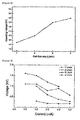
- FIG. 5 is a graph illustrating a discharge firing voltage according to a gas flow rate in the plasma jet device of FIG. 1 . Referring to FIG. 5 , it can be known that the discharge firing voltage of the plasma jet device increases when increasing the gas flow rate. The shorter time that the gas stays in an electric field, the high voltage required for discharge firing.
- FIG. 6 is a graph illustrating discharge voltage/current characteristics according to a gas flow rate in the plasma jet device of FIG. 1 .
- a discharge starts, a current rises and a voltage drops.
- a temperature was measured while jetting plasma to a thin aluminum layer for 10 minutes.
- the highest temperature of the jetted plasma was 41 °C. Since the time of processing plasma, required in bio-medical field, is 10 seconds or so, it is regarded as a thermal damage of a cell, caused by the plasma, does not occur.
- a device capable of jetting micro plasma under atmospheric pressure was manufactured. The manufactured device successfully jetted plasma under atmospheric pressure.
- the present invention may be applied to the field of bio-medical.
Landscapes
- Physics & Mathematics (AREA)
- Engineering & Computer Science (AREA)
- Plasma & Fusion (AREA)
- Chemical & Material Sciences (AREA)
- Analytical Chemistry (AREA)
- Spectroscopy & Molecular Physics (AREA)
- Plasma Technology (AREA)
- Surgical Instruments (AREA)
- Materials For Medical Uses (AREA)
- Coating By Spraying Or Casting (AREA)
Claims (17)
- Dispositif à micro-jets de plasma comprenant :une électrode (1) utilisée en tant qu'anode, dans lequel l'électrode est configurée pour expulser du plasma à travers des trous dans celle-ci ;un tuyau d'injection de gaz (5) injectant du gaz à partir de l'extérieur ; etune enveloppe isolante (3) ;caractérisé en ce que le tuyau d'injection de gaz (5) est utilisé en tant que cathode et en ce que le dispositif à micro-jets de plasma comprend en outre :un tube de protection (4) entourant le tuyau d'injection de gaz (5) pour protéger le tuyau d'injection de gaz (5) contre l'extérieur ; etun matériau isolant poreux (2) disposé entre ladite électrode (1) et le tuyau d'injection de gaz (5) et isolant l'électrode (1) du tuyau d'injection de gaz (5) et ayant une pluralité de trous de passage pour permettre au gaz injecté par le tuyau d'injection de gaz (5) d'être transféré dans l'électrode,dans lequel l'enveloppe isolante (3) entoure l'un de l'électrode (1), du matériau isolant poreux (2), et du tuyau d'injection de gaz (5), etdans lequel l'enveloppe isolante (3) est reliée au matériau isolant poreux (2) et empêche la diffusion d'une décharge se produisant entre l'électrode (1) et le tuyau d'injection de gaz (5) pour générer le plasma.
- Dispositif à micro-jets de plasma selon la revendication 1, dans lequel le tuyau d'injection de gaz (5) est constitué d'acier inoxydable.
- Dispositif à micro-jets de plasma selon la revendication 1, dans lequel le matériau isolant poreux (2) est constitué de céramique.
- Dispositif à micro-jets de plasma selon la revendication 3, dans lequel le matériau isolant poreux (2) est constitué d'alumine.
- Dispositif à micro-jets de plasma selon la revendication 1, dans lequel le tube de protection (4) est constitué de quartz.
- Procédé de fabrication d'une électrode (1) à utiliser dans un dispositif à micro-jets de plasma selon l'une quelconque des revendications 1 à 5,
caractérisé en ce que le procédé comprend :la formation d'une couche d'ensemencement sur une planche ;la formation d'une couche de moule sur la couche d'ensemencement ;la configuration de la couche de moule pour former une couche de moule configurée, dans lequel la couche de moule configurée comporte une pluralité de parties formant des trous d'électrode qui sont séparées l'une de l'autre ;la formation d'une couche d'électrode sur la planche où la couche de moule configurée est forméela planarisation de la couche de moule configurée et de la couche d'électrode ; etle retrait de la planche, de la couche d'ensemencement, et de la couche de moule configurée pour former l'électrode (1) qui comporte une pluralité de trous formés dans celle-ci, les trous correspondant aux parties formant des trous d'électrode. - Procédé selon la revendication 6, dans lequel, lors de la formation d'une couche d'ensemencement sur une planche, la couche d'ensemencement est formée par dépôt de titane/d'or jusqu'à une épaisseur de 500 Å et 2 500 Å.
- Procédé selon la revendication 7, dans lequel le titane/l'or est formé par un procédé de pulvérisation.
- Procédé selon la revendication 6, dans lequel, lors de la formation d'une couche de moule sur la couche d'ensemencement, la couche de moule est formée par revêtement avec un sensibilisateur négatif.
- Procédé selon la revendication 9, dans lequel l'épaisseur de la couche de moule est de 100 µm ou moins.
- Procédé selon la revendication 6, dans lequel, lors de la configuration de la couche de moule, la couche de moule est configurée de telle manière que chacune de la pluralité de parties formant des trous d'électrode est disposée de manière à être séparée l'une de l'autre par le même intervalle.
- Procédé selon la revendication 11, dans lequel la largeur des parties formant des trous d'électrode est de 100 µm ou moins.
- Procédé selon la revendication 6, dans lequel le nombre des parties formant des trous d'électrode générées est de 10 x 10 ou plus.
- Procédé selon la revendication 6, dans lequel, lors de la formation d'une couche d'électrode, la couche d'électrode est formée par revêtement métallique avec une couche de nickel.
- Procédé selon la revendication 14, dans lequel l'épaisseur de la couche de nickel formée sur les trous formant électrode est de 70 µm ou moins.
- Procédé selon la revendication 6, dans lequel, dans l'étape de planarisation de la couche de moule configurée et de la couche d'électrode, la couche de moule configurée et la couche d'électrode sont planarisées suivant un procédé de polissage mécano-chimique (CMP).
- Procédé selon la revendication 16, dans lequel l'épaisseur de la couche d'électrode planarisée est de 60 µm ou moins.
Applications Claiming Priority (3)
| Application Number | Priority Date | Filing Date | Title |
|---|---|---|---|
| KR20090016663 | 2009-02-27 | ||
| KR1020090028661A KR101001477B1 (ko) | 2009-02-27 | 2009-04-02 | 바이오-메디컬 응용을 위한 상압 저온 마이크로 플라즈마 분사 장치 |
| PCT/KR2009/005282 WO2010098524A1 (fr) | 2009-02-27 | 2009-09-17 | Dispositif atmosphérique à micro-jets de plasma à basse température pour application biomédicale |
Publications (3)
| Publication Number | Publication Date |
|---|---|
| EP2401896A1 EP2401896A1 (fr) | 2012-01-04 |
| EP2401896A4 EP2401896A4 (fr) | 2013-04-17 |
| EP2401896B1 true EP2401896B1 (fr) | 2015-10-21 |
Family
ID=43005262
Family Applications (1)
| Application Number | Title | Priority Date | Filing Date |
|---|---|---|---|
| EP09840870.1A Active EP2401896B1 (fr) | 2009-02-27 | 2009-09-17 | Dispositif à micro-jets de plasma atmosphérique à basse température pour application biomédicale |
Country Status (5)
| Country | Link |
|---|---|
| US (1) | US20110306924A1 (fr) |
| EP (1) | EP2401896B1 (fr) |
| JP (1) | JP5225476B2 (fr) |
| KR (1) | KR101001477B1 (fr) |
| WO (1) | WO2010098524A1 (fr) |
Families Citing this family (10)
| Publication number | Priority date | Publication date | Assignee | Title |
|---|---|---|---|---|
| KR101409390B1 (ko) * | 2012-02-29 | 2014-06-27 | 아주대학교산학협력단 | 바이오-메디컬 응용을 위해 플라즈마를 이용하는 질환세포 및 병원성 미생물의 사멸 방법 |
| KR101594464B1 (ko) * | 2013-10-02 | 2016-02-18 | 아주대학교산학협력단 | 마이크로 플라즈마 분사 소자, 적층형 마이크로 플라즈마 분사 모듈 및 마이크로 플라즈마 분사 소자의 제작 방법 |
| WO2015050376A1 (fr) * | 2013-10-02 | 2015-04-09 | 아주대학교산학협력단 | Élément de pulvérisation de microplasma, module de pulvérisation de microplasma stratifié et procédé de fabrication d'élément de pulvérisation de microplasma |
| CN103945630A (zh) * | 2014-04-21 | 2014-07-23 | 上海交通大学 | 无掩膜刻蚀聚合物薄膜的大气压空气微等离子体射流装置 |
| JP6651375B2 (ja) * | 2015-08-31 | 2020-02-19 | 積水化学工業株式会社 | プラズマ装置 |
| CN105744713B (zh) * | 2016-03-28 | 2018-10-23 | 大连民族大学 | 一种阵列针-板式液相等离子体射流发生装置 |
| US10328441B2 (en) | 2016-04-29 | 2019-06-25 | Semes Co., Ltd. | Nozzle unit and coating apparatus including the same |
| KR101830187B1 (ko) * | 2016-09-05 | 2018-02-21 | 아주대학교 산학협력단 | 저온 대기압 플라즈마 분사 장치 |
| US10433411B2 (en) | 2017-06-16 | 2019-10-01 | Sekisui Chemical Co., Ltd. | Plasma generating apparatus, therapeutic method, and method for activating cell or living tissue |
| CN109618481B (zh) * | 2018-12-14 | 2020-12-11 | 哈尔滨工业大学 | 低雷诺数条件的等离子体合成射流激励器 |
Citations (3)
| Publication number | Priority date | Publication date | Assignee | Title |
|---|---|---|---|---|
| WO2000079843A1 (fr) * | 1999-06-23 | 2000-12-28 | Skion Corporation | Appareil de traitement par gerbes de plasma produites par decharge d'electrodes capillaires |
| US6980629B1 (en) * | 2002-09-06 | 2005-12-27 | Siemens Aktiengesellschaft | Antiscatter grid or collimator, and a method of production |
| WO2007067924A2 (fr) * | 2005-12-07 | 2007-06-14 | Stryker Corporation | Système de stérilisation avec un générateur de plasma, le générateur de plasma comportant un ensemble d’électrodes comportant une matrice de capillaires dans lesquels le plasma est généré et dans lesquels du fluide est introduit |
Family Cites Families (18)
| Publication number | Priority date | Publication date | Assignee | Title |
|---|---|---|---|---|
| US4507181A (en) * | 1984-02-17 | 1985-03-26 | Energy Conversion Devices, Inc. | Method of electro-coating a semiconductor device |
| US5637539A (en) | 1996-01-16 | 1997-06-10 | Cornell Research Foundation, Inc. | Vacuum microelectronic devices with multiple planar electrodes |
| JP3328498B2 (ja) | 1996-02-16 | 2002-09-24 | 株式会社荏原製作所 | 高速原子線源 |
| US6116863A (en) * | 1997-05-30 | 2000-09-12 | University Of Cincinnati | Electromagnetically driven microactuated device and method of making the same |
| JPH11329334A (ja) * | 1998-05-20 | 1999-11-30 | Sanyo Electric Co Ltd | 半導体装置の製造方法 |
| JP2000068255A (ja) | 1998-08-21 | 2000-03-03 | Tokyo Electron Ltd | プラズマ用電極およびその製造方法 |
| US6890332B2 (en) * | 1999-05-24 | 2005-05-10 | Csaba Truckai | Electrical discharge devices and techniques for medical procedures |
| US6403286B1 (en) * | 1999-11-04 | 2002-06-11 | Corning Incorporated | High aspect ratio patterning of glass film |
| US6924401B2 (en) * | 2001-04-10 | 2005-08-02 | California Institute Of Technology | Plasma microjet arrays for selective oxidation of methane to methanol |
| EP1430501A2 (fr) * | 2001-07-02 | 2004-06-23 | Plasmasol Corporation | Electrode nouvelle a utiliser avec un appareil emetteur de plasma et son procede d'utilisation |
| DE10145131B4 (de) | 2001-09-07 | 2004-07-08 | Pva Tepla Ag | Vorrichtung zum Erzeugen eines Aktivgasstrahls |
| KR100837393B1 (ko) | 2002-01-22 | 2008-06-12 | 삼성에스디아이 주식회사 | 탄소와 친화도가 높은 금속을 전극으로 구비하는 전자소자 |
| KR100475074B1 (ko) * | 2002-05-16 | 2005-03-10 | 삼성전자주식회사 | 반도체 소자의 커패시터의 스토리지 전극 제조 방법 |
| KR100431581B1 (ko) * | 2002-05-28 | 2004-05-17 | 한국과학기술원 | 미소거울 구동기 |
| US7127301B1 (en) * | 2003-04-28 | 2006-10-24 | Sandia Corporation | Flexible retinal electrode array |
| US8521274B2 (en) * | 2005-04-25 | 2013-08-27 | Drexel University | Methods for non-thermal application of gas plasma to living tissue |
| JP4333883B2 (ja) * | 2007-01-24 | 2009-09-16 | ヤマハ株式会社 | モーションセンサ及びその製造方法 |
| US9283029B2 (en) * | 2007-01-31 | 2016-03-15 | Alma Lasers Ltd. | Skin treatment using a multi-discharge applicator |
-
2009
- 2009-04-02 KR KR1020090028661A patent/KR101001477B1/ko active Active
- 2009-09-17 WO PCT/KR2009/005282 patent/WO2010098524A1/fr not_active Ceased
- 2009-09-17 US US13/203,693 patent/US20110306924A1/en not_active Abandoned
- 2009-09-17 JP JP2011551973A patent/JP5225476B2/ja active Active
- 2009-09-17 EP EP09840870.1A patent/EP2401896B1/fr active Active
Patent Citations (3)
| Publication number | Priority date | Publication date | Assignee | Title |
|---|---|---|---|---|
| WO2000079843A1 (fr) * | 1999-06-23 | 2000-12-28 | Skion Corporation | Appareil de traitement par gerbes de plasma produites par decharge d'electrodes capillaires |
| US6980629B1 (en) * | 2002-09-06 | 2005-12-27 | Siemens Aktiengesellschaft | Antiscatter grid or collimator, and a method of production |
| WO2007067924A2 (fr) * | 2005-12-07 | 2007-06-14 | Stryker Corporation | Système de stérilisation avec un générateur de plasma, le générateur de plasma comportant un ensemble d’électrodes comportant une matrice de capillaires dans lesquels le plasma est généré et dans lesquels du fluide est introduit |
Also Published As
| Publication number | Publication date |
|---|---|
| WO2010098524A1 (fr) | 2010-09-02 |
| KR101001477B1 (ko) | 2010-12-14 |
| JP5225476B2 (ja) | 2013-07-03 |
| US20110306924A1 (en) | 2011-12-15 |
| EP2401896A1 (fr) | 2012-01-04 |
| EP2401896A4 (fr) | 2013-04-17 |
| JP2012519019A (ja) | 2012-08-23 |
| KR20100098256A (ko) | 2010-09-06 |
Similar Documents
| Publication | Publication Date | Title |
|---|---|---|
| EP2401896B1 (fr) | Dispositif à micro-jets de plasma atmosphérique à basse température pour application biomédicale | |
| US11427913B2 (en) | Method and apparatus for generating highly repetitive pulsed plasmas | |
| TWI374495B (fr) | ||
| US8916034B2 (en) | Thin-film forming sputtering system | |
| TW201139729A (en) | Method and device for layer deposition | |
| CN107546095B (zh) | 支撑组件、用于处理基底的装置和方法 | |
| TWI244124B (en) | Electronic device, its manufacturing method, and plasma processing apparatus | |
| TW201018320A (en) | In-chamber member temperature control method, in-chamber member, substrate mounting table and plasma processing apparatus including same | |
| KR101842127B1 (ko) | 기판 처리 장치 및 기판 처리 방법 | |
| EP3788181B1 (fr) | Procédé de génération de plasma à basse température, procédé de revêtement de tube électriquement conducteur ou ferromagnétique à l'aide d'un plasma pulsé et dispositifs correspondants | |
| CN113474482B (zh) | 用于事故耐受核燃料、粒子加速器、和航空航天前沿的金属和陶瓷纳米涂层的方法和设备 | |
| CN107833819A (zh) | 等离子体处理装置 | |
| WO2013099719A1 (fr) | Dispositif de traitement de substrat, procédé d'attaque chimique d'un film métallique et procédé de fabrication d'un élément magnétorésistif | |
| JP2011179119A (ja) | 熱拡散器を用いた物理蒸着装置及び方法 | |
| Kim et al. | A cold micro plasma jet device suitable for bio-medical applications | |
| US10224179B2 (en) | Ion beam processing apparatus, electrode assembly, and method of cleaning electrode assembly | |
| KR20130073844A (ko) | 내부식성 컴포넌트들을 갖는 플라즈마 처리 디바이스들 | |
| CN111801784A (zh) | 利用环形沿面放电等离子装置的点状蚀刻模块以及点状蚀刻模块的蚀刻轮廓的控制方法 | |
| KR101817210B1 (ko) | 플라즈마 발생 장치, 그를 포함하는 기판 처리 장치, 및 그 제어 방법 | |
| JP2012028273A (ja) | アース電極の接点及びその製造方法 | |
| KR101754563B1 (ko) | 이온 빔 생성 장치, 그를 이용한 기판 처리 장치, 및 이온 빔 제어 방법 | |
| KR101300966B1 (ko) | 기판도금장치 | |
| KR101585136B1 (ko) | 플라즈마 젯 표면처리 장치 및 그 분사노즐의 제조방법 | |
| KR101140502B1 (ko) | 중성화빔을 이용한 표면처리장치 | |
| KR100813694B1 (ko) | 플라즈마 포커스 장치 |
Legal Events
| Date | Code | Title | Description |
|---|---|---|---|
| PUAI | Public reference made under article 153(3) epc to a published international application that has entered the european phase |
Free format text: ORIGINAL CODE: 0009012 |
|
| 17P | Request for examination filed |
Effective date: 20110927 |
|
| AK | Designated contracting states |
Kind code of ref document: A1 Designated state(s): AT BE BG CH CY CZ DE DK EE ES FI FR GB GR HR HU IE IS IT LI LT LU LV MC MK MT NL NO PL PT RO SE SI SK SM TR |
|
| DAX | Request for extension of the european patent (deleted) | ||
| A4 | Supplementary search report drawn up and despatched |
Effective date: 20130318 |
|
| RIC1 | Information provided on ipc code assigned before grant |
Ipc: H05H 1/24 20060101AFI20130308BHEP Ipc: H01J 37/32 20060101ALI20130308BHEP |
|
| 17Q | First examination report despatched |
Effective date: 20140506 |
|
| GRAP | Despatch of communication of intention to grant a patent |
Free format text: ORIGINAL CODE: EPIDOSNIGR1 |
|
| INTG | Intention to grant announced |
Effective date: 20150504 |
|
| GRAS | Grant fee paid |
Free format text: ORIGINAL CODE: EPIDOSNIGR3 |
|
| GRAA | (expected) grant |
Free format text: ORIGINAL CODE: 0009210 |
|
| RAP1 | Party data changed (applicant data changed or rights of an application transferred) |
Owner name: AJOU UNIVERSITY INDUSTRY COOPERATION FOUNDATION |
|
| AK | Designated contracting states |
Kind code of ref document: B1 Designated state(s): AT BE BG CH CY CZ DE DK EE ES FI FR GB GR HR HU IE IS IT LI LT LU LV MC MK MT NL NO PL PT RO SE SI SK SM TR |
|
| REG | Reference to a national code |
Ref country code: GB Ref legal event code: FG4D Ref country code: NL Ref legal event code: MP Effective date: 20151021 |
|
| REG | Reference to a national code |
Ref country code: CH Ref legal event code: EP |
|
| REG | Reference to a national code |
Ref country code: AT Ref legal event code: REF Ref document number: 757386 Country of ref document: AT Kind code of ref document: T Effective date: 20151115 |
|
| REG | Reference to a national code |
Ref country code: IE Ref legal event code: FG4D |
|
| REG | Reference to a national code |
Ref country code: DE Ref legal event code: R096 Ref document number: 602009034422 Country of ref document: DE |
|
| REG | Reference to a national code |
Ref country code: LT Ref legal event code: MG4D |
|
| REG | Reference to a national code |
Ref country code: AT Ref legal event code: MK05 Ref document number: 757386 Country of ref document: AT Kind code of ref document: T Effective date: 20151021 |
|
| PG25 | Lapsed in a contracting state [announced via postgrant information from national office to epo] |
Ref country code: ES Free format text: LAPSE BECAUSE OF FAILURE TO SUBMIT A TRANSLATION OF THE DESCRIPTION OR TO PAY THE FEE WITHIN THE PRESCRIBED TIME-LIMIT Effective date: 20151021 Ref country code: NL Free format text: LAPSE BECAUSE OF FAILURE TO SUBMIT A TRANSLATION OF THE DESCRIPTION OR TO PAY THE FEE WITHIN THE PRESCRIBED TIME-LIMIT Effective date: 20151021 Ref country code: IT Free format text: LAPSE BECAUSE OF FAILURE TO SUBMIT A TRANSLATION OF THE DESCRIPTION OR TO PAY THE FEE WITHIN THE PRESCRIBED TIME-LIMIT Effective date: 20151021 Ref country code: LT Free format text: LAPSE BECAUSE OF FAILURE TO SUBMIT A TRANSLATION OF THE DESCRIPTION OR TO PAY THE FEE WITHIN THE PRESCRIBED TIME-LIMIT Effective date: 20151021 Ref country code: IS Free format text: LAPSE BECAUSE OF FAILURE TO SUBMIT A TRANSLATION OF THE DESCRIPTION OR TO PAY THE FEE WITHIN THE PRESCRIBED TIME-LIMIT Effective date: 20160221 Ref country code: HR Free format text: LAPSE BECAUSE OF FAILURE TO SUBMIT A TRANSLATION OF THE DESCRIPTION OR TO PAY THE FEE WITHIN THE PRESCRIBED TIME-LIMIT Effective date: 20151021 Ref country code: NO Free format text: LAPSE BECAUSE OF FAILURE TO SUBMIT A TRANSLATION OF THE DESCRIPTION OR TO PAY THE FEE WITHIN THE PRESCRIBED TIME-LIMIT Effective date: 20160121 |
|
| PG25 | Lapsed in a contracting state [announced via postgrant information from national office to epo] |
Ref country code: GR Free format text: LAPSE BECAUSE OF FAILURE TO SUBMIT A TRANSLATION OF THE DESCRIPTION OR TO PAY THE FEE WITHIN THE PRESCRIBED TIME-LIMIT Effective date: 20160122 Ref country code: SE Free format text: LAPSE BECAUSE OF FAILURE TO SUBMIT A TRANSLATION OF THE DESCRIPTION OR TO PAY THE FEE WITHIN THE PRESCRIBED TIME-LIMIT Effective date: 20151021 Ref country code: FI Free format text: LAPSE BECAUSE OF FAILURE TO SUBMIT A TRANSLATION OF THE DESCRIPTION OR TO PAY THE FEE WITHIN THE PRESCRIBED TIME-LIMIT Effective date: 20151021 Ref country code: AT Free format text: LAPSE BECAUSE OF FAILURE TO SUBMIT A TRANSLATION OF THE DESCRIPTION OR TO PAY THE FEE WITHIN THE PRESCRIBED TIME-LIMIT Effective date: 20151021 Ref country code: LV Free format text: LAPSE BECAUSE OF FAILURE TO SUBMIT A TRANSLATION OF THE DESCRIPTION OR TO PAY THE FEE WITHIN THE PRESCRIBED TIME-LIMIT Effective date: 20151021 Ref country code: PL Free format text: LAPSE BECAUSE OF FAILURE TO SUBMIT A TRANSLATION OF THE DESCRIPTION OR TO PAY THE FEE WITHIN THE PRESCRIBED TIME-LIMIT Effective date: 20151021 Ref country code: PT Free format text: LAPSE BECAUSE OF FAILURE TO SUBMIT A TRANSLATION OF THE DESCRIPTION OR TO PAY THE FEE WITHIN THE PRESCRIBED TIME-LIMIT Effective date: 20160222 |
|
| REG | Reference to a national code |
Ref country code: DE Ref legal event code: R097 Ref document number: 602009034422 Country of ref document: DE |
|
| PG25 | Lapsed in a contracting state [announced via postgrant information from national office to epo] |
Ref country code: CZ Free format text: LAPSE BECAUSE OF FAILURE TO SUBMIT A TRANSLATION OF THE DESCRIPTION OR TO PAY THE FEE WITHIN THE PRESCRIBED TIME-LIMIT Effective date: 20151021 |
|
| PLBE | No opposition filed within time limit |
Free format text: ORIGINAL CODE: 0009261 |
|
| STAA | Information on the status of an ep patent application or granted ep patent |
Free format text: STATUS: NO OPPOSITION FILED WITHIN TIME LIMIT |
|
| PG25 | Lapsed in a contracting state [announced via postgrant information from national office to epo] |
Ref country code: SK Free format text: LAPSE BECAUSE OF FAILURE TO SUBMIT A TRANSLATION OF THE DESCRIPTION OR TO PAY THE FEE WITHIN THE PRESCRIBED TIME-LIMIT Effective date: 20151021 Ref country code: DK Free format text: LAPSE BECAUSE OF FAILURE TO SUBMIT A TRANSLATION OF THE DESCRIPTION OR TO PAY THE FEE WITHIN THE PRESCRIBED TIME-LIMIT Effective date: 20151021 Ref country code: EE Free format text: LAPSE BECAUSE OF FAILURE TO SUBMIT A TRANSLATION OF THE DESCRIPTION OR TO PAY THE FEE WITHIN THE PRESCRIBED TIME-LIMIT Effective date: 20151021 Ref country code: SM Free format text: LAPSE BECAUSE OF FAILURE TO SUBMIT A TRANSLATION OF THE DESCRIPTION OR TO PAY THE FEE WITHIN THE PRESCRIBED TIME-LIMIT Effective date: 20151021 Ref country code: RO Free format text: LAPSE BECAUSE OF FAILURE TO SUBMIT A TRANSLATION OF THE DESCRIPTION OR TO PAY THE FEE WITHIN THE PRESCRIBED TIME-LIMIT Effective date: 20151021 |
|
| 26N | No opposition filed |
Effective date: 20160722 |
|
| PG25 | Lapsed in a contracting state [announced via postgrant information from national office to epo] |
Ref country code: SI Free format text: LAPSE BECAUSE OF FAILURE TO SUBMIT A TRANSLATION OF THE DESCRIPTION OR TO PAY THE FEE WITHIN THE PRESCRIBED TIME-LIMIT Effective date: 20151021 |
|
| PG25 | Lapsed in a contracting state [announced via postgrant information from national office to epo] |
Ref country code: BE Free format text: LAPSE BECAUSE OF FAILURE TO SUBMIT A TRANSLATION OF THE DESCRIPTION OR TO PAY THE FEE WITHIN THE PRESCRIBED TIME-LIMIT Effective date: 20151021 |
|
| PG25 | Lapsed in a contracting state [announced via postgrant information from national office to epo] |
Ref country code: MC Free format text: LAPSE BECAUSE OF FAILURE TO SUBMIT A TRANSLATION OF THE DESCRIPTION OR TO PAY THE FEE WITHIN THE PRESCRIBED TIME-LIMIT Effective date: 20151021 |
|
| REG | Reference to a national code |
Ref country code: CH Ref legal event code: PL |
|
| GBPC | Gb: european patent ceased through non-payment of renewal fee |
Effective date: 20160917 |
|
| REG | Reference to a national code |
Ref country code: IE Ref legal event code: MM4A |
|
| REG | Reference to a national code |
Ref country code: FR Ref legal event code: ST Effective date: 20170531 |
|
| PG25 | Lapsed in a contracting state [announced via postgrant information from national office to epo] |
Ref country code: LI Free format text: LAPSE BECAUSE OF NON-PAYMENT OF DUE FEES Effective date: 20160930 Ref country code: IE Free format text: LAPSE BECAUSE OF NON-PAYMENT OF DUE FEES Effective date: 20160917 Ref country code: FR Free format text: LAPSE BECAUSE OF NON-PAYMENT OF DUE FEES Effective date: 20160930 Ref country code: CH Free format text: LAPSE BECAUSE OF NON-PAYMENT OF DUE FEES Effective date: 20160930 Ref country code: GB Free format text: LAPSE BECAUSE OF NON-PAYMENT OF DUE FEES Effective date: 20160917 |
|
| PG25 | Lapsed in a contracting state [announced via postgrant information from national office to epo] |
Ref country code: LU Free format text: LAPSE BECAUSE OF NON-PAYMENT OF DUE FEES Effective date: 20160917 |
|
| PG25 | Lapsed in a contracting state [announced via postgrant information from national office to epo] |
Ref country code: CY Free format text: LAPSE BECAUSE OF FAILURE TO SUBMIT A TRANSLATION OF THE DESCRIPTION OR TO PAY THE FEE WITHIN THE PRESCRIBED TIME-LIMIT Effective date: 20151021 Ref country code: HU Free format text: LAPSE BECAUSE OF FAILURE TO SUBMIT A TRANSLATION OF THE DESCRIPTION OR TO PAY THE FEE WITHIN THE PRESCRIBED TIME-LIMIT; INVALID AB INITIO Effective date: 20090917 |
|
| PG25 | Lapsed in a contracting state [announced via postgrant information from national office to epo] |
Ref country code: TR Free format text: LAPSE BECAUSE OF FAILURE TO SUBMIT A TRANSLATION OF THE DESCRIPTION OR TO PAY THE FEE WITHIN THE PRESCRIBED TIME-LIMIT Effective date: 20151021 Ref country code: MK Free format text: LAPSE BECAUSE OF FAILURE TO SUBMIT A TRANSLATION OF THE DESCRIPTION OR TO PAY THE FEE WITHIN THE PRESCRIBED TIME-LIMIT Effective date: 20151021 Ref country code: MT Free format text: LAPSE BECAUSE OF NON-PAYMENT OF DUE FEES Effective date: 20160930 |
|
| PG25 | Lapsed in a contracting state [announced via postgrant information from national office to epo] |
Ref country code: BG Free format text: LAPSE BECAUSE OF FAILURE TO SUBMIT A TRANSLATION OF THE DESCRIPTION OR TO PAY THE FEE WITHIN THE PRESCRIBED TIME-LIMIT Effective date: 20151021 |
|
| PGFP | Annual fee paid to national office [announced via postgrant information from national office to epo] |
Ref country code: DE Payment date: 20250624 Year of fee payment: 17 |