EP2403059A1 - Ensemble d'antenne crantée pour dispositif mobile compact - Google Patents
Ensemble d'antenne crantée pour dispositif mobile compact Download PDFInfo
- Publication number
- EP2403059A1 EP2403059A1 EP10166657A EP10166657A EP2403059A1 EP 2403059 A1 EP2403059 A1 EP 2403059A1 EP 10166657 A EP10166657 A EP 10166657A EP 10166657 A EP10166657 A EP 10166657A EP 2403059 A1 EP2403059 A1 EP 2403059A1
- Authority
- EP
- European Patent Office
- Prior art keywords
- ground plane
- antenna
- notches
- antenna assembly
- edge
- Prior art date
- Legal status (The legal status is an assumption and is not a legal conclusion. Google has not performed a legal analysis and makes no representation as to the accuracy of the status listed.)
- Ceased
Links
- 230000005855 radiation Effects 0.000 claims abstract description 42
- 230000008878 coupling Effects 0.000 claims abstract description 6
- 238000010168 coupling process Methods 0.000 claims abstract description 6
- 238000005859 coupling reaction Methods 0.000 claims abstract description 6
- 238000004891 communication Methods 0.000 claims description 19
- 239000000758 substrate Substances 0.000 claims description 15
- 238000010295 mobile communication Methods 0.000 description 25
- 238000000034 method Methods 0.000 description 7
- 230000001413 cellular effect Effects 0.000 description 4
- 239000004020 conductor Substances 0.000 description 3
- 238000005516 engineering process Methods 0.000 description 3
- 230000006870 function Effects 0.000 description 3
- 239000000463 material Substances 0.000 description 3
- RYGMFSIKBFXOCR-UHFFFAOYSA-N Copper Chemical compound [Cu] RYGMFSIKBFXOCR-UHFFFAOYSA-N 0.000 description 2
- 239000003570 air Substances 0.000 description 2
- 238000013459 approach Methods 0.000 description 2
- 239000000919 ceramic Substances 0.000 description 2
- 229910052802 copper Inorganic materials 0.000 description 2
- 239000010949 copper Substances 0.000 description 2
- 238000010586 diagram Methods 0.000 description 2
- 239000011152 fibreglass Substances 0.000 description 2
- 230000005404 monopole Effects 0.000 description 2
- 239000004033 plastic Substances 0.000 description 2
- 239000000853 adhesive Substances 0.000 description 1
- 230000001070 adhesive effect Effects 0.000 description 1
- 230000004075 alteration Effects 0.000 description 1
- 239000011230 binding agent Substances 0.000 description 1
- 239000003990 capacitor Substances 0.000 description 1
- 230000015556 catabolic process Effects 0.000 description 1
- 230000008859 change Effects 0.000 description 1
- 230000007423 decrease Effects 0.000 description 1
- 230000003247 decreasing effect Effects 0.000 description 1
- 238000006731 degradation reaction Methods 0.000 description 1
- 238000013461 design Methods 0.000 description 1
- 230000000694 effects Effects 0.000 description 1
- 239000003822 epoxy resin Substances 0.000 description 1
- 238000005530 etching Methods 0.000 description 1
- 239000000446 fuel Substances 0.000 description 1
- 230000001939 inductive effect Effects 0.000 description 1
- 230000003993 interaction Effects 0.000 description 1
- 230000007246 mechanism Effects 0.000 description 1
- 239000002184 metal Substances 0.000 description 1
- 229910052751 metal Inorganic materials 0.000 description 1
- 238000012986 modification Methods 0.000 description 1
- 230000004048 modification Effects 0.000 description 1
- 229920000647 polyepoxide Polymers 0.000 description 1
- 238000003825 pressing Methods 0.000 description 1
- 230000008569 process Effects 0.000 description 1
- 230000009467 reduction Effects 0.000 description 1
- 238000005476 soldering Methods 0.000 description 1
- 238000006467 substitution reaction Methods 0.000 description 1
- 239000002759 woven fabric Substances 0.000 description 1
Images




Classifications
-
- H—ELECTRICITY
- H01—ELECTRIC ELEMENTS
- H01Q—ANTENNAS, i.e. RADIO AERIALS
- H01Q1/00—Details of, or arrangements associated with, antennas
- H01Q1/48—Earthing means; Earth screens; Counterpoises
-
- H—ELECTRICITY
- H01—ELECTRIC ELEMENTS
- H01Q—ANTENNAS, i.e. RADIO AERIALS
- H01Q1/00—Details of, or arrangements associated with, antennas
- H01Q1/12—Supports; Mounting means
- H01Q1/22—Supports; Mounting means by structural association with other equipment or articles
- H01Q1/24—Supports; Mounting means by structural association with other equipment or articles with receiving set
- H01Q1/241—Supports; Mounting means by structural association with other equipment or articles with receiving set used in mobile communications, e.g. GSM
- H01Q1/242—Supports; Mounting means by structural association with other equipment or articles with receiving set used in mobile communications, e.g. GSM specially adapted for hand-held use
- H01Q1/243—Supports; Mounting means by structural association with other equipment or articles with receiving set used in mobile communications, e.g. GSM specially adapted for hand-held use with built-in antennas
-
- H—ELECTRICITY
- H01—ELECTRIC ELEMENTS
- H01Q—ANTENNAS, i.e. RADIO AERIALS
- H01Q5/00—Arrangements for simultaneous operation of antennas on two or more different wavebands, e.g. dual-band or multi-band arrangements
Definitions
- This disclosure relates to an antenna assembly for a mobile wireless communications device, and more specifically to an antenna assembly that includes a ground plane configured with a plurality of notches that increase the electrical length of the ground plane without inducing radiation within the notched areas.
- the length of the ground plane or chassis in a wireless communications device affects the antenna operating frequency.
- an optimum performance of an antenna may be achieved when the physical length of the ground plane is half of a wavelength at the operating frequency or ⁇ 2.
- GHz Gigahertz
- A would be equal to approximately 15.4 centimeters (cm), which would require that the length of the ground plane be about 7.7 cm for optimum performance.
- MHz Megahertz
- A would be equal to about 33.4 cm, which would require that the length of the ground plane be about 16.7 cm for optimum performance.
- achieving the best performance requires that the length of the chassis or ground plane of the wireless device increase beyond a typical mobile phone chassis or ground plane of approximately 10.5 centimeters.
- GSM Global System for Mobile Communications
- MHz Megahertz
- 900 MHZ a ground plane of a wireless device
- an extension of the length of the chassis or ground plane of the typical mobile wireless device would be required.
- Such an elongated chassis may not be desirable or acceptable, especially in cases where a compact or small mobile device is desired.
- FIG. 1 illustrates a planar isometric view of the notched antenna assembly in a mobile wireless communication device in accordance with an illustrative embodiment of the disclosure
- FIG. 2 illustrates a block diagram of the wireless mobile communications systems according to an illustrative embodiment of the disclosure
- FIG. 3 illustrates a planar view of a notched antenna assembly in accordance with an illustrative embodiment of the disclosure
- FIG. 4A illustrates the current distribution of the notched antenna assembly illustrated in FIG. 3 at a frequency at the 900 MHz band in accordance with an illustrative embodiment of the disclosure
- FIG. 4B illustrates the current distribution of the notched antenna assembly illustrated in FIG. 3 at a frequency at the 1880 MHz band in accordance with an illustrative embodiment of the disclosure
- FIG. 5A illustrates a two-dimensional plot of the radiation pattern of the notched antenna assembly illustrated in FIG. 3 in the phi plane at 900 MHZ band;
- FIG. 5B illustrates a two-dimensional plot of the radiation pattern of the notched antenna assembly illustrated in FIG. 3 in the theta plane at 900 MHz band;
- FIG. 5C illustrates a two-dimensional plot of the radiation pattern of the notched antenna assembly illustrated in FIG. 3 in the phi plane at 1880 MHZ band;
- FIG. 5D illustrates a two-dimensional plot of the radiation pattern of the notched antenna assembly illustrated in FIG. 3 in the theta plane at 1880 MHZ band;
- FIG. 6 illustrates a planar view of a notched antenna assembly in accordance with an illustrative embodiment of the disclosure
- FIG. 7A illustrates the current distribution on the ground plane illustrated in FIG. 6 at a frequency at 900 MHz band in accordance with an illustrative embodiment of the disclosure
- FIG. 7B illustrates the current distribution on the ground plane illustrated in FIG. 6 at a frequency at 1880 MHz band in accordance with an illustrative embodiment of the disclosure
- FIG. 8A illustrates a two-dimensional plot of the radiation pattern of the notched antenna assembly illustrated in FIG. 6 in the phi plane at 900 MHZ band;
- FIG. 8B illustrates a two-dimensional plot of the radiation pattern of the notched antenna assembly illustrated in FIG. 6 in the theta plane at 900 MHZ band;
- FIG. 8C illustrates a two-dimensional plot of the radiation pattern of the notched antenna assembly illustrated in FIG. 6 in the phi plane at 1880 MHZ band;
- FIG. 8D illustrates a two-dimensional plot of the radiation pattern of the notched antenna assembly illustrated in FIG. 6 in the theta plane at 1880 MHZ band.
- FIG. 9 illustrates an antenna of the notched antenna assembly of FIG. 1 in accordance with an illustrative embodiment of the disclosure.
- an antenna assembly for a wireless communications device comprises a single ground plane having a plurality of notches spaced apart at a distance from each other along at least two opposing longitudinal edges of the ground plane. Each notch of the plurality of notches is dimensioned to eliminate radiation from the individual notches.
- the antenna assembly also comprises a single antenna disposed at an edge of the ground plane that is perpendicular to a first opposing longitudinal edge and a second opposing longitudinal edge of said at least two opposing edges.
- the plurality of notches are positioned at a distance that prevents radiative coupling with said single antenna.
- a mobile communications device comprises a single ground plane having a plurality of notches spaced apart at a distance from each other and disposed along at least two opposing edges of said ground plane, wherein said plurality of notches are individually non-radiating.
- the mobile communications device includes a single antenna disposed at an edge of said single ground plane that is perpendicular to a first opposing longitudinal edge and a second opposing longitudinal edge of said at least two opposing edges, said single antenna being positioned at a distance that prevents radiative coupling with said plurality of notches.
- the singular antenna indices current on the singular ground plane.
- the present disclosure provides a chassis or ground plane of an antenna assembly in a mobile communications device.
- the ground plane of the antenna assembly comprises a plurality of notches etched or cut into edges of the ground plane that are opposite to the edge on which the antenna is disposed.
- the notches control the frequency at which the ground plane resonates and may be dimensioned so that the ground plane resonates concurrently or at approximately the same time as the antenna at a designated frequency.
- the best performance of an antenna, as indicated by increased bandwidth and total efficiency, in a mobile communications device may be achieved when both the combination of the chassis or ground plane and the antenna resonate at the same time.
- the ground plane and the antenna may resonate at the same time as the physical length of the ground plane approaches about 17.0 cm.
- high frequency bands about or exceeding 1 GHz such as, but not limited to 1.9 GHz, the ground plane and the antenna may resonate at the same time as the ground plane approaches a length of approximately 8.0 cm.
- the notches increase the electrical length of the ground plane without any corresponding increase in the physical length of the ground plane by forcing the surface currents induced on the ground plane by the antenna to travel a distance that is greater than the linear distance along the perimeter of the ground plane without the notches.
- the notches are sized to have a trace that is electrically small to prevent each notch from radiating at any frequency and operating as individual antennas.
- the notches may all be of rectangular dimensions, square dimensions, or a combination of rectangular and square dimensions. The dimensions of the notches prevent the notches from radiating or acting as a source of radiation within the ground plane.
- FIG. 1 an isometric planar view of an antenna assembly 104 in a mobile communications device 100 is depicted in accordance with an illustrative embodiment of the disclosure.
- Antenna assembly 104 includes single antenna 106 mounted on a first edge of a single ground plane 120 that is contiguous in shape.
- Antenna assembly 104 is disposed or located within a housing 102 for mobile communication device 100 or similar mobile terminal.
- a number of components may be mounted anywhere on the entire surface area of either side of ground plane 120.
- the components may include, without limitation, audio output transducer 108, auxiliary I/O device 110 , primary circuitry 112 , radio frequency circuitry 114, battery 116 , and audio output transducer 118.
- the components may include passive elements, such as capacitors (not shown), and resistors (not shown), and active elements, such as integrated circuit chips.
- the components may be mounted to ground plane 120 through vias, traces, pads, and other such mounting techniques recognized by one skilled in the art.
- Ground plane 120 of antenna assembly 104 is a single contiguous piece of conductive material.
- the conductive material may be a metal such as copper or other material known in the art for having good conducting properties. It must be noted that the number of components arranged and illustrated on ground plane 120 is not limited to the number or arrangement of components depicted in antenna assembly 104.
- Wireless mobile communications system 200 depicts an implementation of a mobile communication device, such as mobile communication device 100 of FIG. 1 .
- mobile communication device 204 may be a mobile wireless communication device, such as a mobile cellular device, herein referred to as a mobile device that may function as a Smartphone, which may be configured according to an information technology (IT) policy.
- Mobile communication device 204 may be configured with a notched antenna assembly, such as notched antenna assembly 104 of FIG. 1 .
- Examples of applicable communication devices include pagers, mobile cellular phones, cellular smart-phones, wireless organizers, personal digital assistants, computers, laptops, handheld wireless communication devices, wirelessly enabled notebook computers and such other communication devices.
- the mobile communication device 204 is a two-way communication device with advanced data communication capabilities including the capability to communicate with other mobile devices, computer systems, and assistants through a network of transceivers.
- the mobile communication device includes a number of components such as microprocessor 230 that control the overall operation of mobile communication device 204.
- Radio frequency circuit 210 includes wireless signal receiver 212 and wireless signal transmitter 218 connected to multi-element antenna assembly 206. Radio frequency circuit 210 may also include digital signal processor (DSP) 214 and local oscillators (LOS) 216. The specific design and implementation of radio frequency circuit 210 depends on the communication network in which mobile communication device 204 operates. Mobile communication device 204 receives messages from and sends messages across wireless communications network 202.
- DSP digital signal processor
- LOS local oscillators
- Mobile communication device 204 includes battery 208 for supplying power to the internal components.
- the battery 208 can be a smart battery with an embedded microprocessor.
- the battery 208 is coupled to a regulator (not shown), which assists the battery 208 in providing power V+ to the mobile communication device 204.
- a regulator not shown
- future technologies such as micro fuel cells may provide the power to the mobile communication device 204.
- Primary circuitry such as primary circuitry 112 of FIG. 1 , includes microprocessor 230, memory that includes a random access memory (RAM) 240, and a flash memory 238 which provides non-volatile storage.
- Serial port 232 constitutes a mechanism by which external devices, such as a personal computer, may be connected to mobile communication device 204.
- Display 236 and keyboard 234 provide a user interface for controlling mobile communication device 204.
- Audio input device 226 and audio output device 224 connect to primary circuitry 220 to function as an audio interface.
- a received signal such as a text message, an e-mail message, or web page download will be processed by the radio frequency circuit 210 and input to the microprocessor 230.
- the microprocessor 230 will then process the received signal for output to the display 236 or alternatively to the auxiliary I/O subsystem 228.
- a subscriber may also compose data items, such as e-mail messages, for example, using the keyboard 234 in conjunction with the display 236 and possibly the auxiliary I/O subsystem 228.
- the auxiliary I/O subsystem 228 may include devices such as: a touch screen, mouse, track ball, infrared fingerprint detector, or a roller wheel with dynamic button pressing capability.
- the keyboard 234 is preferably an alphanumeric keyboard together with or without a telephone-type keypad. However, other types of keyboards may also be used.
- FIG. 3 illustrates a top planar view of antenna assembly 300 in accordance with an illustrative embodiment of the disclosure.
- antenna assembly 300 may be antenna assembly 104 as illustrated in FIG. 1 .
- antenna 310 is shown disposed on a first edge 304 of ground plane 320.
- Ground plane 320 has a plurality of notches 312 extending in a longitudinal direction along a second edge 302 that is opposite to and perpendicular to the plane of antenna 310 and to first edge 304.
- Third edge 306 has a plurality of notches 314 extending in a longitudinal direction perpendicular to the plane of antenna 310 and opposite first edge 304 and second edge 302.
- a fourth edge 308 may also include a number of notches.
- Dielectric substrate 330 is disposed on an opposite side of ground plane 320 and may be configured with a pattern of a plurality of notches that is substantially the same as the pattern of plurality of notches, such as plurality of notches 312, 314, in ground plane 320.
- Dielectric substrate 330 may be formed from a material that includes, but is in no way limited to, air, fiberglass, plastic, and ceramic. Circuit board components may be placed on ground plane 320 or on dielectric substrate 330 through the connection of signal traces to the ground plane 320.
- the plurality of notches may approximate the shape of a square waveform having a plurality of pulses that are uniformly disposed along first edge 304 and third edge 306 of ground plane 320 at a distance d 322 from antenna 310.
- Distance d 322 is the smallest distance required to prevent electromagnetic interaction or radiative coupling between antenna 310 and a first notch of plurality of notches 312 and 314 disposed on either edge 304 and 30. ln illustrative embodiments of this disclosure, distance d 322 is approximately one centimeter. In alternate embodiments, distance d 322 should be no larger than lambda/10 or ⁇ 10.
- each edge of the pulse or the height 318 and width 316 of each pulse may be approximately 5 millimeters (mm).
- the plurality of notches may approximate the shape of a rectangular wave where the height of a pulse of the waveform is approximately 8 mm and much less than lambda/10 or ⁇ 10 , and the width of the pulse of the waveform is approximately 5 mm. In another embodiment, the plurality of notches may approximate the shape of a waveform that comprises a combination of square pulses and rectangular pulses.
- Antenna 310 may be, but is in no way limited to, a planar inverted F antenna (PIFA), an inverted F antenna (IFA), a type of monopole antenna, and a three dimensional antenna comprised of a plurality of strip segments joined together.
- antenna 310 may be a three-dimensional conductive U-shaped monopole structure.
- antenna 310 may be a hex-band antenna.
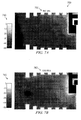
- FIG. 4A and FIG. 4B the current distribution 400 of the notched antenna assembly 300 of FIG. 3 is illustrated at selected resonant frequencies.
- the notches of antenna assembly 300 are designed to produce a resonance in the ground plane at the same frequency at which the antenna resonates.
- the notches are used to control the electrical length of the ground plane to enable both the ground plane and the antenna to resonate at the same time.
- Antenna performance such as greater efficiency and increased bandwidth, is improved when the ground plane and the antenna resonate together.
- FIG. 4A illustrates current distribution 450 of the notched antenna assembly 300 illustrated in FIG, 3 at a frequency at the 900 MHz band in accordance with an illustrative embodiment of the disclosure.
- Scale 440 provides information in decibels (dB) on the strength of the radiation by a light to dark gradation of shading. Scale 440 starts with a light gradation at 0 dB to represent a high current intensity and radiation level and decreases significantly through 50 dB represented by a darker gradation which represents decreased current intensity and radiation.
- dB decibels
- FIG. 4A illustrates the path the current travels along the length of the ground plane at a resonant frequency at 900 MHZ band.
- the total distance traveled by the current in a longitudinal direction along the ground plane includes the distance the current travels along the perimeter of each notch along the edge of the ground plane.
- FIG. 4B illustrates the current distribution 460 of the notched antenna assembly 300 illustrated in FIG. 3 at a frequency of 1880 MHz in accordance with an illustrative embodiment of the disclosure.
- Scale 440 provides information in decibels (dB) on the strength of the radiation through a light to dark gradation of shading, where lighter areas of the scale represent the greater current intensity and greater radiation.
- the distance from the antenna that includes the notched edges of the ground plane is greater than a linear distance from the antenna without the notches in the ground plane.
- FIG. 4B illustrates the path the current travels along the length of the ground plane at the resonant frequency of 1880 MHZ.
- FIG. 4B illustrates that the current induced by the antenna at the resonant frequency of 1880 MHZ, travels a longer distance along the notched edges of the ground plane.
- the total distance traveled by the current in a longitudinal direction along the ground plane includes the distance the current travels along the perimeter of each notch along the edge of the ground plane.
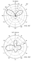
- FIG. 5A through FIG. 5D illustrate two-dimensional plots 500 of the radiation pattern of notched antenna assembly 300 at frequency bands of 900 MHZ and 1880 MHz.
- the dimensions and number of notches do not affect the radiation characteristics of the antenna.
- two-dimensional plot 500 illustrates the radiation pattern of the notched antenna assembly 300 illustrated in FIG. 3 .
- Polar plot 520 illustrates the far field radiation pattern in the phi plane for the notched antenna assembly with the ground plane current distribution characteristic of FIG. 4A at a frequency band at 900 MHz.
- two-dimensional plot 500 illustrates a polar plot 530 of the far field radiation pattern in the theta plane for the notched antenna assembly with the ground plane current distribution characteristic illustrated in FIG. 4A for a frequency band at 900 MHz.
- FIG. 5C illustrates polar plot 540 in the phi plane for the notched antenna assembly illustrated in FIG. 4B for a frequency of 1880 MHz.
- two-dimensional plot 500 illustrates a polar plot 550 of the far field radiation pattern in the theta plane for the notched antenna assembly illustrated in FIG. 4B at a frequency of 1880 MHZ.
- antenna 610 is shown disposed on a first edge 604 of ground plane 620.
- Ground plane 620 has a plurality of notches 612 extending in a longitudinal direction along a second edge 602 that is opposite to and perpendicular to the plane of antenna 610 and to first edge 604.
- Third edge 606 has a plurality of notches 614 extending in a longitudinal direction perpendicular to the plane of antenna 610 and opposite first edge 604 and second edge 602.
- a fourth edge 608 may also include a number of notches.
- Dielectric substrate 630 is disposed on an opposite side of ground plane 620 and may be configured with a pattern of a plurality of notches that is substantially the same as the pattern of plurality of notches, such as plurality of notches 612, 614, in ground plane 620.
- Circuit board components may be placed on ground plane 620 or on dielectric substrate 630 through the connection of signal traces to the ground plane 620.
- the plurality of notches, 612 and 614 may approximate the shape of a waveform or a series of undulating waveforms with a plurality of pulses having scalloped or substantially linear edges that are uniformly disposed along each edge of the ground plane at a distance d 622 from antenna 610.
- Each pulse may approximate the shape of a rectangle or square.
- Each pulse of the waveform may be non-uniform in height and width.
- the height 618 of a pulse may be 8mm and the width 616 of each pulse may be approximately 5 millimeters (mm).
- the plurality of notches 612 are used to control the electrical length of the ground plane to enable both the ground plane and the antenna to resonate at the same time. Antenna performance, such as greater efficiency and increased bandwidth, is improved when the ground plane and the antenna resonate together.
- Scale 740 provides information in decibels (dB) on the strength of the radiation through a light to dark gradation of shading, where lighter areas of the scale represent the greater current intensity and greater radiation.
- the distance from the antenna that includes the notched edges of the ground plane is greater than a linear distance from the antenna without the notches in the ground plane.
- FIG. 7A illustrates that the current distribution 750 induced by antenna assembly 600 at a resonant frequency band of 900 MHz travels a certain distance along each notch along the edges of the ground plane.
- the illustrative embodiments of FIG. 4A and FIG. 7A illustrate that the radiation characteristics of the resonating antenna assembly, 300 and 600 respectively, are not affected by the number or pattern of the notches of the ground plane.
- antenna assembly 600 has a non-uniform pattern of notches along the edges of the ground plane.
- the current distribution 700 produced by this non-uniform pattern of notches at the resonant frequency at 900 MHz band is the same as the current distribution 400 produced by antenna assembly 300 with a uniform pattern of notches along the edges of the ground plane at the resonant frequency band of 900 MHz.
- FIG. 7B the current distribution 760 at the resonant frequency of 1880MHz of antenna assembly 600 of FIG. 6 is illustrated, according to an embodiment of the disclosure is illustrated.
- FIG. 7B illustrates that the current induced by the antenna at the resonant frequency of 1880 MHz, travels a longer distance in a longitudinal direction along the notched edges of the ground plane.
- the radiation pattern produced by antenna assembly 600 at 1880 MHz is not affected by the number or pattern of the notches in the ground plane.
- FIG. 8A through FIG. 8D illustrate two-dimensional plots 800 of the antenna radiation pattern at frequency bands of 900 MHZ and 1800 MHz.
- the far field radiation patterns for antenna assembly 600 illustrated by FIG. 8A through FIG . 8D are similar to the far field radiation patterns generated by antenna assembly 300 as illustrated by FIG. 5A through FIG. 5D .
- the similarity of the far field radiation patterns in FIG. 8A through FIG. 8D and FIG. 5A through FIG. 5D illustrates that the number and size of the notches in an antenna assembly, such as in the illustrative examples of antenna assembly 300 and antenna assembly 600, have no effect on the radiation characteristics of each respective antenna.
- FIG. 8A illustrates polar plot 820 that depicts the far field radiation pattern of antenna assembly 600 with the ground plane current distribution characteristic of FIG. 7A in the phi plane at a frequency band of 900 MHz.
- Polar plot 820 has approximately the same radiation pattern illustrated by polar plot 520 for notched antenna assembly 300.
- FIG. 8B illustrates polar plot 830 in the theta plane for notched antenna assembly 600 of FIG. 6 .
- Polar plot 830 depicts the far field radiation pattern of antenna 610 with the ground plane current distribution characteristic of FIG. 7A in the theta plane at a frequency of 900MHz.
- Polar plot 830 has approximately the same radiation pattern illustrated by plot 530 for notched antenna assembly 300.
- FIG. 8C illustrates polar plot 840 in the phi plane at a frequency of 1880 MHz for notched antenna assembly 600 of FIG. 6 .
- Polar plot 840 depicts the far field radiation pattern of antenna 610 with the ground plane current distribution characteristic of FIG. 7 B.
- Polar plot 840 has approximately the same radiation pattern illustrated by polar plot 540 of FIG. 5C for notched antenna assembly 300.
- FIG. 8D illustrates polar plot 850 in the theta plane for notched antenna assembly 600 of FIG. 6 .
- Polar plot 850 depicts the far field radiation pattern of antenna assembly 600 with the ground plane current distribution characteristic of FIG. 7B in the theta plane at a frequency of 1880 MHz.
- Polar plot 850 has approximately the same radiation pattern illustrated by plot 550 of FIG. 5D for notched antenna assembly 300.
- the radiation efficiency of the notched antenna assembly is increased over an antenna assembly that is not notched,
- 1 GHz such as, without limitation, 900 MHz
- notched antenna assembly 300 and notched antenna assembly 600 provides at least a 3% increase in efficiency over an antenna assembly that does not include notches.
- high frequency bands above 1 GHz such as, without limitation, 1880 MHz or 1.9 GHz
- the efficiency either remains unchanged or increases over an antenna assembly that does not include notches.
- notched antenna assembly 300 and notched antenna assembly 600 may provide up to a 22% increase in bandwidth over an antenna assembly that does not include notches.
- high frequency bands above 1 GHz such as, without limitation, 1880 MHz or 1.9 GHz, there is a positive percentage change in bandwidth over an antenna assembly that does not include notches.
- FIG. 9 illustrates an antenna of the notched antenna assembly in accordance with an illustrative embodiment of the disclosure.
- Antenna 920 may be antenna 106 of notched antenna assembly 104 illustrated in FIG. 1 .
- Antenna 920 may comprise individual electrically conductive strip segments, such as, without limitation, strip segment 920a, 920b, 920c, 920d, and 920e, connected together on a dielectric substrate 910.
- Dielectric substrate 910 may be a polyhedron that is rectangular in shape and have a plurality of surfaces.
- Antenna 920 includes a signal feed 930 that connects directly to one or more conductive strip segments, such as strip segment 920f.
- the strip segments may be connected to surfaces of dielectric substrate 910 by soldering, etching, or some other connective or adhesive means known to one skilled in the art.
- the strip segments may be formed from copper or some other conductive material known to one skilled in the art.
- Dielectric substrate 910 may be formed from a material that includes, but is in no way limited to, air, fiberglass, plastic, and ceramic.
- dielectric substrate 910 may be formed from an FR-4 laminate that is a continuous glass-woven fabric reinforced with an epoxy resin binder.
- antenna 920 may be configured for operation in multiple frequency bands.
- antenna 920 may operate as a hex-band antenna that resonates in a plurality of different operating frequency bands including, but in no way limited to, the Global System for Mobile communications (GSM) 900 MHz frequency band, the Digital Cellular System (DCS) frequency band, and the Universal Mobile Telecommunications System (UMTS) 2100 MHz band.
- GSM Global System for Mobile communications
- DCS Digital Cellular System
- UMTS Universal Mobile Telecommunications System
Landscapes
- Engineering & Computer Science (AREA)
- Computer Networks & Wireless Communication (AREA)
- Waveguide Aerials (AREA)
- Support Of Aerials (AREA)
Priority Applications (4)
| Application Number | Priority Date | Filing Date | Title |
|---|---|---|---|
| EP10166657A EP2403059A1 (fr) | 2010-06-21 | 2010-06-21 | Ensemble d'antenne crantée pour dispositif mobile compact |
| US12/820,843 US20110309992A1 (en) | 2010-06-21 | 2010-06-22 | Notched antenna assembly for compact mobile device |
| PCT/CA2011/050368 WO2011160223A1 (fr) | 2010-06-21 | 2011-06-17 | Ensemble antenne à encoches pour dispositif mobile compact |
| CN2011800307635A CN103038941A (zh) | 2010-06-21 | 2011-06-17 | 用于紧凑式移动设备的开槽天线组件 |
Applications Claiming Priority (1)
| Application Number | Priority Date | Filing Date | Title |
|---|---|---|---|
| EP10166657A EP2403059A1 (fr) | 2010-06-21 | 2010-06-21 | Ensemble d'antenne crantée pour dispositif mobile compact |
Publications (1)
| Publication Number | Publication Date |
|---|---|
| EP2403059A1 true EP2403059A1 (fr) | 2012-01-04 |
Family
ID=43242212
Family Applications (1)
| Application Number | Title | Priority Date | Filing Date |
|---|---|---|---|
| EP10166657A Ceased EP2403059A1 (fr) | 2010-06-21 | 2010-06-21 | Ensemble d'antenne crantée pour dispositif mobile compact |
Country Status (4)
| Country | Link |
|---|---|
| US (1) | US20110309992A1 (fr) |
| EP (1) | EP2403059A1 (fr) |
| CN (1) | CN103038941A (fr) |
| WO (1) | WO2011160223A1 (fr) |
Families Citing this family (8)
| Publication number | Priority date | Publication date | Assignee | Title |
|---|---|---|---|---|
| US9077069B2 (en) | 2012-10-09 | 2015-07-07 | Blackberry Limited | Method and apparatus for tunable antenna and ground plane for handset applications |
| TW201424124A (zh) * | 2012-12-12 | 2014-06-16 | Realtek Semiconductor Corp | 電流阻斷器及具有電流阻斷器的無線通訊裝置 |
| US9525207B2 (en) * | 2013-07-18 | 2016-12-20 | Adant Technologies, Inc. | Reconfigurable antenna structure with parasitic elements |
| EP4173663B1 (fr) | 2013-12-17 | 2025-09-03 | ResMed Pty Ltd | Appareil apte à être utilisé dans le traitement des maladies respiratoires |
| JP6638550B2 (ja) * | 2016-05-06 | 2020-01-29 | 株式会社デンソーウェーブ | 無線装置 |
| CN106571525B (zh) | 2016-11-10 | 2020-10-27 | 捷开通讯(深圳)有限公司 | 一种优化隔离度的天线系统及移动终端 |
| EP3897798B1 (fr) | 2018-12-18 | 2024-06-19 | ResMed Pty Ltd | Réservoir d'humidificateur |
| CN111525237B (zh) * | 2020-04-30 | 2021-08-13 | 维沃移动通信有限公司 | 双天线解耦结构及电子设备 |
Citations (5)
| Publication number | Priority date | Publication date | Assignee | Title |
|---|---|---|---|---|
| JP2004200936A (ja) * | 2002-12-17 | 2004-07-15 | Nec Corp | 携帯無線機及びアンテナ基板 |
| GB2439110A (en) * | 2006-06-13 | 2007-12-19 | Thales Holdings Uk Plc | Printed ultra-wideband antenna with reduced aperture clutter |
| US20080211725A1 (en) * | 2005-04-15 | 2008-09-04 | Nokia Corporation | Antenna having a plurality of resonant frequencies |
| US20090051597A1 (en) * | 2007-08-23 | 2009-02-26 | Research In Motion Limited | Antenna, and associated method, for a multi-band radio device |
| GB2453778A (en) * | 2007-10-18 | 2009-04-22 | Thales Holdings Uk Plc | An ultra wideband antenna with a high impedance surface reflector |
Family Cites Families (3)
| Publication number | Priority date | Publication date | Assignee | Title |
|---|---|---|---|---|
| FI114836B (fi) * | 2002-09-19 | 2004-12-31 | Filtronic Lk Oy | Sisäinen antenni |
| US7450072B2 (en) * | 2006-03-28 | 2008-11-11 | Qualcomm Incorporated | Modified inverted-F antenna for wireless communication |
| US8044863B2 (en) * | 2008-11-26 | 2011-10-25 | Research In Motion Limited | Low profile, folded antenna assembly for handheld communication devices |
-
2010
- 2010-06-21 EP EP10166657A patent/EP2403059A1/fr not_active Ceased
- 2010-06-22 US US12/820,843 patent/US20110309992A1/en not_active Abandoned
-
2011
- 2011-06-17 WO PCT/CA2011/050368 patent/WO2011160223A1/fr not_active Ceased
- 2011-06-17 CN CN2011800307635A patent/CN103038941A/zh active Pending
Patent Citations (5)
| Publication number | Priority date | Publication date | Assignee | Title |
|---|---|---|---|---|
| JP2004200936A (ja) * | 2002-12-17 | 2004-07-15 | Nec Corp | 携帯無線機及びアンテナ基板 |
| US20080211725A1 (en) * | 2005-04-15 | 2008-09-04 | Nokia Corporation | Antenna having a plurality of resonant frequencies |
| GB2439110A (en) * | 2006-06-13 | 2007-12-19 | Thales Holdings Uk Plc | Printed ultra-wideband antenna with reduced aperture clutter |
| US20090051597A1 (en) * | 2007-08-23 | 2009-02-26 | Research In Motion Limited | Antenna, and associated method, for a multi-band radio device |
| GB2453778A (en) * | 2007-10-18 | 2009-04-22 | Thales Holdings Uk Plc | An ultra wideband antenna with a high impedance surface reflector |
Also Published As
| Publication number | Publication date |
|---|---|
| US20110309992A1 (en) | 2011-12-22 |
| CN103038941A (zh) | 2013-04-10 |
| WO2011160223A1 (fr) | 2011-12-29 |
Similar Documents
| Publication | Publication Date | Title |
|---|---|---|
| US12438288B2 (en) | Antenna assembly and electronic device | |
| EP2403059A1 (fr) | Ensemble d'antenne crantée pour dispositif mobile compact | |
| Sharawi | Printed MIMO antenna engineering | |
| KR101306383B1 (ko) | 멀티밴드 안테나 및 전자 기기 | |
| US9000987B2 (en) | Compact multi-band antenna for worldwide mobile handset applications | |
| US8730110B2 (en) | Low frequency diversity antenna system | |
| EP2704252B1 (fr) | Structure d'antenne et dispositif mobile | |
| EP1892799A1 (fr) | Dispositif d'antenne et dispositif de communication sans fil | |
| US8970436B2 (en) | Surface mount device multi-frequency antenna module | |
| US20110199272A1 (en) | Field-confined printed circuit board-printed antenna for radio frequency front end integrated circuits | |
| EP2019448A1 (fr) | Dispositif d'antenne | |
| KR20140140446A (ko) | 안테나 장치 및 이를 구비하는 전자기기 | |
| EP2375488B1 (fr) | Antenne planaire et dispositif portable | |
| Mohammadshah et al. | Customizable and upgradable design triple-band dual circular polarization rectenna for ambient RF energy harvesting | |
| EP3041088B1 (fr) | Dispositif antenne | |
| Omoleye et al. | Development of microstrip patch antenna through variant shapes technique for 5G application and future wireless communication systems | |
| Atallah et al. | Design of miniaturized reconfigurable slot antenna using varactor diodes for cognitive radio systems | |
| US20060066488A1 (en) | Antenna | |
| Karlsson et al. | An integrated spiral antenna system for UWB | |
| Wong et al. | WWAN/LTE handset antenna with shaped circuit board, battery, and metal midplate | |
| Choi et al. | Electrically and Frequency-Tunable Printed Inverted-F Antenna with a Perturbed Parasitic Element | |
| JP7159512B1 (ja) | アンテナ装置、無線端末及び無線モジュール | |
| Bilotti et al. | Polygonal patch antennas with reactive impedance surfaces | |
| KR20100114301A (ko) | 다중 대역 안테나 장치 | |
| Andújar et al. | Compact Antenna System for a Smart Watch Using a Non-Resonant Element |
Legal Events
| Date | Code | Title | Description |
|---|---|---|---|
| 17P | Request for examination filed |
Effective date: 20100621 |
|
| AK | Designated contracting states |
Kind code of ref document: A1 Designated state(s): AL AT BE BG CH CY CZ DE DK EE ES FI FR GB GR HR HU IE IS IT LI LT LU LV MC MK MT NL NO PL PT RO SE SI SK SM TR |
|
| AX | Request for extension of the european patent |
Extension state: BA ME RS |
|
| PUAI | Public reference made under article 153(3) epc to a published international application that has entered the european phase |
Free format text: ORIGINAL CODE: 0009012 |
|
| 17Q | First examination report despatched |
Effective date: 20121015 |
|
| RAP1 | Party data changed (applicant data changed or rights of an application transferred) |
Owner name: BLACKBERRY LIMITED |
|
| RAP1 | Party data changed (applicant data changed or rights of an application transferred) |
Owner name: BLACKBERRY LIMITED |
|
| STAA | Information on the status of an ep patent application or granted ep patent |
Free format text: STATUS: THE APPLICATION HAS BEEN REFUSED |
|
| 18R | Application refused |
Effective date: 20131206 |