EP2408280A2 - Dispositif électronique doté d'un circuit imprimé avec un design commun de sites de positionnement de connecteur multiple et circuit imprimé correspondant - Google Patents
Dispositif électronique doté d'un circuit imprimé avec un design commun de sites de positionnement de connecteur multiple et circuit imprimé correspondant Download PDFInfo
- Publication number
- EP2408280A2 EP2408280A2 EP11002112A EP11002112A EP2408280A2 EP 2408280 A2 EP2408280 A2 EP 2408280A2 EP 11002112 A EP11002112 A EP 11002112A EP 11002112 A EP11002112 A EP 11002112A EP 2408280 A2 EP2408280 A2 EP 2408280A2
- Authority
- EP
- European Patent Office
- Prior art keywords
- connector
- placement site
- connector placement
- electrically connected
- signal processing
- Prior art date
- Legal status (The legal status is an assumption and is not a legal conclusion. Google has not performed a legal analysis and makes no representation as to the accuracy of the status listed.)
- Granted
Links
Images








Classifications
-
- H—ELECTRICITY
- H05—ELECTRIC TECHNIQUES NOT OTHERWISE PROVIDED FOR
- H05K—PRINTED CIRCUITS; CASINGS OR CONSTRUCTIONAL DETAILS OF ELECTRIC APPARATUS; MANUFACTURE OF ASSEMBLAGES OF ELECTRICAL COMPONENTS
- H05K1/00—Printed circuits
- H05K1/02—Details
- H05K1/14—Structural association of two or more printed circuits
-
- G—PHYSICS
- G06—COMPUTING OR CALCULATING; COUNTING
- G06F—ELECTRIC DIGITAL DATA PROCESSING
- G06F30/00—Computer-aided design [CAD]
- G06F30/30—Circuit design
- G06F30/39—Circuit design at the physical level
- G06F30/392—Floor-planning or layout, e.g. partitioning or placement
-
- H—ELECTRICITY
- H04—ELECTRIC COMMUNICATION TECHNIQUE
- H04N—PICTORIAL COMMUNICATION, e.g. TELEVISION
- H04N5/00—Details of television systems
- H04N5/14—Picture signal circuitry for video frequency region
-
- H—ELECTRICITY
- H05—ELECTRIC TECHNIQUES NOT OTHERWISE PROVIDED FOR
- H05K—PRINTED CIRCUITS; CASINGS OR CONSTRUCTIONAL DETAILS OF ELECTRIC APPARATUS; MANUFACTURE OF ASSEMBLAGES OF ELECTRICAL COMPONENTS
- H05K1/00—Printed circuits
- H05K1/02—Details
- H05K1/0286—Programmable, customizable or modifiable circuits
- H05K1/0295—Programmable, customizable or modifiable circuits adapted for choosing between different types or different locations of mounted components
-
- H—ELECTRICITY
- H05—ELECTRIC TECHNIQUES NOT OTHERWISE PROVIDED FOR
- H05K—PRINTED CIRCUITS; CASINGS OR CONSTRUCTIONAL DETAILS OF ELECTRIC APPARATUS; MANUFACTURE OF ASSEMBLAGES OF ELECTRICAL COMPONENTS
- H05K1/00—Printed circuits
- H05K1/02—Details
- H05K1/0286—Programmable, customizable or modifiable circuits
- H05K1/029—Programmable, customizable or modifiable circuits having a programmable lay-out, i.e. adapted for choosing between a few possibilities
-
- H—ELECTRICITY
- H05—ELECTRIC TECHNIQUES NOT OTHERWISE PROVIDED FOR
- H05K—PRINTED CIRCUITS; CASINGS OR CONSTRUCTIONAL DETAILS OF ELECTRIC APPARATUS; MANUFACTURE OF ASSEMBLAGES OF ELECTRICAL COMPONENTS
- H05K2201/00—Indexing scheme relating to printed circuits covered by H05K1/00
- H05K2201/04—Assemblies of printed circuits
- H05K2201/049—PCB for one component, e.g. for mounting onto mother PCB
-
- H—ELECTRICITY
- H05—ELECTRIC TECHNIQUES NOT OTHERWISE PROVIDED FOR
- H05K—PRINTED CIRCUITS; CASINGS OR CONSTRUCTIONAL DETAILS OF ELECTRIC APPARATUS; MANUFACTURE OF ASSEMBLAGES OF ELECTRICAL COMPONENTS
- H05K2201/00—Indexing scheme relating to printed circuits covered by H05K1/00
- H05K2201/09—Shape and layout
- H05K2201/09818—Shape or layout details not covered by a single group of H05K2201/09009 - H05K2201/09809
- H05K2201/09954—More mounting possibilities, e.g. on same place of PCB, or by using different sets of edge pads
-
- H—ELECTRICITY
- H05—ELECTRIC TECHNIQUES NOT OTHERWISE PROVIDED FOR
- H05K—PRINTED CIRCUITS; CASINGS OR CONSTRUCTIONAL DETAILS OF ELECTRIC APPARATUS; MANUFACTURE OF ASSEMBLAGES OF ELECTRICAL COMPONENTS
- H05K2201/00—Indexing scheme relating to printed circuits covered by H05K1/00
- H05K2201/10—Details of components or other objects attached to or integrated in a printed circuit board
- H05K2201/10007—Types of components
- H05K2201/10189—Non-printed connector
-
- H—ELECTRICITY
- H05—ELECTRIC TECHNIQUES NOT OTHERWISE PROVIDED FOR
- H05K—PRINTED CIRCUITS; CASINGS OR CONSTRUCTIONAL DETAILS OF ELECTRIC APPARATUS; MANUFACTURE OF ASSEMBLAGES OF ELECTRICAL COMPONENTS
- H05K2201/00—Indexing scheme relating to printed circuits covered by H05K1/00
- H05K2201/10—Details of components or other objects attached to or integrated in a printed circuit board
- H05K2201/10613—Details of electrical connections of non-printed components, e.g. special leads
- H05K2201/10621—Components characterised by their electrical contacts
- H05K2201/10689—Leaded Integrated Circuit [IC] package, e.g. dual-in-line [DIL]
Definitions
- the present invention relates to an electronic device having a circuit board with a co-layout design of multiple connector placement sites and related circuit board thereof according to the pre-characterizing clauses of claims 1, 10, 14, and 15.
- a scaler is integrated in one chip, and a timing controller (T-CON) is integrated in another chip. Therefore, the output interfaces (i.e., connectors) of the scaler and the timing controller are also separate, which increases the production cost inevitably.
- T-CON timing controller
- the present invention aims at providing an electronic device having a circuit board with a co-layout design of multiple connector placement sites and related circuit board thereof to solve the above-mentioned problem.
- one claimed electronic device includes an integrated circuit, a connector, and a circuit board.
- the integrated circuit includes a first signal processing circuit, a second signal processing circuit, and an interface multiplexer having a first input port electrically connected to the first signal processing circuit, a second input port electrically connected to the second signal processing circuit, and an output port arranged to be electrically connected to the first input port or the second input port.
- the circuit board carries the integrated circuit and has a plurality of connector placement sites, including at least a first connector placement site each dedicated to the first signal processing circuit and at least a second connector placement site each dedicated to the second signal processing circuit.
- the connector placement sites and the output port of the interface multiplexer are electrically connected in series.
- the connector is installed on one of the connector placement sites.
- the integrated circuit includes a first signal processing circuit, a second signal processing circuit, and an interface multiplexer having a first input port electrically connected to the first signal processing circuit, a second input port electrically connected to the second signal processing circuit, and an output port arranged to be electrically connected to the first input port or the second input port.
- the circuit board carries the integrated circuit, and has a plurality of connector placement sites, at least a group of passive component placement sites, and a plurality of signal traces.
- the connector placement sites includes at least a first connector placement site each dedicated to one of the first and second signal processing circuits and at least a second connector placement site each dedicated to the other of the first and second signal processing circuits.
- the group of passive component placement sites is disposed between the first and second connector placement sites and has no passive component installed thereon.
- the signal traces include first signal traces making the first connector placement site and the output port electrically connected in series, second signal traces making the first connector placement site and the passive component placement sites electrically connected in series, and third signal traces making the second connector placement site and the passive component placement sites electrically connected in series.
- the connector is installed on the first connector placement site.
- One claimed circuit board includes an integrated circuit placement site, a plurality of connector placement sites, and a plurality of signal traces.
- the connector placement sites include a first connector placement site and a second connector placement site corresponding to different connector types, respectively.
- the signal traces include first signal traces electrically connected between the integrated circuit placement site and the first connector placement site and second signal traces electrically connected between the first and second connector placement sites, wherein the integrated circuit placement site and the first and second connector placement sites are electrically connected in series through the first and second signal traces.
- Another claimed circuit board includes an integrated circuit placement site, a plurality of connector placement sites, at least a group of passive component placement sites, and a plurality of signal traces.
- the connector placement sites include a first connector placement site and a second connector placement site corresponding to different connector types, respectively.
- the group of passive component placement sites is disposed between the first connector placement site and the second connector placement site.
- the signal traces include first signal traces electrically connected between the integrated circuit placement site and the first connector placement site, second signal traces electrically connected between the group of passive component placement sites and the first connector placement site, and third signal traces electrically connected between the group of passive component placement sites and the second connector placement site.
- the conception of the present invention is to have multiple connector placement sites defined on the same circuit board (e.g., a printed circuit board) and dedicated to the same chip with multiple signal processing circuits integrated therein. Based on which one of the signal processing circuits that is selected to be used, a connector corresponding to the selected signal processing circuit is installed on one of the connector placement sites defined on the circuit board. In a case where another signal processing circuit is required to be selected and used, the circuit board with the same layout design of the connector placement sites can be employed for allowing a connector corresponding to the selected signal processing circuit to be installed on another one of the connector placement sites defined on the circuit board. To put it simply, the proposed circuit board layout is capable of meeting the requirements of different applications, thereby increasing the flexibility in the use of the circuit board. Further details are discussed as follows.
- FIG. 1 is a block diagram illustrating a first exemplary layout design of a circuit board according to the present invention.
- the circuit board e.g., a printed circuit board
- the circuit board 100 has an integrated circuit placement site 102, a plurality of connector placement sites including at least a first connector placement site 104_1 and at least a second connector placement site 106_1, and a plurality of signal traces including first signal traces 108_1-108_5 and second signal traces 110_1-110_5.
- the integrated circuit placement site 102 has a plurality of connection nodes 103, such as pads or plated through holes (vias).
- first connector placement site 104_1 has a plurality of connection nodes 105, such as plated through holes (vias); and the second connector placement site 106_1 has a plurality of connection nodes 107, such as plated through holes (vias).
- the first signal traces 108_1-108_5 are electrically connected between the integrated circuit placement site 102 and the first connector placement site 104_1, and the second signal traces 110_1-110_5 are electrically connected between the first connector placement site 104_1 and the second connector placement site 106 1. As can be seen from FIG.
- the integrated circuit placement site 102, the first connector placement site 104_1, and the second connector placement site 106_1 are electrically connected in series through the first signal traces 108_1-108_5 and second signal traces 110_1-110_5. It should noted that the number of connector placement sites shown in FIG. 1 and the number of signal traces shown in FIG. 1 are for illustrative purposes only, and are not meant to be limitations of the present invention.
- the integrated circuit placement site 102 is defined to allow an integrated circuit (i.e., a chip) to be installed thereon, and the connector placement sites, including the first connector placement site 104_1 and the second connector placement site 106_1, are defined to allow a connector with a specific connector type to be installed on one of the connector placement sites.
- the first connector placement site 104_1 and the second connector placement site 106_1 correspond to different connector types (i.e., different interface types).
- the connector installed on the first connector placement site 104_1 /second connector placement site 106_1 may be a mini-LVDS (mini Low Voltage Differential Signal) interface, an EPI (Embedded Point-Point Interface) interface, a PPML (Point to Point mini-LVDS) interface, an Advanced PPML interface, a CalDriCon (Calibration Driver Controller) interface, an LVDS (Low Voltage Differential Signal) interface, a V-by-One interface, or an iDP (Internal DisplayPort) interface, depending upon actual design requirement.
- mini-LVDS mini Low Voltage Differential Signal
- EPI embedded Point-Point Interface
- PPML Point to Point mini-LVDS
- Advanced PPML an Advanced PPML interface
- CalDriCon Calibration Driver Controller
- LVDS Low Voltage Differential Signal
- V-by-One interface V-by-One interface
- iDP Internal DisplayPort
- FIG. 2 is a block diagram illustrating a first exemplary electronic device employing the circuit board 100 shown in FIG. 1 according to the present invention.
- the exemplary electronic device 200 includes, but is not limited to, an integrated circuit 202, the circuit board 100 shown in FIG. 1 , and a connector 204.
- the integrated circuit 202 may be a system-on-a-chip (SOC) installed on the integrated circuit placement site 102 defined on the circuit board 100, and includes, but is not limited to, a first signal processing circuit 212, a second signal processing circuit 214, and an interface multiplexer 216.
- the first signal processing circuit 212 and the second signal processing circuit 214 are arranged to perform different signal processing operations.
- the first signal processing circuit 212 may be a scaler for processing video data to be displayed, or may include a scaler for processing video data to be displayed and a frame-rate conversion (FRC) circuit for adjusting the frame rate of an input video stream to a different frame rate.
- the second signal processing circuit 214 it may be a timing controller (T-CON) used to drive a display panel, such as a liquid crystal display (LCD) panel, according to an output of the first signal processing circuit 212.
- T-CON timing controller
- LCD liquid crystal display
- the interface multiplexer 216 has a first input port P1 electrically connected to the first signal processing circuit 212, a second input port P2 electrically connected to the second signal processing circuit 214, and an output port arranged to be electrically connected to the first input port P1 or the second input port P2.
- the output port may be simply represented by certain connection nodes (plated through holes or pads) 103 to which the interface multiplexer 216 is electrically connected.
- the first connector placement site 104_1 is dedicated to the first signal processing circuit 212
- the second connector placement site 106_1 is dedicated to the second signal processing circuit 214. That is, if a connector is installed on the first connector placement site 104_1, the installed connector would act as an output interface of the first signal processing circuit 212. Similarly, if a connector is installed on the second connector placement site 106_1, the installed connector would act as an output interface of the second signal processing circuit 214.
- the interface multiplexer 216 would be controlled to have its output port electrically connected to the second port P2, thereby allowing the output of the second signal processing circuit 214 to be transmitted from the integrated circuit 202 to the external display panel.
- the connector 204 is installed on the second connector placement site 106_1 dedicated to the second processing circuit 214. In this way, with a proper cable connection between the connector 204 and the external display panel, the output of the second signal processing circuit 214 is transmitted from the integrated circuit 202 to the external display panel.
- the first connector placement site 104_1 has no connector installed thereon in this case.
- FIG. 3 is a block diagram illustrating a second exemplary electronic device employing the circuit board shown in FIG. 1 according to the present invention.
- the connector 304 is installed on the first connector placement site 104_1 dedicated to the first processing circuit 212.
- the output of the first signal processing circuit 212 is transmitted from the integrated circuit 202 to the external timing controller.
- the second connector placement site 106_1 has no connector installed thereon in this case.
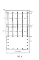
- FIG. 4 is a block diagram illustrating a second exemplary layout design of a circuit board according to the present invention.
- the exemplary circuit board 400 has a layout design similar to that of the exemplary circuit board 100 shown in FIG. 1 . The major difference between them is that the second connector placement site 106_1 dedicated to the second signal processing circuit 214 is closer to the integrated circuit placement site 102 than the first connector placement site 104_1 dedicated to the first signal processing circuit 212.
- FIG. 5 is a block diagram illustrating a first exemplary electronic device employing the circuit board 400 shown in FIG. 4 according to the present invention.
- FIG. 6 is a block diagram illustrating a second exemplary electronic device employing the circuit board 400 shown in FIG. 4 according to the present invention.
- the interface multiplexer 216 of the exemplary electronic device 500 would be controlled to have its output port electrically connected to the second port P2, and the connector 204 is installed on the second connector placement site 106_1 dedicated to the second processing circuit 214.
- the interface multiplexer 216 of the exemplary electronic device 600 would be controlled to have its output port electrically connected to the first port P1, and the connector 304 is installed on the first connector placement site 104_1 dedicated to the first signal processing circuit 212.
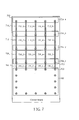
- FIG. 7 is a block diagram illustrating a third exemplary layout design of a circuit board according to the present invention.
- the circuit board 700 has an integrated circuit placement site 702, a plurality of connector placement sites 704_1-704_4, and a plurality of signal traces including first signal traces 706_1-706_5 electrically connected between the integrated circuit placement site 702 and the connector placement site 704_1, second signal traces 708_1-708_5 electrically connected between connector placement sites 704_1 and 704_2, third signal traces 710_1-710 5 electrically connected between connector placement sites 704_2 and 704_3, and fourth signal traces 712_1-712_5 electrically connected between connector placement sites 704 3 and 704_4.
- the integrated circuit placement site 702 has a plurality of connection nodes 703, such as pads or plated through holes (vias).
- each of the connector placement sites 704_1-704_4 has a plurality of connection nodes 705, such as plated through holes (vias).
- the integrated circuit placement site 702 and the connector placement sites 704_1-704_4 are electrically connected in series through the first signal traces 706_1-706_5, the second signal traces 708_1-708_5, the third signal traces 710_1-710_5, and the fourth signal traces 712_1-712_5.
- the connector placement sites 704_1-704_4 include more than one connector placement site dedicated to at least one of the first signal processing circuit 212 and the second signal processing circuit 214.
- the connector placement sites 704_1-704_2 are both dedicated to the first signal processing circuit 212 but correspond to different connector types (i.e., different interface types)
- the connector placement sites 704_3-704_4 are both dedicated to the second signal processing circuit 214 but correspond to different connector types (i.e., different interface types).
- the circuit board 700 supports more connector types for either of the first signal processing circuit 212 and the second signal processing circuit 214, the flexibility in the use of the circuit board 700 can be improved greatly. That is, with a target connector properly installed on one of the connector placement sites 704_1-704_4 defined by the circuit board layout design, a resultant electronic device employing the circuit board 700 to carry the integrated circuit 202 can meet the requirement of a particular application.
- the connector placement sites 704_1-704_2 may be both dedicated to the second signal processing circuit 214 but correspond to different connector types
- the connector placement sites 704_3-704_4 may be both dedicated to the first signal processing circuit 212 but correspond to different connector types. The similar objective of supporting more connector types for either of the first signal processing circuit 212 and the second signal processing circuit 214 is achieved.
- one of the connector placement sites 704_1-704_4 is dedicated to one of the first signal processing circuit 212 and the second signal processing circuit 214, and the remaining connector placement sites are all dedicated to the other of the first signal processing circuit 212 and the second signal processing circuit 214 but correspond to different connector types.
- the similar objective of supporting more connector types for one of the first signal processing circuit 212 and the second signal processing circuit 214 is achieved.
- the connector 304 is installed on the first connector placement site 104_1 closer to the integrated circuit 202 than the second connector placement site 106_1, and the second connector placement site 106_1 has no connector installed thereon.
- the first signal processing circuit 212 is generating an output to an external processing circuit (e.g., an external timing controller) through the connector 304
- the outer second connector placement site 106_1 is electrically connected to the inner first connector placement site 104_1 through the second traces 110_1-110_5.
- the second connector placement site 106_1 which is not used for connector installation but is electrically connected to the first connector placement site 104_1 with the connector 304 installed thereon, may degrade the signal transmission quality of the output of the first signal processing circuit 212.
- the connector 204 is installed on the second connector placement site 106_1 closer to the integrated circuit 202 than the first connector placement site 104_1, and the first connector placement site 104_1 has no connector installed thereon.
- the second signal processing circuit 214 is generating an output to an external apparatus (e.g., an external display panel) through the connector 204
- the outer first connector placement site 104_1 is electrically connected to the inner second connector placement site 106_1 through the second traces 110_1-110_5.
- the first connector placement site 104_1 which is not used for connector installation but is electrically connected to the second connector placement site 106_1 with the connector 204 installed thereon, may degrade the signal transmission quality of the output of the second signal processing circuit 214.
- the present invention therefore proposed an improved circuit board layout design to prevent the undesired signal degradation.
- FIG. 8 is a block diagram illustrating a fourth exemplary layout design of a circuit board according to the present invention.
- the circuit board (e.g., a printed circuit board) 800 has an integrated circuit placement site 802, a plurality of connector placement sites including at least a first connector placement site 804_1 and at least a second connector placement site 806_1, at least a group of passive component placement sites 808_1-808_5 disposed between the first connector placement site 804_1 and the second connector placement site 806_1, and a plurality of signal traces including first signal traces 810_1-810_5, second signal traces 812_1-812_5, and third signal traces 814_1-814_5.
- the integrated circuit placement site 802 has a plurality of connection nodes 803, such as pads or plated through holes (vias).
- the first connector placement site 804_1 has a plurality of connection nodes 805, such as plated through holes (vias);
- the second connector placement site 806_1 has a plurality of connection nodes 807, such as plated through holes (vias);
- each of the passive component placement sites 808_1-808_5 has a plurality of connection nodes 809, such as plated through holes (vias). As shown in FIG.
- the first signal traces 810_1-810_5 are electrically connected between the integrated circuit placement site 802 and the first connector placement site 804_1
- the second signal traces 812_1-812_5 are electrically connected between the first connector placement site 804_1 and the group of passive component placement sites 808_1-808_5
- the third signal traces 814_1-814_5 are electrically connected between the group of passive component placement sites 808_1-808_5 and the second connector placement site 806_1.
- the number of connector placement sites shown in FIG. 8 the number of signal traces shown in FIG. 8
- the number of passive component placement sites shown in FIG. 8 are for illustrative purposes only, and are not meant to be limitations of the present invention.
- the function of the integrated circuit placement site 802 is identical to that of the integrated circuit placement site 102, and the function of the connector placement sites, including the first connector placement site 804_1 and the second connector placement site 806_1, is identical to that of the connector placement sites, including the first connector placement site 104_1 and the second connector placement site 106_1. Further description is omitted here for brevity.
- each of the passive placement sites 808_1-808_5 it is defied to allow a passive component, such as a zero-ohm resistor, to be installed thereon.
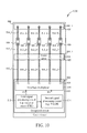
- FIG. 9 is a block diagram illustrating a first exemplary electronic device employing the circuit board 800 shown in FIG. 8 according to the present invention.
- the exemplary electronic device 900 includes, but is not limited to, the integrated circuit 202, the circuit board 800 shown in FIG. 8 , the connector 204 installed on the second connector placement site 806_1, and a plurality of passive components 902_1-902_5 (e.g., zero-ohm resistors) respectively installed on the passive component placement sites 808_1-808_5.
- the first connector placement site 804_1 is dedicated to the first signal processing circuit 212
- the second connector placement site 806_1 is dedicated to the second signal processing circuit 214.
- the interface multiplexer 216 would be controlled to have its output port electrically connected to the second port P2. Therefore, the connector 204 is installed on the second connector placement site 806_1 dedicated to the second processing circuit 214 for allowing the signal transmission between the second signal processing circuit 214 and the external display panel.
- the configuration of the exemplary electronic device 900 shown in FIG. 9 is similar to that of the exemplary electronic device 200 shown in FIG. 2 .
- the second connector placement site 806_1, the first connector placement site 804_1, and the integrated circuit placement site 802 are electrically connected in series through the first signal traces 810_1-810_5, the second signal traces 812_1-812_5, the installed passive components 902_1-902_5, and the third signal traces 814_1-814_5.
- FIG. 10 is a block diagram illustrating a second exemplary electronic device employing the circuit board 800 shown in FIG. 8 according to the present invention.
- the connector 304 is installed on the first connector placement site 804_1 dedicated to the first processing circuit 212.
- each of the passive component placement sites 808_1-808_5 acts as an open circuit.
- the second connector placement site 806_1 would be isolated from the first connector placement site 804_1 on which the connector 304 is installed, thereby avoiding the undesired signal degradation caused by the second connector placement site 806_1.
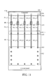
- FIG. 11 is a block diagram illustrating a fifth exemplary layout design of a circuit board according to the present invention.
- the exemplary circuit board 1100 has a layout design similar to that of the exemplary circuit board 800 shown in FIG. 8 . The major difference between them is that the second connector placement site 806_1 is closer to the integrated circuit placement site 802 than the first connector placement site 804_1.
- FIG. 12 is a block diagram illustrating a first exemplary electronic device employing the circuit board 1100 shown in FIG. 11 according to the present invention.
- FIG. 13 is a block diagram illustrating a second exemplary electronic device employing the circuit board shown 1100 in FIG. 11 according to the present invention.
- the interface multiplexer 216 of the exemplary electronic device 1200 would be controlled to have its output port electrically connected to the second port P2, and the connector 204 is installed on the second connector placement site 806_1 dedicated to the second processing circuit 214.
- the interface multiplexer 216 of the exemplary electronic device 1300 would be controlled to have its output port electrically connected to the first port P1, and the connector 304 is installed on the first connector placement site 804_1 dedicated to the first signal processing circuit 212.
- the passive component placement sites 808_1-808_5 have passive components 902_1-902_5 installed thereon, respectively.
- the passive component placement sites 808_1-808_5 have no passive component installed thereon, thereby improving the signal transmission quality.
- the connector type and/or the interference tolerance may be taken into consideration when defining which one of the first connector placement site 804_1 and the second connector placement site 806_1 should be located closer to the integrated circuit placement site 802.
- one of the first connector placement site 804_1 and the second connector placement site 806_1 may be defined for allowing installation of an LVDS connector
- the other of the first connector placement site 804_1 and the second connector placement site 806_1 may be defined for allowing installation of a mini-LVDS connector.
- the connector placement site defined for allowing installation of a mini-LVDS connector would be closer to the integrated circuit placement site 802 than the connector placement site defined for allowing installation of an LVDS connector.
- first connector placement site 804_1 and the second connector placement site 806_1 may be defined for allowing installation of a first connector with a first connector shape
- the other of the first connector placement site 804_1 and the second connector placement site 806_1 may be defined for allowing installation of a second connector with a second connector shape. If installing the first connector on a connector placement site closer to the integrated circuit placement site 802 is easier than installing the first connector on a connector placement site far away from the integrated circuit placement site 802, the connector placement site defined for allowing installation of the first connector with the first connector shape would be closer to the integrated circuit placement site 802 than the connector placement site defined for allowing installation of the second connector with the second connector shape.
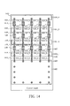
- FIG. 14 is a block diagram illustrating a sixth exemplary layout design of a circuit board according to the present invention.
- the circuit board (e.g., a printed circuit board) 1400 has an integrated circuit placement site 1402, a plurality of connector placement sites 1404_1-1404_4, a plurality of groups of passive component placement sites 1406-1-1406_5, 1408-1-1408_5, and 1410-1-1410_5, and a plurality of signal traces including first signal traces 1412_1-1412_5 electrically connected between the integrated circuit placement site 1402 and the connector placement site 1404_1, second signal traces 1414_1-1414_5 electrically connected between the connector placement site 1404_1 and passive component placement sites 1406_1-1406_5, third signal traces 1416_1-1416_5 electrically connected between the connector placement site 1404_2 and passive component placement sites 1406_1-1406_5, fourth signal traces 1418_1-1418_5 electrically connected between the connector placement site 1404_2 and passive component placement sites 1408_1-1408_5, fifth signal traces 1420_1-1420_5 electrically connected between the connector placement site 1404_3 and passive component
- the integrated circuit placement site 1402 has a plurality of connection nodes 1403, such as pads or plated through holes (vias).
- each of the connector placement sites 1404_1-1404_4 has a plurality of connection nodes 1405, such as plated through holes (vias)
- each of the passive component placement sites 1406_1-1406_5, 1408_1-1408_5, and 1410_1-1410_5 has a plurality of connection nodes 1407, such as plated through holes (vias).
- the connector placement sites 1404_1-1404_4 have more than one connector placement site dedicated to at least one of the first signal processing circuit 212 and the second signal processing circuit 214.
- the connector placement sites 1404_1-1404_2 are both dedicated to the first signal processing circuit 212 but correspond to different connector types (i.e., different interface types)
- the connector placement sites 1404_3-1404_4 are both dedicated to the second signal processing circuit 214 but correspond to different connector types (i.e., different interface types).
- the connector placement sites 1404_1-1404_2 may be both dedicated to the second signal processing circuit 214 but correspond to different connector types
- the connector placement sites 1404_3-1404_4 may be both dedicated to the first signal processing circuit 212 but correspond to different connector types.
- one of the connector placement sites 1404_1-1404_4 is dedicated to one of the first signal processing circuit 212 and the second signal processing circuit 214, and the remaining connector placement sites are all dedicated to the other of the first signal processing circuit 212 and the second signal processing circuit 214 but correspond to different connector types.
- each of the connector placement sites may be configured to have the number of connection nodes equal to a maximum value among the connection pin numbers of all supported connector types. To put it simply, part or all of the connection nodes defined in a connector placement site may be used for actual signal transmission, depending upon a connector type of a connector installed on the connector placement site.
Landscapes
- Engineering & Computer Science (AREA)
- Theoretical Computer Science (AREA)
- Computer Hardware Design (AREA)
- Physics & Mathematics (AREA)
- Microelectronics & Electronic Packaging (AREA)
- Evolutionary Computation (AREA)
- General Engineering & Computer Science (AREA)
- General Physics & Mathematics (AREA)
- Geometry (AREA)
- Architecture (AREA)
- Multimedia (AREA)
- Signal Processing (AREA)
- Combinations Of Printed Boards (AREA)
- Pinball Game Machines (AREA)
- Semiconductor Integrated Circuits (AREA)
- Details Of Connecting Devices For Male And Female Coupling (AREA)
- Printing Elements For Providing Electric Connections Between Printed Circuits (AREA)
Applications Claiming Priority (2)
| Application Number | Priority Date | Filing Date | Title |
|---|---|---|---|
| US36492610P | 2010-07-16 | 2010-07-16 | |
| US13/041,442 US8665606B2 (en) | 2010-07-16 | 2011-03-07 | Electronic device having circuit board with co-layout design of multiple connector placement sites and related circuit board thereof |
Publications (3)
| Publication Number | Publication Date |
|---|---|
| EP2408280A2 true EP2408280A2 (fr) | 2012-01-18 |
| EP2408280A3 EP2408280A3 (fr) | 2012-11-28 |
| EP2408280B1 EP2408280B1 (fr) | 2013-11-20 |
Family
ID=44903498
Family Applications (1)
| Application Number | Title | Priority Date | Filing Date |
|---|---|---|---|
| EP11002112.8A Active EP2408280B1 (fr) | 2010-07-16 | 2011-03-14 | Dispositif électronique doté d'un circuit imprimé avec un design commun de sites de positionnement de connecteur multiple et circuit imprimé correspondant |
Country Status (4)
| Country | Link |
|---|---|
| US (2) | US8665606B2 (fr) |
| EP (1) | EP2408280B1 (fr) |
| CN (2) | CN102340923B (fr) |
| TW (1) | TWI434630B (fr) |
Cited By (1)
| Publication number | Priority date | Publication date | Assignee | Title |
|---|---|---|---|---|
| WO2019137661A1 (fr) * | 2018-01-10 | 2019-07-18 | Huf Hülsbeck & Fürst Gmbh & Co. Kg | Carte de circuit imprimé pour la connexion à une matrice de broches de contact de connecteurs électriques |
Families Citing this family (22)
| Publication number | Priority date | Publication date | Assignee | Title |
|---|---|---|---|---|
| US8665606B2 (en) * | 2010-07-16 | 2014-03-04 | Mediatek Inc. | Electronic device having circuit board with co-layout design of multiple connector placement sites and related circuit board thereof |
| EP2681730B1 (fr) * | 2011-03-02 | 2022-08-17 | Stratacache, Inc. | Porte équipée d'un système d'affichage numérique translucide |
| GB2495607B (en) * | 2011-10-11 | 2014-07-02 | Lg Display Co Ltd | Liquid crystal display device and driving method thereof |
| US9881528B2 (en) | 2011-10-13 | 2018-01-30 | Manufacturing Resources International, Inc. | Transparent liquid crystal display on display case |
| KR101987191B1 (ko) * | 2012-08-31 | 2019-09-30 | 엘지디스플레이 주식회사 | 액정 디스플레이 장치와 이의 구동방법 |
| US8964118B2 (en) * | 2013-04-12 | 2015-02-24 | Shenzhen China Star Optoelectronics Technology Co., Ltd. | Display signal processing system, circuit board, and liquid crystal display |
| US9500896B2 (en) | 2014-06-16 | 2016-11-22 | Manufacturing Resources International, Inc. | Cooling system for liquid crystal display |
| US9535293B2 (en) | 2014-06-16 | 2017-01-03 | Manufacturing Resources International, Inc. | Sealed transparent liquid crystal display assembly |
| US9633366B2 (en) | 2014-06-16 | 2017-04-25 | Manufacturing Resources International, Inc. | System for tracking and analyzing display case usage |
| US10649273B2 (en) | 2014-10-08 | 2020-05-12 | Manufacturing Resources International, Inc. | LED assembly for transparent liquid crystal display and static graphic |
| US9832847B2 (en) | 2014-10-09 | 2017-11-28 | Manufacturing Resources International, Inc. | System for decreasing energy usage of a transparent LCD display case |
| US10182665B2 (en) | 2014-10-15 | 2019-01-22 | Manufacturing Resources International, Inc. | System and method for preventing damage to products |
| CN104331133B (zh) * | 2014-11-07 | 2018-02-06 | 浪潮(北京)电子信息产业有限公司 | 一种硬盘背板和硬盘存储系统 |
| US9763333B2 (en) * | 2015-03-09 | 2017-09-12 | Cooper Technologies Company | Shared resistor pad bypass |
| CN105516753B (zh) * | 2015-12-02 | 2018-09-18 | 深圳市华星光电技术有限公司 | 液晶电视装置及系统 |
| WO2017151934A1 (fr) | 2016-03-02 | 2017-09-08 | Manufacturing Resources International, Inc. | Distributeur automatique doté d'un affichage transparent |
| JP2019527849A (ja) | 2016-07-08 | 2019-10-03 | マニュファクチャリング・リソーシズ・インターナショナル・インコーポレーテッド | 一体型電子ディスプレイを有するミラー |
| CN106535472B (zh) * | 2017-01-12 | 2019-08-02 | 郑州云海信息技术有限公司 | 一种pcb及信号传输系统 |
| US10880514B2 (en) * | 2018-11-27 | 2020-12-29 | Hisense Visual Technology Co., Ltd. | Method and TV set for transmitting image data |
| US11924966B1 (en) * | 2021-07-09 | 2024-03-05 | Innovium, Inc. | Reconfigurable circuit devices |
| TWI868664B (zh) * | 2023-04-13 | 2025-01-01 | 瑞昱半導體股份有限公司 | 印刷電路板的電路布局 |
| CN118829065B (zh) * | 2023-04-21 | 2025-10-21 | 瑞昱半导体股份有限公司 | 印刷电路板的电路布局 |
Family Cites Families (14)
| Publication number | Priority date | Publication date | Assignee | Title |
|---|---|---|---|---|
| US5192999A (en) * | 1991-04-25 | 1993-03-09 | Compuadd Corporation | Multipurpose computerized television |
| JP3332443B2 (ja) * | 1993-01-18 | 2002-10-07 | キヤノン株式会社 | 情報処理装置および情報処理方法 |
| US20030002541A1 (en) * | 2001-06-07 | 2003-01-02 | Fowler Michael L. | Mid-connect architecture with point-to-point connections for high speed data transfer |
| KR100846459B1 (ko) * | 2001-12-26 | 2008-07-16 | 삼성전자주식회사 | 통합형 커넥터를 갖는 액정표시모듈과 이를 구비하는액정표시장치 |
| US7516272B2 (en) * | 2003-03-28 | 2009-04-07 | Emc Corporation | Midplane-independent implementations of data storage system enclosures |
| CN100346388C (zh) * | 2004-06-08 | 2007-10-31 | 友达光电股份有限公司 | 液晶显示器的数字图像信号处理装置 |
| US7362589B2 (en) | 2005-01-18 | 2008-04-22 | Hewlett-Packard Development Company, L.P. | Circuit board adapted to couple to different types of add-in cards |
| US20070038794A1 (en) * | 2005-08-10 | 2007-02-15 | Purcell Brian T | Method and system for allocating a bus |
| CN101038732A (zh) * | 2006-03-16 | 2007-09-19 | 奇景光电股份有限公司 | 整合型图像控制芯片组 |
| CN100561455C (zh) * | 2006-09-01 | 2009-11-18 | 鸿富锦精密工业(深圳)有限公司 | 高速差分信号传输硬件架构 |
| US7941053B2 (en) * | 2006-10-19 | 2011-05-10 | Emcore Corporation | Optical transceiver for 40 gigabit/second transmission |
| CN101636040B (zh) | 2008-07-21 | 2011-12-14 | 鸿富锦精密工业(深圳)有限公司 | 印刷电路板 |
| JPWO2010050555A1 (ja) * | 2008-10-31 | 2012-03-29 | オリンパスメディカルシステムズ株式会社 | 超音波観測装置 |
| US8665606B2 (en) * | 2010-07-16 | 2014-03-04 | Mediatek Inc. | Electronic device having circuit board with co-layout design of multiple connector placement sites and related circuit board thereof |
-
2011
- 2011-03-07 US US13/041,442 patent/US8665606B2/en active Active
- 2011-03-14 EP EP11002112.8A patent/EP2408280B1/fr active Active
- 2011-07-11 TW TW100124463A patent/TWI434630B/zh not_active IP Right Cessation
- 2011-07-12 CN CN201110193822.2A patent/CN102340923B/zh active Active
- 2011-07-12 CN CN201510090308.4A patent/CN104640346B/zh active Active
-
2014
- 2014-01-20 US US14/158,876 patent/US9183340B2/en active Active
Non-Patent Citations (1)
| Title |
|---|
| None |
Cited By (2)
| Publication number | Priority date | Publication date | Assignee | Title |
|---|---|---|---|---|
| WO2019137661A1 (fr) * | 2018-01-10 | 2019-07-18 | Huf Hülsbeck & Fürst Gmbh & Co. Kg | Carte de circuit imprimé pour la connexion à une matrice de broches de contact de connecteurs électriques |
| JP2021510236A (ja) * | 2018-01-10 | 2021-04-15 | フーフ・ヒュルスベック・ウント・フュルスト・ゲーエムベーハー・ウント・コンパニー・カーゲーHuf Hulsbeck & Furst Gmbh & Co. Kg | 電気コネクタの接点ピンのマトリクスと接続するための導体路基板 |
Also Published As
| Publication number | Publication date |
|---|---|
| US20140137065A1 (en) | 2014-05-15 |
| CN104640346B (zh) | 2018-02-09 |
| CN104640346A (zh) | 2015-05-20 |
| TW201212748A (en) | 2012-03-16 |
| TWI434630B (zh) | 2014-04-11 |
| US8665606B2 (en) | 2014-03-04 |
| US9183340B2 (en) | 2015-11-10 |
| CN102340923B (zh) | 2015-04-01 |
| US20120014080A1 (en) | 2012-01-19 |
| EP2408280B1 (fr) | 2013-11-20 |
| CN102340923A (zh) | 2012-02-01 |
| EP2408280A3 (fr) | 2012-11-28 |
Similar Documents
| Publication | Publication Date | Title |
|---|---|---|
| EP2408280A2 (fr) | Dispositif électronique doté d'un circuit imprimé avec un design commun de sites de positionnement de connecteur multiple et circuit imprimé correspondant | |
| US7246190B2 (en) | Method and apparatus for bringing bus lanes in a computer system using a jumper board | |
| US7596649B2 (en) | Motherboard | |
| JP2008514017A (ja) | 高速相互接続用可撓性ケーブル | |
| KR102803207B1 (ko) | 디스플레이 장치, 구동 회로 및 구동 방법 | |
| JP4997593B2 (ja) | 表示装置 | |
| CN207038050U (zh) | 阵列基板及显示装置 | |
| US20150085452A1 (en) | Layout method, electronic device and connector | |
| KR100801174B1 (ko) | 표시장치 및 타이밍 컨트롤러 | |
| CN110888498B (zh) | 计算装置及快速周边组件互连基板 | |
| EP3462485A1 (fr) | Dispositifs semiconducteurs et procédés permettant d'améliorer l'intégrité du signal d'une interface fournie par un dispositif à semiconducteur | |
| JP2002287655A (ja) | 表示装置 | |
| EP2472313A1 (fr) | Dispositif d'affichage à cristaux liquides du type à puce sur verre | |
| CN202771345U (zh) | Pxi背板和便携式pxi机箱 | |
| CN101192394B (zh) | 半导体装置及使用了它的电子设备 | |
| US7764509B2 (en) | Method and apparatus for interfacing components | |
| CN201854499U (zh) | 印刷电路板 | |
| JP2011164826A (ja) | ユニット収容装置、ユニット、システム、ユニット収容装置の製造方法及びユニット制御方法。 | |
| JPH11212672A (ja) | 情報処理装置、液晶表示装置、集積回路及び配線基板並びに情報処理装置の製造方法 | |
| CN116047882B (zh) | 印刷电路板、覆晶薄膜内充电时间的补偿方法 | |
| EP3200569A1 (fr) | Circuit intégré, dispositif électronique et procédé de transmission de données dans un dispositif électronique | |
| TWI363968B (en) | High speed differential signal transmitting structure | |
| KR20100070788A (ko) | 액정표시장치 | |
| Krause | Design and Implementation of a MIPI CSI-2 compatible receiver and pre-processor for low-resolution image processing | |
| CN102938831B (zh) | 电子装置的控制电路以及显示装置 |
Legal Events
| Date | Code | Title | Description |
|---|---|---|---|
| AK | Designated contracting states |
Kind code of ref document: A2 Designated state(s): AL AT BE BG CH CY CZ DE DK EE ES FI FR GB GR HR HU IE IS IT LI LT LU LV MC MK MT NL NO PL PT RO RS SE SI SK SM TR |
|
| AX | Request for extension of the european patent |
Extension state: BA ME |
|
| PUAI | Public reference made under article 153(3) epc to a published international application that has entered the european phase |
Free format text: ORIGINAL CODE: 0009012 |
|
| REG | Reference to a national code |
Ref country code: DE Ref legal event code: R079 Ref document number: 602011003784 Country of ref document: DE Free format text: PREVIOUS MAIN CLASS: H05K0001110000 Ipc: H05K0001020000 |
|
| PUAL | Search report despatched |
Free format text: ORIGINAL CODE: 0009013 |
|
| AK | Designated contracting states |
Kind code of ref document: A3 Designated state(s): AL AT BE BG CH CY CZ DE DK EE ES FI FR GB GR HR HU IE IS IT LI LT LU LV MC MK MT NL NO PL PT RO RS SE SI SK SM TR |
|
| AX | Request for extension of the european patent |
Extension state: BA ME |
|
| RIC1 | Information provided on ipc code assigned before grant |
Ipc: H05K 1/02 20060101AFI20121019BHEP |
|
| 17P | Request for examination filed |
Effective date: 20130131 |
|
| GRAP | Despatch of communication of intention to grant a patent |
Free format text: ORIGINAL CODE: EPIDOSNIGR1 |
|
| INTG | Intention to grant announced |
Effective date: 20130709 |
|
| RIN1 | Information on inventor provided before grant (corrected) |
Inventor name: WU, HUA Inventor name: LIN, SHANG-YI Inventor name: FENG, HUAI-YUAN Inventor name: LUO, YAN-BIN Inventor name: PAN, CHING-GU |
|
| RIN1 | Information on inventor provided before grant (corrected) |
Inventor name: PAN, CHING-GU Inventor name: LUO, YAN-BIN Inventor name: LIN, SHANG-YI Inventor name: FENG, HUAI-YUAN Inventor name: WU, HUA |
|
| GRAS | Grant fee paid |
Free format text: ORIGINAL CODE: EPIDOSNIGR3 |
|
| GRAA | (expected) grant |
Free format text: ORIGINAL CODE: 0009210 |
|
| AK | Designated contracting states |
Kind code of ref document: B1 Designated state(s): AL AT BE BG CH CY CZ DE DK EE ES FI FR GB GR HR HU IE IS IT LI LT LU LV MC MK MT NL NO PL PT RO RS SE SI SK SM TR |
|
| REG | Reference to a national code |
Ref country code: GB Ref legal event code: FG4D |
|
| REG | Reference to a national code |
Ref country code: CH Ref legal event code: EP |
|
| REG | Reference to a national code |
Ref country code: AT Ref legal event code: REF Ref document number: 642291 Country of ref document: AT Kind code of ref document: T Effective date: 20131215 |
|
| REG | Reference to a national code |
Ref country code: IE Ref legal event code: FG4D |
|
| REG | Reference to a national code |
Ref country code: DE Ref legal event code: R096 Ref document number: 602011003784 Country of ref document: DE Effective date: 20140116 |
|
| REG | Reference to a national code |
Ref country code: NL Ref legal event code: VDEP Effective date: 20131120 |
|
| REG | Reference to a national code |
Ref country code: AT Ref legal event code: MK05 Ref document number: 642291 Country of ref document: AT Kind code of ref document: T Effective date: 20131120 |
|
| REG | Reference to a national code |
Ref country code: LT Ref legal event code: MG4D |
|
| PG25 | Lapsed in a contracting state [announced via postgrant information from national office to epo] |
Ref country code: HR Free format text: LAPSE BECAUSE OF FAILURE TO SUBMIT A TRANSLATION OF THE DESCRIPTION OR TO PAY THE FEE WITHIN THE PRESCRIBED TIME-LIMIT Effective date: 20131120 Ref country code: SE Free format text: LAPSE BECAUSE OF FAILURE TO SUBMIT A TRANSLATION OF THE DESCRIPTION OR TO PAY THE FEE WITHIN THE PRESCRIBED TIME-LIMIT Effective date: 20131120 Ref country code: NO Free format text: LAPSE BECAUSE OF FAILURE TO SUBMIT A TRANSLATION OF THE DESCRIPTION OR TO PAY THE FEE WITHIN THE PRESCRIBED TIME-LIMIT Effective date: 20140220 Ref country code: LT Free format text: LAPSE BECAUSE OF FAILURE TO SUBMIT A TRANSLATION OF THE DESCRIPTION OR TO PAY THE FEE WITHIN THE PRESCRIBED TIME-LIMIT Effective date: 20131120 Ref country code: NL Free format text: LAPSE BECAUSE OF FAILURE TO SUBMIT A TRANSLATION OF THE DESCRIPTION OR TO PAY THE FEE WITHIN THE PRESCRIBED TIME-LIMIT Effective date: 20131120 Ref country code: FI Free format text: LAPSE BECAUSE OF FAILURE TO SUBMIT A TRANSLATION OF THE DESCRIPTION OR TO PAY THE FEE WITHIN THE PRESCRIBED TIME-LIMIT Effective date: 20131120 Ref country code: IS Free format text: LAPSE BECAUSE OF FAILURE TO SUBMIT A TRANSLATION OF THE DESCRIPTION OR TO PAY THE FEE WITHIN THE PRESCRIBED TIME-LIMIT Effective date: 20140320 |
|
| PG25 | Lapsed in a contracting state [announced via postgrant information from national office to epo] |
Ref country code: AT Free format text: LAPSE BECAUSE OF FAILURE TO SUBMIT A TRANSLATION OF THE DESCRIPTION OR TO PAY THE FEE WITHIN THE PRESCRIBED TIME-LIMIT Effective date: 20131120 Ref country code: BE Free format text: LAPSE BECAUSE OF FAILURE TO SUBMIT A TRANSLATION OF THE DESCRIPTION OR TO PAY THE FEE WITHIN THE PRESCRIBED TIME-LIMIT Effective date: 20131120 Ref country code: ES Free format text: LAPSE BECAUSE OF FAILURE TO SUBMIT A TRANSLATION OF THE DESCRIPTION OR TO PAY THE FEE WITHIN THE PRESCRIBED TIME-LIMIT Effective date: 20131120 Ref country code: RS Free format text: LAPSE BECAUSE OF FAILURE TO SUBMIT A TRANSLATION OF THE DESCRIPTION OR TO PAY THE FEE WITHIN THE PRESCRIBED TIME-LIMIT Effective date: 20131120 Ref country code: LV Free format text: LAPSE BECAUSE OF FAILURE TO SUBMIT A TRANSLATION OF THE DESCRIPTION OR TO PAY THE FEE WITHIN THE PRESCRIBED TIME-LIMIT Effective date: 20131120 |
|
| PG25 | Lapsed in a contracting state [announced via postgrant information from national office to epo] |
Ref country code: PT Free format text: LAPSE BECAUSE OF FAILURE TO SUBMIT A TRANSLATION OF THE DESCRIPTION OR TO PAY THE FEE WITHIN THE PRESCRIBED TIME-LIMIT Effective date: 20140320 |
|
| PG25 | Lapsed in a contracting state [announced via postgrant information from national office to epo] |
Ref country code: EE Free format text: LAPSE BECAUSE OF FAILURE TO SUBMIT A TRANSLATION OF THE DESCRIPTION OR TO PAY THE FEE WITHIN THE PRESCRIBED TIME-LIMIT Effective date: 20131120 |
|
| REG | Reference to a national code |
Ref country code: DE Ref legal event code: R097 Ref document number: 602011003784 Country of ref document: DE |
|
| PG25 | Lapsed in a contracting state [announced via postgrant information from national office to epo] |
Ref country code: CZ Free format text: LAPSE BECAUSE OF FAILURE TO SUBMIT A TRANSLATION OF THE DESCRIPTION OR TO PAY THE FEE WITHIN THE PRESCRIBED TIME-LIMIT Effective date: 20131120 Ref country code: RO Free format text: LAPSE BECAUSE OF FAILURE TO SUBMIT A TRANSLATION OF THE DESCRIPTION OR TO PAY THE FEE WITHIN THE PRESCRIBED TIME-LIMIT Effective date: 20131120 Ref country code: SK Free format text: LAPSE BECAUSE OF FAILURE TO SUBMIT A TRANSLATION OF THE DESCRIPTION OR TO PAY THE FEE WITHIN THE PRESCRIBED TIME-LIMIT Effective date: 20131120 Ref country code: PL Free format text: LAPSE BECAUSE OF FAILURE TO SUBMIT A TRANSLATION OF THE DESCRIPTION OR TO PAY THE FEE WITHIN THE PRESCRIBED TIME-LIMIT Effective date: 20131120 |
|
| PLBE | No opposition filed within time limit |
Free format text: ORIGINAL CODE: 0009261 |
|
| STAA | Information on the status of an ep patent application or granted ep patent |
Free format text: STATUS: NO OPPOSITION FILED WITHIN TIME LIMIT |
|
| PG25 | Lapsed in a contracting state [announced via postgrant information from national office to epo] |
Ref country code: DK Free format text: LAPSE BECAUSE OF FAILURE TO SUBMIT A TRANSLATION OF THE DESCRIPTION OR TO PAY THE FEE WITHIN THE PRESCRIBED TIME-LIMIT Effective date: 20131120 |
|
| 26N | No opposition filed |
Effective date: 20140821 |
|
| PG25 | Lapsed in a contracting state [announced via postgrant information from national office to epo] |
Ref country code: LU Free format text: LAPSE BECAUSE OF FAILURE TO SUBMIT A TRANSLATION OF THE DESCRIPTION OR TO PAY THE FEE WITHIN THE PRESCRIBED TIME-LIMIT Effective date: 20140314 |
|
| REG | Reference to a national code |
Ref country code: CH Ref legal event code: PL |
|
| REG | Reference to a national code |
Ref country code: DE Ref legal event code: R097 Ref document number: 602011003784 Country of ref document: DE Effective date: 20140821 |
|
| REG | Reference to a national code |
Ref country code: IE Ref legal event code: MM4A |
|
| PG25 | Lapsed in a contracting state [announced via postgrant information from national office to epo] |
Ref country code: LI Free format text: LAPSE BECAUSE OF NON-PAYMENT OF DUE FEES Effective date: 20140331 Ref country code: IE Free format text: LAPSE BECAUSE OF NON-PAYMENT OF DUE FEES Effective date: 20140314 Ref country code: CH Free format text: LAPSE BECAUSE OF NON-PAYMENT OF DUE FEES Effective date: 20140331 |
|
| PG25 | Lapsed in a contracting state [announced via postgrant information from national office to epo] |
Ref country code: SI Free format text: LAPSE BECAUSE OF FAILURE TO SUBMIT A TRANSLATION OF THE DESCRIPTION OR TO PAY THE FEE WITHIN THE PRESCRIBED TIME-LIMIT Effective date: 20131120 |
|
| PG25 | Lapsed in a contracting state [announced via postgrant information from national office to epo] |
Ref country code: IT Free format text: LAPSE BECAUSE OF FAILURE TO SUBMIT A TRANSLATION OF THE DESCRIPTION OR TO PAY THE FEE WITHIN THE PRESCRIBED TIME-LIMIT Effective date: 20131120 |
|
| PG25 | Lapsed in a contracting state [announced via postgrant information from national office to epo] |
Ref country code: MT Free format text: LAPSE BECAUSE OF FAILURE TO SUBMIT A TRANSLATION OF THE DESCRIPTION OR TO PAY THE FEE WITHIN THE PRESCRIBED TIME-LIMIT Effective date: 20131120 |
|
| REG | Reference to a national code |
Ref country code: FR Ref legal event code: PLFP Year of fee payment: 6 |
|
| PG25 | Lapsed in a contracting state [announced via postgrant information from national office to epo] |
Ref country code: SM Free format text: LAPSE BECAUSE OF FAILURE TO SUBMIT A TRANSLATION OF THE DESCRIPTION OR TO PAY THE FEE WITHIN THE PRESCRIBED TIME-LIMIT Effective date: 20131120 |
|
| PG25 | Lapsed in a contracting state [announced via postgrant information from national office to epo] |
Ref country code: MC Free format text: LAPSE BECAUSE OF FAILURE TO SUBMIT A TRANSLATION OF THE DESCRIPTION OR TO PAY THE FEE WITHIN THE PRESCRIBED TIME-LIMIT Effective date: 20131120 |
|
| PG25 | Lapsed in a contracting state [announced via postgrant information from national office to epo] |
Ref country code: GR Free format text: LAPSE BECAUSE OF FAILURE TO SUBMIT A TRANSLATION OF THE DESCRIPTION OR TO PAY THE FEE WITHIN THE PRESCRIBED TIME-LIMIT Effective date: 20140221 Ref country code: BG Free format text: LAPSE BECAUSE OF FAILURE TO SUBMIT A TRANSLATION OF THE DESCRIPTION OR TO PAY THE FEE WITHIN THE PRESCRIBED TIME-LIMIT Effective date: 20131120 Ref country code: CY Free format text: LAPSE BECAUSE OF FAILURE TO SUBMIT A TRANSLATION OF THE DESCRIPTION OR TO PAY THE FEE WITHIN THE PRESCRIBED TIME-LIMIT Effective date: 20131120 |
|
| PG25 | Lapsed in a contracting state [announced via postgrant information from national office to epo] |
Ref country code: HU Free format text: LAPSE BECAUSE OF FAILURE TO SUBMIT A TRANSLATION OF THE DESCRIPTION OR TO PAY THE FEE WITHIN THE PRESCRIBED TIME-LIMIT; INVALID AB INITIO Effective date: 20110314 Ref country code: TR Free format text: LAPSE BECAUSE OF FAILURE TO SUBMIT A TRANSLATION OF THE DESCRIPTION OR TO PAY THE FEE WITHIN THE PRESCRIBED TIME-LIMIT Effective date: 20131120 |
|
| REG | Reference to a national code |
Ref country code: FR Ref legal event code: PLFP Year of fee payment: 7 |
|
| REG | Reference to a national code |
Ref country code: FR Ref legal event code: PLFP Year of fee payment: 8 |
|
| PG25 | Lapsed in a contracting state [announced via postgrant information from national office to epo] |
Ref country code: MK Free format text: LAPSE BECAUSE OF FAILURE TO SUBMIT A TRANSLATION OF THE DESCRIPTION OR TO PAY THE FEE WITHIN THE PRESCRIBED TIME-LIMIT Effective date: 20131120 |
|
| PG25 | Lapsed in a contracting state [announced via postgrant information from national office to epo] |
Ref country code: AL Free format text: LAPSE BECAUSE OF FAILURE TO SUBMIT A TRANSLATION OF THE DESCRIPTION OR TO PAY THE FEE WITHIN THE PRESCRIBED TIME-LIMIT Effective date: 20131120 |
|
| P01 | Opt-out of the competence of the unified patent court (upc) registered |
Effective date: 20230607 |
|
| PGFP | Annual fee paid to national office [announced via postgrant information from national office to epo] |
Ref country code: FR Payment date: 20251231 Year of fee payment: 16 |
|
| PGFP | Annual fee paid to national office [announced via postgrant information from national office to epo] |
Ref country code: GB Payment date: 20260106 Year of fee payment: 16 |
|
| PGFP | Annual fee paid to national office [announced via postgrant information from national office to epo] |
Ref country code: DE Payment date: 20260102 Year of fee payment: 16 |