EP2410362A2 - Optische Rückwandleiterplatte - Google Patents
Optische Rückwandleiterplatte Download PDFInfo
- Publication number
- EP2410362A2 EP2410362A2 EP11005306A EP11005306A EP2410362A2 EP 2410362 A2 EP2410362 A2 EP 2410362A2 EP 11005306 A EP11005306 A EP 11005306A EP 11005306 A EP11005306 A EP 11005306A EP 2410362 A2 EP2410362 A2 EP 2410362A2
- Authority
- EP
- European Patent Office
- Prior art keywords
- interconnections
- component
- optical
- backplane
- components
- Prior art date
- Legal status (The legal status is an assumption and is not a legal conclusion. Google has not performed a legal analysis and makes no representation as to the accuracy of the status listed.)
- Withdrawn
Links
- 230000003287 optical effect Effects 0.000 title claims abstract description 80
- 238000000034 method Methods 0.000 claims description 20
- 239000000835 fiber Substances 0.000 claims description 18
- 238000005516 engineering process Methods 0.000 claims description 16
- 229920000642 polymer Polymers 0.000 claims description 5
- 230000003068 static effect Effects 0.000 claims description 4
- RYGMFSIKBFXOCR-UHFFFAOYSA-N Copper Chemical compound [Cu] RYGMFSIKBFXOCR-UHFFFAOYSA-N 0.000 description 14
- 229910052802 copper Inorganic materials 0.000 description 14
- 239000010949 copper Substances 0.000 description 14
- 238000010586 diagram Methods 0.000 description 4
- 238000004590 computer program Methods 0.000 description 3
- 238000013461 design Methods 0.000 description 3
- 238000005265 energy consumption Methods 0.000 description 3
- 239000010410 layer Substances 0.000 description 3
- 208000032365 Electromagnetic interference Diseases 0.000 description 2
- 238000004891 communication Methods 0.000 description 2
- 238000012545 processing Methods 0.000 description 2
- 238000012423 maintenance Methods 0.000 description 1
- 239000002861 polymer material Substances 0.000 description 1
- 239000002356 single layer Substances 0.000 description 1
Images


Classifications
-
- G—PHYSICS
- G02—OPTICS
- G02B—OPTICAL ELEMENTS, SYSTEMS OR APPARATUS
- G02B6/00—Light guides; Structural details of arrangements comprising light guides and other optical elements, e.g. couplings
- G02B6/24—Coupling light guides
- G02B6/36—Mechanical coupling means
- G02B6/38—Mechanical coupling means having fibre to fibre mating means
- G02B6/3807—Dismountable connectors, i.e. comprising plugs
- G02B6/3897—Connectors fixed to housings, casing, frames or circuit boards
-
- G—PHYSICS
- G02—OPTICS
- G02B—OPTICAL ELEMENTS, SYSTEMS OR APPARATUS
- G02B6/00—Light guides; Structural details of arrangements comprising light guides and other optical elements, e.g. couplings
- G02B6/24—Coupling light guides
- G02B6/42—Coupling light guides with opto-electronic elements
- G02B6/43—Arrangements comprising a plurality of opto-electronic elements and associated optical interconnections
-
- H—ELECTRICITY
- H04—ELECTRIC COMMUNICATION TECHNIQUE
- H04B—TRANSMISSION
- H04B10/00—Transmission systems employing electromagnetic waves other than radio-waves, e.g. infrared, visible or ultraviolet light, or employing corpuscular radiation, e.g. quantum communication
- H04B10/80—Optical aspects relating to the use of optical transmission for specific applications, not provided for in groups H04B10/03 - H04B10/70, e.g. optical power feeding or optical transmission through water
- H04B10/801—Optical aspects relating to the use of optical transmission for specific applications, not provided for in groups H04B10/03 - H04B10/70, e.g. optical power feeding or optical transmission through water using optical interconnects, e.g. light coupled isolators, circuit board interconnections
Definitions
- the present invention relates to telecommunication systems and more specifically to backplanes used for building such systems.
- PCBs Printed Circuit Boards
- blades or nodes
- the chassis 5 allows designing scalable systems i.e. systems into which additional components can be added.
- each component is connected to a backplane 10, also illustrated in figure 1 .
- a backplane is typically a PCB having slots into which other components such as PCBs, blades or cards, are plugged, and is typically just a connector without active surface mounted devices on it.
- the function of the backplane 10 is to carry the communication signals between the components.
- a backplane is passive i.e. it does not require any external electrical power and it is built in such a way that copper traces can be used to exchange information between the components.
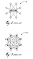
- the backplane is designed to support a network topology such as a star, a dual-star 50 as illustrated in figure 2 , a dual-dual-star or a fully-connected 75 network topology, as illustrated in figure 3 .
- a network topology such as a star, a dual-star 50 as illustrated in figure 2
- a dual-dual-star or a fully-connected 75 network topology as illustrated in figure 3 .
- more or less copper traces might be required, as shown in the figures 2 and 3 , where each circle represents a component and the lines in between the circles represent the interconnections between the components.
- copper traces are sensitive to interferences and offer a limited bandwidth capacity, which means that several parallel traces might be required to fulfill a given bandwidth requirement.
- copper-based backplanes are passive, they provide a network topology adapted for use with a fixed or slightly variable number of components connected to it.
- an optical backplane comprising a plurality of component connectors and at least two interconnections configurations interconnecting the component connectors.
- the at least two interconnections configurations allowing a selection of an interconnections configuration interconnecting the component connectors.
- a method for sending an optical signal from a sending component to a receiving component is also provided.
- the components are connected to an optical backplane through component connectors.
- the method comprises the steps of selecting one of at least two interconnections configurations interconnecting the component connectors of the optical backplane and sending the optical signal to the receiving component through the selected interconnections configuration.
- a method for receiving an optical signal at a receiving component from a sending component is further provided.
- the components are connected to an optical backplane through component connectors.
- the method comprises the steps of selecting one of at least two interconnections configurations interconnecting the component connectors of the optical backplane on which an optical signal is being transmitted at a given time and receiving the optical signal from the sending component through the selected interconnections configuration.
- each block of the block diagrams and/or operational illustrations, and combinations of blocks in the block diagrams and/or operational illustrations can be implemented by radio frequency, analog and/or digital hardware, and/or computer program instructions.
- These computer program instructions may be provided to a processor circuit of a general purpose computer, special purpose computer, ASIC, and/or other programmable data processing apparatus, such that the instructions, which execute via the processor of the computer and/or other programmable data processing apparatus, create means for implementing the functions/acts specified in the block diagrams and/or operational block or blocks.
- the functions/acts noted in the blocks may occur out of the order noted in the operational illustrations.
- two blocks shown in succession may in fact be executed substantially concurrently or the blocks may sometimes be executed in the reverse order, depending upon the functionality/acts involved.
- Fiber optics is already used to interconnect systems requiring a large network bandwidth and covering long distances. Fiber optics consumes far less energy than copper traces. As fiber optics technology develops and becomes more affordable and as internal systems process more and more data, fiber optics technology is now becoming a viable solution for replacing traditional copper traces in a variety of systems.
- This invention takes advantage of the fiber optics technology, in order to simplify the design of backplanes, where optical interconnections replace traditional copper traces, offering a much higher bandwidth per trace. Additionally, optical interconnections are not sensitive to electro-magnetic interference and do not consume as much energy.
- PCBs Printed Circuit Boards
- blades or nodes interconnected through the same backplane
- a multiple layered backplane could more easily account for a multiplicity of traces to interconnect components in multiple configurations.
- optical-based technologies Taking advantage of the large bandwidth allowed by optical-based technologies, it is expected that the number of optical traces required on a backplane to fulfill the requirements of certain network topologies would be far less than for copper-based technologies. Also, as electro-magnetic interference is not an issue for optical signals, the design complexity of an optical backplane is mainly proportional to the number of optical links.
- the polymer waveguide technology which can be used to integrate optical signals in backplanes, making the building of a backplane similar to the process used for the traditional copper-based backplanes.
- Those skilled in the art will know how to use this technology for building optical traces on components.
- the technology to building optical backplanes e.g. the polymer waveguide technology is already available and can be used to build optical backplanes.
- backplanes are designed with one interconnection configuration and if another configuration is needed, another backplane has to be used. Therefore, there is a need for a way to reconfigure the backplane based on the number of components connected to the backplane or based on bandwidth capacity requirement depending on a type of components or an interconnection topology.
- Figure 4 illustrates an optical backplane 15, comprising a plurality of component connectors 110 and at least two interconnections configurations 100 interconnecting the component connectors 110.
- the at least two interconnections configurations 100 allow a selection of an interconnections configuration 100 interconnecting the component connectors 110.
- each one of the at least two interconnections configurations 100 interconnecting the component connectors 110 are optical, passive and static.
- the selection of an interconnections configuration 100 interconnecting the component connectors 110 is preferably based on a number of components 120 connected to the component connectors or is based on bandwidth capacity requirement depending on a type of components or on an interconnection topology.
- Another possibility for selecting the right interconnections configuration could also be based on the type of components 120, which could potentially be requiring more or less bandwidth capacity based on the type of components 120, or based on the interconnection topology.
- the interconnections configurations 100 are preferably network topology interconnections configurations.
- network topology interconnections configurations For example, in the case where the backplane would be built to support a fully-connected network topology, there could be several network configurations for a scalable number of components in the chassis. In other words, depending on the number of network components such as PCBs, blades or nodes, connected to the backplane, one particular network topology configuration would be used.
- the configuration N on the backplane 15 could be used, for example, by each component 120, in order to properly interconnect the components 120 as expected for optimal performance.
- the configuration 2 could be used instead, for example, the other interconnections configurations 100 remaining unused.
- the number of interconnections configurations does not have to be the same as the number of components 120. It should be clear that even for a N-component system, M interconnections configurations could be possible, with M greater then zero.
- the optical backplane is built using a polymer waveguide technology.
- the component connectors 110 each comprise a plurality of links, each link being connected to a different interconnections configuration 100.
- the component connectors 110 may thus each comprise a single ribbon-fiber cable containing multiple fiber waveguides where each link corresponds to one fiber waveguide, for example. It should be understood that each link described above could contain a plurality of physical links, if needed, and that the actual number of physical links should be dictated by the capacity of such unitary physical link and by the bandwidth requirements for each components 120.
- each component 120, or network node can be connected to the backplane 15 using a certain number of links in a component connector 110. If we assume that each link is connected to a different backplane interconnections configuration 100, it becomes possible for each component to select which configuration it needs to use for exchanging information with the other components. For example, as components are added or removed to/from the system, each component could select a different backplane interconnections configuration 100.
- a particular backplane configuration could imply direct inteconnection between the components 120 involved in the configuration, and/or some form of point to multipoint configuration.
- the interconnections configuration 100 may comprise an optical crossbar on the backplane 15 to redirect optical waveguides between the component connectors 110.
- the optical crossbar on the backplane would be specified in order to redirect the different optical waveguides efficiently between the components, as it would be apparent to a person skilled in the art.
- the component connectors may be component slots or other means for connecting for instance a blade or Printed Circuit Board (PCB) to a backplane.
- the components 120 may be PCBs or other components that may be connected to a backplane.
- the optical backplane may comprise a single layer holding one or several interconnections configurations.
- the optical backplane 15 may also comprise at least two layers where, for example a first and a second interconnections configuration 100 are located respectively in a first and a second layer of the optical backplane 15. This has the advantage of increasing the number of configuration possible on the backplane 15. Interconnections configurations 100 spreading on multiple layers of the multi-layer backplane 15 are also considered as being part of the invention.
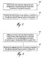
- Figure 5 illustrates steps of a method for sending an optical signal from a sending component to a receiving component.
- the components are connected to an optical backplane through component connectors and the method comprises the step 200 of selecting one of at least two interconnections configurations interconnecting the component connectors of the optical backplane and the step 202 of sending the optical signal to the receiving component through the selected interconnections configuration.
- the step of selecting one of at least two interconnections configurations may be based on a number of components connected to the component connectors or may be based on bandwidth capacity requirement depending on a type of components or on an interconnection topology.
- the sending component may then be responsible for selecting the right interconnections configurations, while the receiving component simply listens on all the interconnections configurations to receive the optical signals, trusting the sending component to select only one such interconnections configuration.
- Figure 6 illustrates steps of a method for receiving an optical signal at a receiving component from a sending component.
- the components are connected to an optical backplane through component connectors and the method comprises the step 210 of selecting one of at least two interconnections configurations interconnecting the component connectors of the optical backplane on which an optical signal is being transmitted at a given time and the step 212 of receiving the optical signal from the sending component through the selected interconnections configuration.
- the step of selecting one of at least two interconnections configurations may be based on a number of components connected to the component connectors or may be based on bandwidth capacity requirement depending on a type of components or on an interconnection topology.
- the sending component thus sends the optical signals through all the different interconnections configurations, and the receiving component accepts optical signals from only one of the interconnections configurations. Basically, even though the optical signals go through all the interconnections configurations, the optical signals should be considered valid on only one of the interconnections configuration.
- the sending component or sender may be responsible for selecting the backplane configuration, in which case the receiving component or receiver simply receives light from all the interconnections configurations 100, assuming that only one interconnections configuration at a time is being used.
- the receiving components could be left to the receiving components to filter out the information, in which case the sending components would send light to all configurations, and the receiving components would have to select the right configuration.
- the solution where the selection is made on the receiving side is possible, but not really efficient, as it requires more powerful optical signals in order for the light to go through all the different backplane interconnections configurations 100.
- each component may be connected to the backplane using a single ribbon-fiber cable.
- a ribbon-fiber cable is a cable that contains multiple fiber waveguides.
- the ribbon-fiber cable would require N fiber waveguides to transmit light, and N fiber waveguides to receive light.
- the sending component would be responsible for the selection of the interconnections configuration 100, either depending on the number of components 120 in the system or depending on bandwidth capacity requirement based on the type of components 120 or based on the interconnection topology, a particular fiber waveguide would have to be used by the sending component in order to select the right backplane interconnections configuration 100.
Landscapes
- Physics & Mathematics (AREA)
- General Physics & Mathematics (AREA)
- Optics & Photonics (AREA)
- Electromagnetism (AREA)
- Engineering & Computer Science (AREA)
- Computer Networks & Wireless Communication (AREA)
- Signal Processing (AREA)
- Optical Communication System (AREA)
- Optical Couplings Of Light Guides (AREA)
- Mechanical Coupling Of Light Guides (AREA)
Applications Claiming Priority (1)
| Application Number | Priority Date | Filing Date | Title |
|---|---|---|---|
| US12/841,279 US8565570B2 (en) | 2010-07-22 | 2010-07-22 | Optical backplane |
Publications (2)
| Publication Number | Publication Date |
|---|---|
| EP2410362A2 true EP2410362A2 (de) | 2012-01-25 |
| EP2410362A3 EP2410362A3 (de) | 2012-11-07 |
Family
ID=44532974
Family Applications (1)
| Application Number | Title | Priority Date | Filing Date |
|---|---|---|---|
| EP11005306A Withdrawn EP2410362A3 (de) | 2010-07-22 | 2011-06-29 | Optische Rückwandleiterplatte |
Country Status (3)
| Country | Link |
|---|---|
| US (1) | US8565570B2 (de) |
| EP (1) | EP2410362A3 (de) |
| WO (1) | WO2012011075A2 (de) |
Families Citing this family (2)
| Publication number | Priority date | Publication date | Assignee | Title |
|---|---|---|---|---|
| US8798431B2 (en) | 2012-06-01 | 2014-08-05 | Telefonaktiebolaget L M Ericsson (Publ) | Fine-grained optical shuffle interconnect topology migration |
| CN104919722A (zh) * | 2012-11-09 | 2015-09-16 | 爱立信-Lg株式会社 | 用于移动对象的中继系统 |
Citations (1)
| Publication number | Priority date | Publication date | Assignee | Title |
|---|---|---|---|---|
| US20030174953A1 (en) * | 2002-03-15 | 2003-09-18 | Us Conec Ltd. | Optical circuit having legs in a stacked configuration and an associated fabrication method |
Family Cites Families (13)
| Publication number | Priority date | Publication date | Assignee | Title |
|---|---|---|---|---|
| SE511315C2 (sv) * | 1997-02-18 | 1999-09-06 | Ericsson Telefon Ab L M | Förfarande och förbindningsorgan vid en flexfolie samt optisk flexfolie |
| US5937130A (en) * | 1998-04-20 | 1999-08-10 | Amberg; Mark F. | Method and apparatus for installing fiber optic jumper cables in an equipment enclosure |
| US6233376B1 (en) * | 1999-05-18 | 2001-05-15 | The United States Of America As Represented By The Secretary Of The Navy | Embedded fiber optic circuit boards and integrated circuits |
| WO2001027669A1 (en) | 1999-10-13 | 2001-04-19 | Lockheed Martin Corporation | Cluster integration approach to optical transceiver arrays and fiber bundles |
| US6824393B2 (en) * | 2001-05-29 | 2004-11-30 | International Business Machines Corporation | Fragmented backplane system for I/O applications |
| US6623177B1 (en) * | 2001-07-09 | 2003-09-23 | Emc Corporation | Systems and methods for providing fiber optic communications between circuit boards |
| US7453870B2 (en) * | 2002-06-12 | 2008-11-18 | Intel Corporation | Backplane for switch fabric |
| US6848841B2 (en) * | 2002-09-09 | 2005-02-01 | Hewlett-Packard Development Company, L.P. | Optical component connector |
| JP2005150776A (ja) * | 2003-11-11 | 2005-06-09 | Hitachi Ltd | パケット交換装置 |
| US20050254827A1 (en) * | 2004-05-11 | 2005-11-17 | Xyratex Technology Limited | Backplane for a data communication system, a data communication system, a host and a method of communication |
| US7366370B2 (en) | 2004-08-20 | 2008-04-29 | Nortel Networks Limited | Technique for photonic switching |
| TWI390264B (zh) * | 2004-11-17 | 2013-03-21 | Hitachi Chemical Co Ltd | A photoelectric hybrid circuit mounting substrate and a transfer device using the same |
| CN101061650A (zh) * | 2004-11-18 | 2007-10-24 | 日本电气株式会社 | 通过传送进行框体插槽间通信的通信装置、配线转换体及配线方法 |
-
2010
- 2010-07-22 US US12/841,279 patent/US8565570B2/en not_active Expired - Fee Related
-
2011
- 2011-06-29 EP EP11005306A patent/EP2410362A3/de not_active Withdrawn
- 2011-07-21 WO PCT/IB2011/053265 patent/WO2012011075A2/en not_active Ceased
Patent Citations (1)
| Publication number | Priority date | Publication date | Assignee | Title |
|---|---|---|---|---|
| US20030174953A1 (en) * | 2002-03-15 | 2003-09-18 | Us Conec Ltd. | Optical circuit having legs in a stacked configuration and an associated fabrication method |
Also Published As
| Publication number | Publication date |
|---|---|
| WO2012011075A2 (en) | 2012-01-26 |
| US8565570B2 (en) | 2013-10-22 |
| US20120020673A1 (en) | 2012-01-26 |
| WO2012011075A3 (en) | 2012-11-01 |
| EP2410362A3 (de) | 2012-11-07 |
Similar Documents
| Publication | Publication Date | Title |
|---|---|---|
| CN102307142B (zh) | 背板系统 | |
| US20040126065A1 (en) | Module interface with optical and electrical interconnects | |
| US11184991B2 (en) | Break out module system | |
| KR20160048886A (ko) | 컴퓨터 네트워크에서 직접 상호 연결 스위치 배선과 증가를 관리하는 방법 및 장치 | |
| US9164250B2 (en) | Replaceable modular optical connection assembly | |
| CN104244118A (zh) | 基于阵列波导光栅的模块化互连网络、构建方法及运用 | |
| CN105376659B (zh) | 一种光背板组件及一种通信设备 | |
| US7396166B1 (en) | Optical transceiver module | |
| US8565570B2 (en) | Optical backplane | |
| Matsui et al. | High bandwidth optical interconnection for densely integrated server | |
| US9599784B2 (en) | Modular optical backplane and enclosure | |
| EP2140741B1 (de) | Leiterplattenbaugruppe und verfahren | |
| CN103067795B (zh) | 多框集群系统、中央交换框及实现数据交换的方法 | |
| CN105027518A (zh) | 用于通信设备的互连系统 | |
| CN217741834U (zh) | 集成线卡模型 | |
| CN216901377U (zh) | 以太网与光纤总线的转换装置 | |
| CN108183872B (zh) | 交换机系统及其构建方法 | |
| US20120257618A1 (en) | Method for Expanding a Single Chassis Network or Computing Platform Using Soft Interconnects | |
| CN214101389U (zh) | 互联系统和互联模块 | |
| CN120711672A (zh) | 一种机架 | |
| CN116956806B (zh) | 基于移动高速串行计算机扩展总线标准模块的交换板卡 | |
| CN102571361B (zh) | 插件板、具有该插件板的交换机及交换机设计方法 | |
| CN110046128A (zh) | 高速光纤互连背板 | |
| US12367992B2 (en) | Multi-cable interconnect connection system | |
| EP2816788B1 (de) | Linienverarbeitungseinheit und schaltmatrizensystem |
Legal Events
| Date | Code | Title | Description |
|---|---|---|---|
| AK | Designated contracting states |
Kind code of ref document: A2 Designated state(s): AL AT BE BG CH CY CZ DE DK EE ES FI FR GB GR HR HU IE IS IT LI LT LU LV MC MK MT NL NO PL PT RO RS SE SI SK SM TR |
|
| AX | Request for extension of the european patent |
Extension state: BA ME |
|
| PUAI | Public reference made under article 153(3) epc to a published international application that has entered the european phase |
Free format text: ORIGINAL CODE: 0009012 |
|
| RIC1 | Information provided on ipc code assigned before grant |
Ipc: H04B 10/00 20060101ALI20120124BHEP Ipc: G02B 6/43 20060101ALI20120124BHEP Ipc: G02B 6/38 20060101AFI20120124BHEP |
|
| PUAL | Search report despatched |
Free format text: ORIGINAL CODE: 0009013 |
|
| AK | Designated contracting states |
Kind code of ref document: A3 Designated state(s): AL AT BE BG CH CY CZ DE DK EE ES FI FR GB GR HR HU IE IS IT LI LT LU LV MC MK MT NL NO PL PT RO RS SE SI SK SM TR |
|
| AX | Request for extension of the european patent |
Extension state: BA ME |
|
| RIC1 | Information provided on ipc code assigned before grant |
Ipc: H04B 10/00 20060101ALI20121001BHEP Ipc: G02B 6/43 20060101ALI20121001BHEP Ipc: G02B 6/38 20060101AFI20121001BHEP |
|
| 17P | Request for examination filed |
Effective date: 20130307 |
|
| 17Q | First examination report despatched |
Effective date: 20141217 |
|
| STAA | Information on the status of an ep patent application or granted ep patent |
Free format text: STATUS: THE APPLICATION IS DEEMED TO BE WITHDRAWN |
|
| 18D | Application deemed to be withdrawn |
Effective date: 20160315 |