EP2410531A2 - Nichtflüchtiges Speicherelement und Speichervorrichtung damit - Google Patents
Nichtflüchtiges Speicherelement und Speichervorrichtung damit Download PDFInfo
- Publication number
- EP2410531A2 EP2410531A2 EP11173246A EP11173246A EP2410531A2 EP 2410531 A2 EP2410531 A2 EP 2410531A2 EP 11173246 A EP11173246 A EP 11173246A EP 11173246 A EP11173246 A EP 11173246A EP 2410531 A2 EP2410531 A2 EP 2410531A2
- Authority
- EP
- European Patent Office
- Prior art keywords
- layer
- oxide
- memory
- material layer
- wirings
- Prior art date
- Legal status (The legal status is an assumption and is not a legal conclusion. Google has not performed a legal analysis and makes no representation as to the accuracy of the status listed.)
- Withdrawn
Links
Images


Classifications
-
- G—PHYSICS
- G11—INFORMATION STORAGE
- G11C—STATIC STORES
- G11C13/00—Digital stores characterised by the use of storage elements not covered by groups G11C11/00, G11C23/00, or G11C25/00
- G11C13/0002—Digital stores characterised by the use of storage elements not covered by groups G11C11/00, G11C23/00, or G11C25/00 using resistive RAM [RRAM] elements
- G11C13/0004—Digital stores characterised by the use of storage elements not covered by groups G11C11/00, G11C23/00, or G11C25/00 using resistive RAM [RRAM] elements comprising amorphous/crystalline phase transition cells
-
- H—ELECTRICITY
- H10—SEMICONDUCTOR DEVICES; ELECTRIC SOLID-STATE DEVICES NOT OTHERWISE PROVIDED FOR
- H10N—ELECTRIC SOLID-STATE DEVICES NOT OTHERWISE PROVIDED FOR
- H10N70/00—Solid-state devices having no potential barriers, and specially adapted for rectifying, amplifying, oscillating or switching
- H10N70/20—Multistable switching devices, e.g. memristors
- H10N70/24—Multistable switching devices, e.g. memristors based on migration or redistribution of ionic species, e.g. anions, vacancies
-
- H—ELECTRICITY
- H10—SEMICONDUCTOR DEVICES; ELECTRIC SOLID-STATE DEVICES NOT OTHERWISE PROVIDED FOR
- H10B—ELECTRONIC MEMORY DEVICES
- H10B63/00—Resistance change memory devices, e.g. resistive RAM [ReRAM] devices
- H10B63/20—Resistance change memory devices, e.g. resistive RAM [ReRAM] devices comprising selection components having two electrodes, e.g. diodes
-
- H—ELECTRICITY
- H10—SEMICONDUCTOR DEVICES; ELECTRIC SOLID-STATE DEVICES NOT OTHERWISE PROVIDED FOR
- H10B—ELECTRONIC MEMORY DEVICES
- H10B63/00—Resistance change memory devices, e.g. resistive RAM [ReRAM] devices
- H10B63/80—Arrangements comprising multiple bistable or multi-stable switching components of the same type on a plane parallel to the substrate, e.g. cross-point arrays
- H10B63/84—Arrangements comprising multiple bistable or multi-stable switching components of the same type on a plane parallel to the substrate, e.g. cross-point arrays arranged in a direction perpendicular to the substrate, e.g. 3D cell arrays
-
- H—ELECTRICITY
- H10—SEMICONDUCTOR DEVICES; ELECTRIC SOLID-STATE DEVICES NOT OTHERWISE PROVIDED FOR
- H10N—ELECTRIC SOLID-STATE DEVICES NOT OTHERWISE PROVIDED FOR
- H10N70/00—Solid-state devices having no potential barriers, and specially adapted for rectifying, amplifying, oscillating or switching
- H10N70/801—Constructional details of multistable switching devices
- H10N70/881—Switching materials
- H10N70/883—Oxides or nitrides
- H10N70/8833—Binary metal oxides, e.g. TaOx
-
- G—PHYSICS
- G11—INFORMATION STORAGE
- G11C—STATIC STORES
- G11C13/00—Digital stores characterised by the use of storage elements not covered by groups G11C11/00, G11C23/00, or G11C25/00
- G11C13/0002—Digital stores characterised by the use of storage elements not covered by groups G11C11/00, G11C23/00, or G11C25/00 using resistive RAM [RRAM] elements
- G11C13/0021—Auxiliary circuits
- G11C13/0069—Writing or programming circuits or methods
- G11C2013/0073—Write using bi-directional cell biasing
-
- G—PHYSICS
- G11—INFORMATION STORAGE
- G11C—STATIC STORES
- G11C2213/00—Indexing scheme relating to G11C13/00 for features not covered by this group
- G11C2213/10—Resistive cells; Technology aspects
- G11C2213/12—Non-metal ion trapping, i.e. using memory material trapping non-metal ions given by the electrode or another layer during a write operation, e.g. trapping, doping
-
- G—PHYSICS
- G11—INFORMATION STORAGE
- G11C—STATIC STORES
- G11C2213/00—Indexing scheme relating to G11C13/00 for features not covered by this group
- G11C2213/30—Resistive cell, memory material aspects
- G11C2213/32—Material having simple binary metal oxide structure
-
- G—PHYSICS
- G11—INFORMATION STORAGE
- G11C—STATIC STORES
- G11C2213/00—Indexing scheme relating to G11C13/00 for features not covered by this group
- G11C2213/30—Resistive cell, memory material aspects
- G11C2213/34—Material includes an oxide or a nitride
-
- G—PHYSICS
- G11—INFORMATION STORAGE
- G11C—STATIC STORES
- G11C2213/00—Indexing scheme relating to G11C13/00 for features not covered by this group
- G11C2213/50—Resistive cell structure aspects
- G11C2213/55—Structure including two electrodes, a memory active layer and at least two other layers which can be a passive or source or reservoir layer or a less doped memory active layer
-
- G—PHYSICS
- G11—INFORMATION STORAGE
- G11C—STATIC STORES
- G11C2213/00—Indexing scheme relating to G11C13/00 for features not covered by this group
- G11C2213/50—Resistive cell structure aspects
- G11C2213/56—Structure including two electrodes, a memory active layer and a so called passive or source or reservoir layer which is NOT an electrode, wherein the passive or source or reservoir layer is a source of ions which migrate afterwards in the memory active layer to be only trapped there, to form conductive filaments there or to react with the material of the memory active layer in redox way
-
- G—PHYSICS
- G11—INFORMATION STORAGE
- G11C—STATIC STORES
- G11C2213/00—Indexing scheme relating to G11C13/00 for features not covered by this group
- G11C2213/70—Resistive array aspects
- G11C2213/71—Three dimensional array
-
- G—PHYSICS
- G11—INFORMATION STORAGE
- G11C—STATIC STORES
- G11C2213/00—Indexing scheme relating to G11C13/00 for features not covered by this group
- G11C2213/70—Resistive array aspects
- G11C2213/72—Array wherein the access device being a diode
Definitions
- the present disclosure relates to non-volatile memory elements and memory devices including the same.
- non-volatile memory devices include a resistive random access memory (RRAM), a magnetic random access memory (MRAM), a ferroelectric random access memory (FRAM), and a phase-change random access memory (PRAM).
- RRAM resistive random access memory
- MRAM magnetic random access memory
- FRAM ferroelectric random access memory
- PRAM phase-change random access memory
- a RRAM device stores data based on a resistance change of a material (e.g., transition metal oxide).
- the resistance of a resistance-change material can be changed from a higher-resistance state to a lower-resistance state when a voltage applied to the resistance-change material is greater than or equal to a set voltage.
- the resistance of the resistance-change material can be switched back to the higher-resistance state when a voltage applied to the resistance-change material is greater than or equal to a reset voltage.
- the higher-resistance state of the resistance-change material is commonly considered an OFF state, and the lower-resistance state
- a resistive memory device includes a storage node having a resistance-change material layer and a switching device which is electrically connected to the storage node.
- the switching device controls signal access to the storage node.
- Example embodiments relate to non-volatile memory elements using resistance changes.
- Example embodiments also relate to memory devices including the non-volatile memory elements.
- a non-volatile memory element may include a first electrode; a second electrode; and a memory layer disposed between the first and second electrodes, wherein the memory layer may include an oxygen-supplying layer and an oxide layer, the oxide layer may have a multi-trap level (a plurality of trap levels), and the memory layer may have a resistance change characteristic.
- the oxygen-supplying layer may include at least one of Ta oxide, Zr oxide, yttria-stabilized zirconia (YSZ), Ti oxide, Hf oxide, Mn oxide, Mg oxide, and a combination thereof.
- the oxygen-supplying layer may include TaO x , wherein, x ⁇ 2.5.
- the oxide layer may include an oxide having a plurality of oxidation states.
- the oxide may include at least one of Zr oxide, Mn oxide, Fe oxide, Mo oxide, Nb oxide, W oxide, and Ln oxide.
- the oxide may be a Zr oxide.
- the oxygen-supplying layer may include Ta oxide.
- the oxide layer may be doped with at least one of Y, Sc, Ca, and La.
- the oxide layer may have a thickness in the range of about 5 to about 30 nm.
- the oxide layer may be a material layer, and an oxygen concentration in the material layer may be changed gradually or regionally in a thickness direction.
- the oxygen concentration of the oxide layer may increase toward the second electrode.
- the non-volatile memory element may further include a reaction-inhibiting layer disposed between the first electrode and the memory layer.
- the reaction-inhibiting layer may include at least one of AIO X , SiO x , SiN x , ZrO x , HfO x , and a combination thereof.
- At least one of the first and second electrodes may be formed of a nonprecious-metal.
- At least one of the first and second electrodes may include at least one of Ru, Ni, W, Al, TiN, and a combination thereof.
- At least one of the first and second electrodes may include at least one of Pt, Ir, Pd, Au, Ru, Ti, Ta, TiN, TiW, TaN, W, Ni, Al, a conductive oxide, and an alloy thereof.
- the resistance change characteristic of the memory layer may result from the movement of ionic species between the oxygen-supplying layer and the oxide layer.
- the ionic species may be oxygen ions.
- a memory device may include the above-described non-volatile memory element.
- the memory device may further include a switching element connected to the non-volatile memory element.
- a cross-point memory device may include a plurality of first wirings arranged parallel to each other; a plurality of second wirings arranged parallel to each other and across the plurality of first wirings to form a plurality of cross-points; and a plurality of first memory cells, each of the plurality of memory cells disposed at a corresponding cross-point between one of the first wirings and one of the second wirings, wherein each of the plurality of the first memory cells includes a first memory layer, wherein the first memory layer includes an oxygen-supplying layer and an oxide layer, wherein the oxide layer has a multi-trap level (a plurality of trap levels), and wherein the first memory layer has a resistance change characteristic.
- the oxygen-supplying layer may include at least one of Ta oxide, Zr oxide, yttria-stabilized zirconia (YSZ), Ti oxide, Hf oxide, Mn oxide, Mg oxide, and a combination thereof.
- the oxygen-supplying layer may include TaO x , wherein x ⁇ 2.5.
- the oxide layer may include an oxide having a plurality of oxidation states.
- the oxide may include at least one of Zr oxide, Mn oxide, Fe oxide, Mo oxide, Nb oxide, W oxide, Ln oxide, and a combination thereof.
- the oxide may be a Zr oxide.
- the oxygen-supplying layer may include Ta oxide.
- the oxide layer may be doped with at least one of Y, Sc, Ca, and La.
- the oxide layer may have a thickness in the range of about 5 to about 30 nm.
- the oxide layer may be a material layer, and an oxygen concentration in the material layer may be changed gradually or regionally in a thickness direction.
- the oxygen concentration of the oxide layer may increase toward the second wiring.
- the first memory cell may further include a first switching element connected to the first memory layer.
- the first memory cell may further include a first intermediate electrode disposed between the first memory layer and the first switching element.
- the cross-point memory device may further include a reaction-inhibiting layer disposed between the first wiring and the first memory layer.
- the resistance change characteristic of the first memory layer may result from the movement of ionic species between the oxygen-supplying layer and the oxide layer.
- the ionic species may be oxygen ions.
- the cross-point memory device may further include a plurality of second memory cells and a plurality of third wirings disposed above the second wirings, wherein the plurality of third wirings may be arranged so as to cross the second wirings and to form a plurality of cross-points with the second wirings, wherein each of the second memory cells may be disposed at a corresponding cross-point between one of the second wirings and one of the third wirings.
- Each of the second memory cells may include a second memory layer having a resistance change characteristic resulting from the movement of ionic species between two material layers.
- the second memory layer may have an inverted structure of the first memory layer or a structure that is the same as the first memory layer.
- the second memory cell may further include a second switching element connected to the second memory layer.
- the second memory cell may further include a second intermediate electrode disposed between the second memory layer and the second switching element.
- the second memory cell may have an inverted structure of the first memory cell or a structure that is the same as the first memory cell.
- first, second, etc. may be used herein to describe various elements, components, regions, layers and/or sections, these elements, components, regions, layers and/or sections should not be limited by these terms. These terms are only used to distinguish one element, component, region, layer or section from another element, component, region, layer, or section. Thus, a first element, component, region, layer, or section discussed below could be termed a second element, component, region, layer, or section without departing from the teachings of example embodiments.
- spatially relative terms such as “beneath,” “below,” “lower,” “above,” “upper,” and the like, may be used herein for ease of description to describe one element or feature's relationship to another element (s) or feature (s) as illustrated in the figures. It will be understood that the spatially relative terms are intended to encompass different orientations of the device in use or operation in addition to the orientation depicted in the figures. For example, if the device in the figures is turned over, elements described as “below” or “beneath” other elements or features would then be oriented “above” the other elements or features. Thus, the term “below” can encompass both an orientation of above and below. The device may be otherwise oriented (rotated 90 degrees or at other orientations) and the spatially relative descriptors used herein interpreted accordingly.
- Example embodiments are described herein with reference to cross-sectional illustrations that are schematic illustrations of idealized embodiments (and intermediate structures) of example embodiments. As such, variations from the shapes of the illustrations as a result, for example, of manufacturing techniques and/or tolerances, are to be expected. Thus, example embodiments should not be construed as limited to the particular shapes of regions illustrated herein but are to include deviations in shapes that result, for example, from manufacturing. For example, an implanted region illustrated as a rectangle will, typically, have rounded or curved features and/or a gradient of implant concentration at its edges rather than a binary change from implanted to non-implanted region.
- a buried region formed by implantation may result in some implantation in the region between the buried region and the surface through which the implantation takes place.
- the regions illustrated in the figures are schematic in nature and their shapes are not intended to illustrate the actual shape of a region of a device and are not intended to limit the scope of example embodiments.
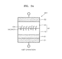
- FIG. 1 is a cross-sectional view illustrating a non-volatile memory element ME1 according to example embodiments of the present invention.
- the non-volatile memory element (hereinafter, referred to as a memory element) ME1 may include first and second electrodes E1 and E2 and a memory layer M1.
- the memory layer M1 may include a multi-layered structure disposed between the first and second electrodes E1 and E2.
- the memory layer M1 may be formed with a double-layered structure including a first material layer 10 and a second material layer 20.
- the memory layer M1 may have a resistance change characteristic due to movement of ionic species between the first material layer 10 and the second material layer 20.
- the first material layer 10 may be formed of a first metal oxide
- the second material layer 20 may be formed of a second metal oxide.
- an oxygen concentration may be changed gradually or regionally in a thickness direction in which the second material layer 20 is growing by a deposition process.
- a reaction-inhibiting layer B1 may be further included between the memory layer M1 and the first electrode E1. In other words, the reaction-inhibiting layer B1 may be placed between the first material layer 10 and the first electrode E1.
- the memory element ME1 according to example embodiments will be described in more detail.
- the first material layer 10 of the memory layer M1 may be formed of the first metal oxide.
- the first material layer 10 functions as an oxygen-supplying layer with respect to the second material layer 20.
- the first material layer 10 may be formed of one of Ta oxide, Zr oxide, yttria-stabilized zirconia (YSZ), Ti oxide, Hf oxide, Mn oxide, Mg oxide, and a combination thereof.
- the first material layer 10 may include TaO x , wherein 'x' may be less than about 2.5. Oxygen ions and/or oxygen vacancies may exist in the first material layer 10.
- a thickness of the first material layer 10 may be in the range of about several nanometers (nm) to about several hundred nanometers. As an example, the thickness of the first material layer 10 may be several tens of nm.
- the second material layer 20 may exchange oxygen ions and/or oxygen vacancies with the first material layer 10 and induce a resistance change of the memory layer M1.
- the second material layer 20 may be referred to as an oxygen exchange layer.
- the second material layer 20 may be an oxide layer having a multi-trap level (i.e., a plurality of trap levels).
- the trap and de-trap phenomenon of electrons are generally considered as one of the factors affecting a resistance value of the second material layer 20 at a high-resistance state.
- Factors affecting the high-resistance state of the second material layer 20 may include a thickness of the second material layer 20, positions of the traps, as well as, a trap level of the oxide.
- a shallow trap and a deep trap may be formed by the oxygen vacancies existing inside the oxide and by interstitial oxygen, and thus the resistance of the second material layer 20 at the high-resistance state may be increased.
- the resistance value of the second material layer 20 at the high-resistance state may be increased.
- the oxide having the multi-trap level can be an oxide including a plurality of oxidation states.
- the oxide with the multi-trap level may include one of Zr oxide, Mn oxide, Fe oxide, Mo oxide, Nb oxide, W oxide, Ln oxide, and a combination thereof which have a plurality of oxidation states.
- a thickness of the second material layer 20, which is formed of the oxide with a multi-trap level, may be in a range of about 5 to about 30 nm.
- an oxygen concentration in the second material layer 20 may be changed gradually or regionally in a thickness direction in which the second material layer 20 is growing by a deposition process.
- the oxygen concentration in the second material layer 20 may increase toward the second electrode E2.
- a ratio between O and Zr at a portion of the second material layer 20 interfacing with the first material layer 10 may be in the range of from about 1 to about 1.5, and the ratio between O and Zr at a portion of the second material layer 20 interfacing with the second electrode E2 may be about 2. This is the case illustrated in FIG. 2A .
- an oxygen concentration in the second material layer 20 may be changed regionally as illustrated in FIG. 2B .
- the second material layer 20 may include a first region (a lower portion) interfacing with the first material layer 10 and a second region (an upper portion) interfacing with the second electrode E2. Between the first and second regions, an oxygen concentration of the second region may be greater than that of the first region.
- a ratio between O and Zr in the first region adjacent to the first material layer 10 may be in a range of from about 1 to about 1.5, and the ratio between O and Zr in the second region adjacent to the second electrode E2 may be about 2. This is the case illustrated in FIG. 2B .
- a portion adjacent to the second electrode E2 of the second material layer 20 may have a stoichiometric composition or a composition close to the stoichiometric composition.
- a portion adjacent to the first material layer 10 of the second material layer 20 may have a non-stoichiometric composition. The portion adjacent to the first material layer 10 of the second material layer 20 may have a more significant affect on the resistance change of the memory layer M1 compared to the portion adjacent to the second electrode E2 of the second material layer 20.
- a resistance change characteristic of the memory element ME1 may be improved with the oxygen concentration variation in the second material layer 20 in the thickness direction in which the second material layer 20 is growing by a deposition process.
- the upper portion of the second material layer 20, which is interfacing with the second electrode E2 and having a stoichiometric composition or a composition close to the stoichiometric composition may increase a ratio between ON resistance and OFF resistance of the memory element ME1.
- the ON/OFF resistance ratio can be increased, because the upper portion of the second material layer 20 has a relatively high resistance compared to remaining regions and also separates the second electrode E2 from the lower portion of the second material layer 20 which is contributing to the resistance-change characteristic with exchange of ionic species. Accordingly, an OFF current level may be decreased, and thus the ON/OFF resistance ratio may be increased.
- the oxygen concentration variation in the second material layer 20 may further improve reliability, reproducibility, uniformity, as well, as stability of the memory element ME1.
- the upper portion of the second material layer 20, which interfaces with the second electrode E2 and has a stoichiometric composition or a composition close to the stoichiometric composition, may prevent or inhibit the remaining regions of the second material layer 20 from physically/chemically reacting with the second electrode E2 where the remaining regions substantially contribute to the resistance change characteristic.
- oxygen ions and/or oxygen vacancies of the second material layer 20 may move to the second electrode E2 and then physically/chemically react with the second electrode E2, or the second material layer 20 itself may physically/chemically react with the second electrode E2. Therefore, there may be deterioration of reliability, reproducibility, uniformity, and/or stability of the resistance-change characteristic of the memory element ME1.
- a region having a relatively high oxygen concentration with a stoichiometric composition (or a composition close to a stoichiometric composition) is formed in the portion interfacing with the second electrode E2 of the second material layer 20.
- the region having a relatively high oxygen concentration functions as a buffer so as to prevent or inhibit the remaining regions, which is substantially contributing to the resistance-change characteristic, from physically/chemically reacting with the second electrode E2.
- the region having a relatively high oxygen concentration of the second material layer 20 may be more stable than the remaining regions based on interatomic bonding energy. Accordingly, the region having a relatively high oxygen concentration in the second material layer 20 may increase a potential barrier between the remaining regions of the second material layer 20 and the second electrode E2. In other words, excessive current flow or movement of ionic species between the lower portion of the second material layer 20 and the second electrode E2 may be inhibited.
- the region having a relatively high oxygen concentration in the second material layer 20 may have a proper composition and thickness so as to function as a buffer while still allowing current flow.
- a thickness of the region having a relatively high oxygen concentration in the second material layer 20 may be less than about 20 nm.
- the remaining regions of the second material layer 20, that is, the region substantially contributing to the resistance-change characteristic may have a thickness of less than about 10 nm.
- the entire thickness of the second material layer 20 may be in the range of about 5 to about 30 nm.
- the second material layer 20 may be formed of a Zr oxide layer doped with a metal element such as Y, Sc, Ca, or La.
- the doping with the metal element may control an amount of the oxygen ions or oxygen vacancies in the second material layer 20 and may change charge mobility in the second material layer 20 as well.
- a doping concentration of the metal element may be or may not be uniform with regard to the second material layer 20 as a whole.
- the reaction-inhibiting layer B1 may be formed between the first electrode E1 and the first material layer 10.
- the reaction-inhibiting layer B1 inhibits physical/chemical reactions between the first electrode E1 and the first material layer 10, and thus may improve reliability, reproducibility, uniformity, and/or stability of the resistance-change characteristic of the memory layer M1.
- the reaction-inhibiting layer B1 may include a material having an interatomic bonding energy greater than that of the first material layer 10.
- the interatomic bonding energy in the reaction-inhibiting layer B1 may be greater than an interatomic bonding energy of Ta-O bonding.
- the reaction-inhibiting layer B1 may be formed of a material more stable than the material of the memory layer M1 in terms of the interatomic bonding energy.
- the reaction-inhibiting layer B1 may further include a material which may increase a potential barrier between the first electrode E1 and the first material layer 10.
- the conduction band offset between the reaction-inhibiting layer B1 and the first electrode E1 may be greater than the conduction band offset between the first material layer 10 and the first electrode E1.
- the reaction-inhibiting layer B1 may be formed of a material inhibiting an excessive current flow between the first electrode E1 and the first material layer 10.
- the reaction-inhibiting layer B1 may include a material having a resistivity greater than that of the first material layer 10.
- the reaction-inhibiting layer B1 may include at least one of AIO X , SiO x , SiN x , ZrO x , HfO x , and a combination thereof.
- the reaction-inhibiting layer B1 may or may not have a stoichiometric composition.
- the reaction-inhibiting layer B1 may have a proper composition and thickness to allow current flow while functioning as a buffer.
- a thickness of the reaction-inhibiting layer B1 may be less than about 10 nm.
- the thickness of the reaction-inhibiting layer B1 may be less than about 5 nm. If the reaction-inhibiting layer B1 is too thick, then an insulating property of the reaction-inhibiting layer B1 may be increased. Therefore, a proper thickness of the reaction-inhibiting layer B1 may be less than about 10 nm as described above.
- the first and second electrodes E1 and E2 may be formed of a non-precious metal (e.g., Ti, Ta, TiN, TiW, TaN, W, Ni, and Al), a relatively inexpensive precious metal (e.g., Ru), or an alloy thereof.
- the first and second electrodes E1 and E2 may also be formed of a conductive oxide.
- the conductive oxide may be a ZnO-based oxide (e.g., indium zinc oxide, IZO) or a SnO-based oxide (e.g., indium tin oxide, ITO).
- a stable memory characteristic may be obtained without employing first and second electrodes E1 and E2 formed from a relatively expensive precious metal, because the reaction-inhibiting layer B1 is used and the oxygen concentration in the second material layer 20 is changed in the thickness direction.
- the first and second electrodes E1 and E2 should be formed of a precious metal having a relatively low reactivity (which may be relatively expensive) in order to obtain a desired level of a memory characteristic.
- the use of a precious metal for the electrodes may increase the manufacturing cost of a memory device.
- the first and second electrodes E1 and E2 can be formed of a relatively low-priced material while obtaining reproducibility/stability of a memory characteristic with relative ease when there is an oxygen concentration variation in the second material layer 20 in the thickness direction and when the reaction-inhibiting layer B1 is used. It should be understood that a precious metal is not excluded as a material for forming the first and second electrodes E1 and E2 according to example embodiments.
- the first and second electrodes E1 and E2 may be formed of a precious metal (e.g., Pt, lr, Pd, or Au), when it is necessary. Therefore, the first and second electrodes E1 and E2 may include one of Pt, Ir, Pd, Au, Ru, Ti, Ta, TiN, TiW, TaN, W, Ni, Al, a conductive oxide and a combination thereof. In addition, the first and second electrodes E1 and E2 may be formed of various electrode materials which are generally used in a semiconductor device.
- a precious metal e.g., Pt, lr, Pd, or Au
- the first and second electrodes E1 and E2 may include one of Pt, Ir, Pd, Au, Ru, Ti, Ta, TiN, TiW, TaN, W, Ni, Al, a conductive oxide and a combination thereof.
- the first and second electrodes E1 and E2 may be formed of various electrode materials which are generally used in a semiconductor device.
- a positive voltage is applied to the first electrode E1 and a negative voltage is applied to the second electrode E2 during a set operation.
- oxygen vacancies may move from the first material layer 10 to the second material layer 20, and thus a current path (not shown) may be formed in the second material layer 20.
- a resistance of the memory layer M1 may be decreased, and the memory layer M1 may change from an OFF state to an ON state.
- oxygen ions may move in a direction opposite to the moving direction of the oxygen vacancies, that is, from the second material layer 20 to the first material layer 10.
- a negative voltage is applied to the first electrode E1 and a positive voltage is applied to the second electrode E2 during a reset operation.
- oxygen vacancies may move from the second material layer 20 to the first material layer 10
- oxygen ions may move from the first material layer 10 to the second material layer 20. Therefore, the current path (not shown) formed in the second material layer 20 may be broken. Accordingly, a resistance of the memory layer M1 may be increased, and thus the memory layer M1 may change from an ON state to an OFF state.
- the upper portion/region of the second material layer 20, which has a higher oxygen concentration, and the reaction-inhibiting layer B1 may function to improve stability, reliability and reproducibility of a resistance change characteristic during the set/reset operations.
- oxygen ions and/or oxygen vacancies related to a resistance change may move toward the first and second electrodes E1 and E2 during the set/reset operations.
- the oxygen ions and/or oxygen vacancies may physically/chemically react with the first and second electrodes E1 and E2, or the memory layer M1 itself may physically/chemically react with the first and second electrodes E1 and E2.
- the resistance change characteristic of the memory element ME1 may be deteriorated.
- a breakdown phenomenon may occur, in which an amount of current flow between the first electrode E1 and the second electrode E2 may be rapidly increased.
- an undesired material layer may be formed at interfaces between the memory layer M1 and each of the first and second electrodes E1 and E2 by a reaction therebetween, which may further deteriorate the resistance change characteristic.
- Such problems may be more serious when the first and second electrodes E1 and E2 are formed of an inexpensive non-precious metal.
- continuous ON/OFF switching operations may increase the possibility of the above noted problems.
- a resistance change characteristic can be significantly changed according to the method of forming the TaO x layer, the deposition condition, and the oxygen content.
- the reproducibility and stability of the resistance changed characteristics can be obtained while preventing the problems described previously when the reaction-inhibiting layer B1 is formed between the first electrode E1 and the memory layer M1, and a higher oxygen concentration region is formed in the upper portion of the second material layer 20, as described in example embodiments herein.
- the first and second electrodes E1 and E2 may be formed of a precious metal, a non-precious metal, and/or a conductive oxide. Without the higher oxygen concentration region in the second material layer 20 and the inclusion of the reaction-inhibiting layer B1, it may be relatively difficult to form the first and second electrodes E1 and E2 with a conductive oxide or a non-precious metal having a relatively high reactivity. Additionally, the use of a precious metal for the first and second electrodes E1 and E2 may increase a manufacturing cost of the device and may put various restrictions on the manufacturing process.
- the first and second electrodes E1 and E2 may be formed with relative ease not only of a precious metal but also of a non-precious metal and/or a conductive oxide.
- the manufacturing cost may be reduced, and there may also be various advantages to the manufacturing process.
- FIG. 4 is a graph showing variations of ON and OFF currents with the number of switching operations according to example embodiments.
- Fig. 4 is obtained with the memory element having a structure of W/Al 2 O 3 /TaO x /ZrO x /Ru.
- the memory element has the structure illustrated in FIG. 1 , and thus includes the first electrode E1, the reaction-inhibiting layer B1, the first material layer 10, the second material layer 20, and the second electrode E2, which are formed of W, Al 2 O 3 , TaO x , Zr , and Ru, respectively.
- the second material layer 20 formed of ZrO x an oxygen concentration is changed in a thickness direction in which the second material layer 20 is grown during a deposition process.
- a first graph G1 shows the variation of an ON current
- a second graph G2 shows the variation of the OFF current.
- the resistance change characteristic is relatively stable after repeating ON/OFF switching operations more than 10 6 times.
- a difference between the ON current and the OFF current is as large as about 4 to 5 orders of magnitude (i.e., about 10 4 to 10 5 ).
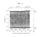
- FIG. 5 is a graph showing variations of the ON and OFF currents with the number of switching operations at various switching conditions in the non-limiting example embodiment having a structure of W/Al 2 O3/TaO x /ZrO x /Ru of FIG. 4 .
- Two different voltages i.e. "9V/-9V” and "11V/-11V" are applied to the memory element during various applied times (i.e., pulse widths).
- pulse widths i.e., 500 ns, 300 ns, 100 ns, and 50 ns.
- pulse widths e.g., 500 ns, 300 ns, 100 ns, and 50 ns.
- pulse widths e.g., 500 ns, 300 ns, 100 ns, and 50 ns.
- the applied voltage is "11V/-11V”
- each voltage pulse is applied during an applied time of 30 ns.
- the memory element when the applied voltage is "9V/-9V", an ON/OFF switching characteristic of the memory element is favorable even if the applied time for each voltage pulse is reduced to 50 ns. In addition, when the condition of an applied voltage is "11V/-11V", the ON/OFF switching characteristic is still favorable even if the applied time for each voltage pulse is shorter (e.g., 30 ns). Therefore, the memory element according to example embodiments has a significantly higher operation speed, compared to a conventional memory device such as a flash memory.
- the memory element has a relatively high operation speed and an advantageous ON/OFF switching characteristic if an oxygen concentration of a zirconium oxide layer (ZrO x ) is changed in the thickness direction of the second material layer 20 and if the reaction-inhibiting layer B1 formed of an Al 2 O 3 layer is present.
- ZrO x zirconium oxide layer
- the memory element according to example embodiments of the present invention may have an advantageous memory characteristic (e.g., a sufficient ON/OFF resistance ratio, a relatively high operation speed, etc.) and may have improved reliability, uniformity, and reproducibility.
- the manufacturing cost of the memory element may be reduced by using an inexpensive electrode material which may further provide advantages in the manufacturing process.
- the memory element may be used in memory devices having various structures.
- the memory device may further include a switching element connected to the memory element.
- FIG. 6 is a perspective view illustrating a memory device including the memory element of FIG. 1 , according to example embodiments of the present invention.
- the memory device may be a cross-point resistive memory device.
- a plurality of first wirings W1 may be formed parallel to one another in a first direction, e.g., in an X-direction.
- a plurality of second wirings W2 may be formed in a direction crossing the first wirings W1, e.g., in a Y-direction.
- Each of a plurality of first stack structures (first memory cell) SS1 may be formed in each cross-point between the first wirings W1 and the second wirings W2.
- the first stack structure SS1 may include a first reaction-inhibiting layer B1, a first memory layer M1, a first intermediate electrode N1, and a first switching element S1, that are sequentially stacked on the first wiring W1.
- the first memory layer M1 may include a first material layer 10 and a second material layer 20.
- the positions of the first memory layer M1 and the first switching element S1 may be switched.
- the position of the first reaction-inhibiting layer B1 may be changed to the side of the second wiring W2.
- the first reaction-inhibiting layer B1, the first material layer 10, and the second material layer 20 may correspond to the reaction-inhibiting layer B1, the first material layer 10, and the second material layer 20 of FIG. 1 , respectively.
- the first switching element S1 may be formed of a bi-directional diode, a threshold switching device, a varistor, or other suitable structure.
- the bi-directional diode may be an oxide diode.
- the silicon diode needs to be formed by a relatively high temperature process at a temperature of about 800°C. This relatively high temperature process may cause a restriction in selecting a substrate material and many other problems which may occur due to the relatively high temperature.
- the first switching element S1 is formed of an oxide layer which may be formed with relative ease at room temperature, various advantages may be obtained. As addressed above, the use of silicon may present some difficulties in the process, but it should be understood that a silicon material is not excluded as a material for forming the first switching element S1.
- the first switching element S1 may be formed of silicon or other qualified materials when it is desired.
- the first wiring W1 and first intermediate electrode N1 may correspond to the first electrode E1 and the second electrode E2 of FIG. 1 , respectively. Accordingly, at least one of the first wiring W1 and the first intermediate electrode N1 may include at least one of Pt, lr, Pd, Au, Ru, Ti, Ta, TiN, TiW, TaN, W, Ni, Al, a conductive oxide, and an alloy thereof.
- the second wiring W2 may be or may not be formed from the material which is used for the first wiring W1.
- a plurality of third wirings W3 may be further formed above upper surfaces of the second wirings W2.
- the plurality of third wings W3 are positioned parallel each other and spaced at a predetermined interval.
- the third wirings W3 may cross the second wirings W2 and may be arranged at the same interval with the first wirings W1.
- Each of a plurality of second stack structures (second memory cell) SS2 may be formed in each cross-point between the second wirings W2 and the third wirings W3.
- the second stack structure SS2 may include a second switching element S2, a second intermediate electrode N2, a second memory layer M2, and a second reaction-inhibiting layer B2 sequentially stacked on the second wiring W2.
- the second memory layer M2 may include a third material layer 30 and a fourth material layer 40.
- the positions of the second memory layer M2 and the second switching element S2 may be switched.
- the position of the second reaction-inhibiting layer B2 may be changed to the side of the second wiring W2.
- the second memory layer M2 may have a reversed structure relative to the first memory layer M1, meaning that the structure of the second memory layer M2 may be an mirror image of that of the first memory layer M1 along the second wiring W2.
- the third material layer 30 and the fourth material layer 40 of the second memory layer M2 may have an inversed structure relative to the second material layer 20 and the first material layer 10, respectively.
- the second memory layer M2 may have a stack structure that is the same as that of the first memory layer M1.
- the third material layer 30 and the fourth material layer 40 of the second memory layer M2 may correspond to the first material layer 10 and the second material layer 20 of the first memory layer M1, respectively.
- the second reaction-inhibiting layer B2 may be formed of a material which is used for the first reaction-inhibiting layer B1.
- the second reaction-inhibiting layer B2 may be disposed between the second intermediate electrode N2 and the second memory layer M2 instead of between the second memory layer M2 and the third wiring W3.
- the second switching element S2 may have an inversed structure of the first switching element S1 or a stack structure that is the same as the first switching element S1. In other words, a switching direction of the second switching element S2 may be opposite to or the same as that of the first switching element S1.
- the third wiring W3 and the second intermediate electrode N2 may correspond to the first electrode E1 and the second electrode E2 of FIG. 1 , respectively, or may correspond to the second electrode E2 and the first electrode E1 of FIG. 1 , respectively. Accordingly, at least one of the third wiring W3 and the second intermediate electrode N2 may include at least one of Pt, lr, Pd, Au, Ru, Ti, Ta, TiN, TiW, TaN, W, Ni, Al, a conductive oxide, and an alloy thereof.
- first and second stack structures SS1 and SS2 are illustrated as having a cylindrical column shape, but it should be understood that they may have other various shapes.
- the first and second stack structures SS1 and SS2 may have a square pillar shape or a pillar shape in which a width of the column increases in a downward direction.
- the first and second stack structures SS1 and SS2 may also have an asymmetrical shape.
- the first and/or second stack structures SS1 and SS2 may have a section with a cross-sectional area larger than an area of the cross-point formed by the neighboring wirings (e.g., W1 and W2, or W2 and W3).
- first and/or second stack structures SS1 and SS2 may have a portion whose center is off from the center of the cross-point formed by the neighboring wirings.
- the shape of the memory device illustrated in FIG. 6 may be further varied in accordance with the spirit and scope of the present invention.
- the memory device of FIG. 6 may further include an additional stack structure (not shown) on the third wiring W3.
- the additional stack structure may include a third stack structure and a fourth wiring which may be the same as the first stack structure SS1 and the second wiring W2, respectively.
- the memory device may further include yet another stack structure (not shown) on the additional stack structure.
- Such a stack structure may include a fourth stack structure and a fifth wiring which may be the same as the second stack structure SS2 and the third wiring W3, respectively.
Landscapes
- Chemical & Material Sciences (AREA)
- Crystallography & Structural Chemistry (AREA)
- Semiconductor Memories (AREA)
Applications Claiming Priority (1)
| Application Number | Priority Date | Filing Date | Title |
|---|---|---|---|
| KR1020100071611A KR20120010050A (ko) | 2010-07-23 | 2010-07-23 | 비휘발성 메모리요소 및 이를 포함하는 메모리소자 |
Publications (2)
| Publication Number | Publication Date |
|---|---|
| EP2410531A2 true EP2410531A2 (de) | 2012-01-25 |
| EP2410531A3 EP2410531A3 (de) | 2012-05-09 |
Family
ID=44645490
Family Applications (1)
| Application Number | Title | Priority Date | Filing Date |
|---|---|---|---|
| EP11173246A Withdrawn EP2410531A3 (de) | 2010-07-23 | 2011-07-08 | Nichtflüchtiges Speicherelement und Speichervorrichtung damit |
Country Status (4)
| Country | Link |
|---|---|
| US (1) | US8445882B2 (de) |
| EP (1) | EP2410531A3 (de) |
| KR (1) | KR20120010050A (de) |
| CN (1) | CN102347443B (de) |
Cited By (1)
| Publication number | Priority date | Publication date | Assignee | Title |
|---|---|---|---|---|
| EP2560171A3 (de) * | 2011-08-19 | 2014-11-26 | Samsung Electronics Co., Ltd. | Nichtflüchtige resistive Speicherelemente und Speichervorrichtungen damit |
Families Citing this family (19)
| Publication number | Priority date | Publication date | Assignee | Title |
|---|---|---|---|---|
| US8866121B2 (en) | 2011-07-29 | 2014-10-21 | Sandisk 3D Llc | Current-limiting layer and a current-reducing layer in a memory device |
| US8659001B2 (en) * | 2011-09-01 | 2014-02-25 | Sandisk 3D Llc | Defect gradient to boost nonvolatile memory performance |
| US8637413B2 (en) | 2011-12-02 | 2014-01-28 | Sandisk 3D Llc | Nonvolatile resistive memory element with a passivated switching layer |
| US8698119B2 (en) | 2012-01-19 | 2014-04-15 | Sandisk 3D Llc | Nonvolatile memory device using a tunnel oxide as a current limiter element |
| US8686386B2 (en) | 2012-02-17 | 2014-04-01 | Sandisk 3D Llc | Nonvolatile memory device using a varistor as a current limiter element |
| KR102010928B1 (ko) * | 2012-06-07 | 2019-10-21 | 삼성전자주식회사 | 저항 변화 메모리 장치, 그 동작 방법 및 제조 방법 |
| KR101929941B1 (ko) | 2012-08-10 | 2018-12-18 | 삼성전자 주식회사 | 저항 변화 물질 소자 및 이를 적용한 디바이스 |
| KR20140035558A (ko) | 2012-09-14 | 2014-03-24 | 삼성전자주식회사 | 가변 저항 메모리 장치 및 그 동작 방법 |
| US20140241031A1 (en) | 2013-02-28 | 2014-08-28 | Sandisk 3D Llc | Dielectric-based memory cells having multi-level one-time programmable and bi-level rewriteable operating modes and methods of forming the same |
| KR101481920B1 (ko) * | 2013-11-15 | 2015-01-14 | 포항공과대학교 산학협력단 | 금속-절연체 전이현상을 이용한 선택 소자, 및 이를 포함하는 비휘발성 메모리 셀 |
| US10424731B2 (en) | 2015-03-13 | 2019-09-24 | Toshiba Memory Corporation | Memory device |
| US9553132B1 (en) | 2015-09-09 | 2017-01-24 | Kabushiki Kaisha Toshiba | Semiconductor memory device |
| TWI553926B (zh) * | 2015-10-29 | 2016-10-11 | 華邦電子股份有限公司 | 電阻式記憶體及其製造方法 |
| CN109920908B (zh) * | 2017-12-13 | 2023-07-11 | 有研工程技术研究院有限公司 | 一种具有超薄转变功能层的阻变存储器及其制备方法 |
| KR102030341B1 (ko) * | 2018-12-19 | 2019-10-10 | 한양대학교 산학협력단 | 선택 소자 및 이를 이용한 메모리 소자 |
| US11404636B2 (en) * | 2020-04-24 | 2022-08-02 | Applied Materials, Inc | Crested barrier device and synaptic element |
| US12141688B2 (en) | 2020-04-24 | 2024-11-12 | Applied Materials, Inc. | Crested barrier device and synaptic element |
| CN111900248B (zh) * | 2020-07-06 | 2022-06-07 | 西安交通大学 | 一种基于电极堆栈的界面型多态阻变存储器及其制备方法 |
| KR20230062062A (ko) * | 2021-10-29 | 2023-05-09 | 에스케이하이닉스 주식회사 | 전자 장치 |
Citations (1)
| Publication number | Priority date | Publication date | Assignee | Title |
|---|---|---|---|---|
| JP2010021381A (ja) * | 2008-07-11 | 2010-01-28 | Panasonic Corp | 不揮発性記憶素子およびその製造方法、並びにその不揮発性記憶素子を用いた不揮発性半導体装置 |
Family Cites Families (10)
| Publication number | Priority date | Publication date | Assignee | Title |
|---|---|---|---|---|
| KR100693409B1 (ko) | 2005-01-14 | 2007-03-12 | 광주과학기술원 | 산화막의 저항변화를 이용한 비휘발성 기억소자 및 그제조방법 |
| US7569459B2 (en) * | 2006-06-30 | 2009-08-04 | International Business Machines Corporation | Nonvolatile programmable resistor memory cell |
| JP5010891B2 (ja) | 2006-10-16 | 2012-08-29 | 富士通株式会社 | 抵抗変化型素子 |
| KR100913395B1 (ko) | 2006-12-04 | 2009-08-21 | 한국전자통신연구원 | 메모리 소자 및 그 제조방법 |
| US8154003B2 (en) | 2007-08-09 | 2012-04-10 | Taiwan Semiconductor Manufacturing Company, Ltd. | Resistive non-volatile memory device |
| CN101828262B (zh) * | 2007-10-15 | 2012-06-06 | 松下电器产业株式会社 | 非易失性存储元件和使用该非易失性存储元件的非易失性半导体装置 |
| US8264865B2 (en) | 2008-07-11 | 2012-09-11 | Panasonic Corporation | Nonvolatile memory element, manufacturing method thereof, and nonvolatile semiconductor device incorporating nonvolatile memory element |
| JP4555397B2 (ja) * | 2008-08-20 | 2010-09-29 | パナソニック株式会社 | 抵抗変化型不揮発性記憶装置 |
| US8304754B2 (en) | 2008-11-12 | 2012-11-06 | Sandisk 3D Llc | Metal oxide materials and electrodes for Re-RAM |
| CN101621114A (zh) | 2009-07-21 | 2010-01-06 | 中国科学院上海硅酸盐研究所 | 一类氧化物多层梯度薄膜及其构建的rram元器件 |
-
2010
- 2010-07-23 KR KR1020100071611A patent/KR20120010050A/ko not_active Ceased
-
2011
- 2011-05-24 US US13/114,497 patent/US8445882B2/en active Active
- 2011-07-08 EP EP11173246A patent/EP2410531A3/de not_active Withdrawn
- 2011-07-14 CN CN201110197102.3A patent/CN102347443B/zh active Active
Patent Citations (1)
| Publication number | Priority date | Publication date | Assignee | Title |
|---|---|---|---|---|
| JP2010021381A (ja) * | 2008-07-11 | 2010-01-28 | Panasonic Corp | 不揮発性記憶素子およびその製造方法、並びにその不揮発性記憶素子を用いた不揮発性半導体装置 |
Cited By (1)
| Publication number | Priority date | Publication date | Assignee | Title |
|---|---|---|---|---|
| EP2560171A3 (de) * | 2011-08-19 | 2014-11-26 | Samsung Electronics Co., Ltd. | Nichtflüchtige resistive Speicherelemente und Speichervorrichtungen damit |
Also Published As
| Publication number | Publication date |
|---|---|
| CN102347443B (zh) | 2015-04-01 |
| US20120018695A1 (en) | 2012-01-26 |
| KR20120010050A (ko) | 2012-02-02 |
| CN102347443A (zh) | 2012-02-08 |
| US8445882B2 (en) | 2013-05-21 |
| EP2410531A3 (de) | 2012-05-09 |
Similar Documents
| Publication | Publication Date | Title |
|---|---|---|
| US8445882B2 (en) | Non-volatile memory element and memory device including the same | |
| US8772750B2 (en) | Non-volatile memory elements and memory devices including the same | |
| US7400027B2 (en) | Nonvolatile memory device having two or more resistance elements and methods of forming and using the same | |
| US7602042B2 (en) | Nonvolatile memory device, array of nonvolatile memory devices, and methods of making the same | |
| US9099639B2 (en) | Resistance switching material element and device employing the same | |
| EP2592624A2 (de) | Nichtflüchtige resistive metalldotierte Speicherelemente | |
| US20120032132A1 (en) | Nonvolatile Memory Elements And Memory Devices Including The Same | |
| US9484087B2 (en) | Multi-bit memory elements, memory devices including the same, and methods of manufacturing the same | |
| US9105837B2 (en) | Bipolar memory cells and memory devices including the same | |
| US20210384258A1 (en) | Three-dimensional resistive switching memory device and method of fabricating the same | |
| US20110161605A1 (en) | Memory devices and methods of operating the same | |
| EP2560171A2 (de) | Nichtflüchtige resistive Speicherelemente und Speichervorrichtungen damit | |
| US9000407B2 (en) | ReRAM materials stack for low-operating-power and high-density applications | |
| US20150137062A1 (en) | Mimcaps with quantum wells as selector elements for crossbar memory arrays | |
| US20160149129A1 (en) | Using Metal Silicides as Electrodes for MSM Stack in Selector for Non-Volatile Memory Application | |
| US8981327B1 (en) | Carbon-doped silicon based selector element | |
| US9373786B1 (en) | Two terminal resistive access devices and methods of formation thereof | |
| US9246092B1 (en) | Tunneling barrier creation in MSM stack as a selector device for non-volatile memory application | |
| US9443906B2 (en) | TiOx based selector element | |
| US9012878B1 (en) | MoOx based selector element | |
| US7518213B2 (en) | Nonvolatile variable resistance memory device and method of fabricating the same | |
| US8975610B1 (en) | Silicon based selector element | |
| KR101481920B1 (ko) | 금속-절연체 전이현상을 이용한 선택 소자, 및 이를 포함하는 비휘발성 메모리 셀 | |
| US9019744B2 (en) | Barrier design for steering elements | |
| US20150179934A1 (en) | ZrOx/STO/ZrOx Based Selector Element |
Legal Events
| Date | Code | Title | Description |
|---|---|---|---|
| AK | Designated contracting states |
Kind code of ref document: A2 Designated state(s): AL AT BE BG CH CY CZ DE DK EE ES FI FR GB GR HR HU IE IS IT LI LT LU LV MC MK MT NL NO PL PT RO RS SE SI SK SM TR |
|
| AX | Request for extension of the european patent |
Extension state: BA ME |
|
| PUAI | Public reference made under article 153(3) epc to a published international application that has entered the european phase |
Free format text: ORIGINAL CODE: 0009012 |
|
| PUAL | Search report despatched |
Free format text: ORIGINAL CODE: 0009013 |
|
| AK | Designated contracting states |
Kind code of ref document: A3 Designated state(s): AL AT BE BG CH CY CZ DE DK EE ES FI FR GB GR HR HU IE IS IT LI LT LU LV MC MK MT NL NO PL PT RO RS SE SI SK SM TR |
|
| AX | Request for extension of the european patent |
Extension state: BA ME |
|
| RIC1 | Information provided on ipc code assigned before grant |
Ipc: H01L 27/115 20060101ALI20120330BHEP Ipc: H01L 27/24 20060101ALI20120330BHEP Ipc: H01L 45/00 20060101ALI20120330BHEP Ipc: G11C 13/00 20060101AFI20120330BHEP |
|
| RAP1 | Party data changed (applicant data changed or rights of an application transferred) |
Owner name: SAMSUNG ELECTRONICS CO., LTD. |
|
| 17P | Request for examination filed |
Effective date: 20121109 |
|
| 17Q | First examination report despatched |
Effective date: 20130805 |
|
| STAA | Information on the status of an ep patent application or granted ep patent |
Free format text: STATUS: THE APPLICATION IS DEEMED TO BE WITHDRAWN |
|
| 18D | Application deemed to be withdrawn |
Effective date: 20131217 |