EP2410565A1 - Komponente zum Anschließen an eine Antenne - Google Patents
Komponente zum Anschließen an eine Antenne Download PDFInfo
- Publication number
- EP2410565A1 EP2410565A1 EP10170265A EP10170265A EP2410565A1 EP 2410565 A1 EP2410565 A1 EP 2410565A1 EP 10170265 A EP10170265 A EP 10170265A EP 10170265 A EP10170265 A EP 10170265A EP 2410565 A1 EP2410565 A1 EP 2410565A1
- Authority
- EP
- European Patent Office
- Prior art keywords
- conductor pattern
- component
- antenna
- contact
- embedded
- Prior art date
- Legal status (The legal status is an assumption and is not a legal conclusion. Google has not performed a legal analysis and makes no representation as to the accuracy of the status listed.)
- Withdrawn
Links
Images
Classifications
-
- H—ELECTRICITY
- H10—SEMICONDUCTOR DEVICES; ELECTRIC SOLID-STATE DEVICES NOT OTHERWISE PROVIDED FOR
- H10W—GENERIC PACKAGES, INTERCONNECTIONS, CONNECTORS OR OTHER CONSTRUCTIONAL DETAILS OF DEVICES COVERED BY CLASS H10
- H10W44/00—Electrical arrangements for controlling or matching impedance
- H10W44/20—Electrical arrangements for controlling or matching impedance at high-frequency [HF] or radio frequency [RF]
-
- G—PHYSICS
- G06—COMPUTING OR CALCULATING; COUNTING
- G06K—GRAPHICAL DATA READING; PRESENTATION OF DATA; RECORD CARRIERS; HANDLING RECORD CARRIERS
- G06K19/00—Record carriers for use with machines and with at least a part designed to carry digital markings
- G06K19/06—Record carriers for use with machines and with at least a part designed to carry digital markings characterised by the kind of the digital marking, e.g. shape, nature, code
- G06K19/067—Record carriers with conductive marks, printed circuits or semiconductor circuit elements, e.g. credit or identity cards also with resonating or responding marks without active components
- G06K19/07—Record carriers with conductive marks, printed circuits or semiconductor circuit elements, e.g. credit or identity cards also with resonating or responding marks without active components with integrated circuit chips
- G06K19/077—Constructional details, e.g. mounting of circuits in the carrier
- G06K19/07749—Constructional details, e.g. mounting of circuits in the carrier the record carrier being capable of non-contact communication, e.g. constructional details of the antenna of a non-contact smart card
- G06K19/0775—Constructional details, e.g. mounting of circuits in the carrier the record carrier being capable of non-contact communication, e.g. constructional details of the antenna of a non-contact smart card arrangements for connecting the integrated circuit to the antenna
- G06K19/07754—Constructional details, e.g. mounting of circuits in the carrier the record carrier being capable of non-contact communication, e.g. constructional details of the antenna of a non-contact smart card arrangements for connecting the integrated circuit to the antenna the connection being galvanic
-
- H—ELECTRICITY
- H10—SEMICONDUCTOR DEVICES; ELECTRIC SOLID-STATE DEVICES NOT OTHERWISE PROVIDED FOR
- H10W—GENERIC PACKAGES, INTERCONNECTIONS, CONNECTORS OR OTHER CONSTRUCTIONAL DETAILS OF DEVICES COVERED BY CLASS H10
- H10W70/00—Package substrates; Interposers; Redistribution layers [RDL]
- H10W70/60—Insulating or insulated package substrates; Interposers; Redistribution layers
- H10W70/611—Insulating or insulated package substrates; Interposers; Redistribution layers for connecting multiple chips together
-
- H—ELECTRICITY
- H10—SEMICONDUCTOR DEVICES; ELECTRIC SOLID-STATE DEVICES NOT OTHERWISE PROVIDED FOR
- H10W—GENERIC PACKAGES, INTERCONNECTIONS, CONNECTORS OR OTHER CONSTRUCTIONAL DETAILS OF DEVICES COVERED BY CLASS H10
- H10W70/00—Package substrates; Interposers; Redistribution layers [RDL]
- H10W70/60—Insulating or insulated package substrates; Interposers; Redistribution layers
- H10W70/611—Insulating or insulated package substrates; Interposers; Redistribution layers for connecting multiple chips together
- H10W70/614—Insulating or insulated package substrates; Interposers; Redistribution layers for connecting multiple chips together the multiple chips being integrally enclosed
-
- H—ELECTRICITY
- H10—SEMICONDUCTOR DEVICES; ELECTRIC SOLID-STATE DEVICES NOT OTHERWISE PROVIDED FOR
- H10W—GENERIC PACKAGES, INTERCONNECTIONS, CONNECTORS OR OTHER CONSTRUCTIONAL DETAILS OF DEVICES COVERED BY CLASS H10
- H10W70/00—Package substrates; Interposers; Redistribution layers [RDL]
- H10W70/60—Insulating or insulated package substrates; Interposers; Redistribution layers
- H10W70/62—Insulating or insulated package substrates; Interposers; Redistribution layers characterised by their interconnections
- H10W70/63—Vias, e.g. via plugs
- H10W70/635—Through-vias
-
- H—ELECTRICITY
- H10—SEMICONDUCTOR DEVICES; ELECTRIC SOLID-STATE DEVICES NOT OTHERWISE PROVIDED FOR
- H10W—GENERIC PACKAGES, INTERCONNECTIONS, CONNECTORS OR OTHER CONSTRUCTIONAL DETAILS OF DEVICES COVERED BY CLASS H10
- H10W70/00—Package substrates; Interposers; Redistribution layers [RDL]
- H10W70/60—Insulating or insulated package substrates; Interposers; Redistribution layers
- H10W70/699—Insulating or insulated package substrates; Interposers; Redistribution layers for flat cards, e.g. credit cards
-
- H—ELECTRICITY
- H05—ELECTRIC TECHNIQUES NOT OTHERWISE PROVIDED FOR
- H05K—PRINTED CIRCUITS; CASINGS OR CONSTRUCTIONAL DETAILS OF ELECTRIC APPARATUS; MANUFACTURE OF ASSEMBLAGES OF ELECTRICAL COMPONENTS
- H05K1/00—Printed circuits
- H05K1/18—Printed circuits structurally associated with non-printed electric components
- H05K1/182—Printed circuits structurally associated with non-printed electric components associated with components mounted in printed circuit boards [PCB], e.g. insert-mounted components [IMC]
- H05K1/185—Printed circuits structurally associated with non-printed electric components associated with components mounted in printed circuit boards [PCB], e.g. insert-mounted components [IMC] associated with components encapsulated in the insulating substrate of the PCBs; associated with components incorporated in internal layers of multilayer circuit boards
-
- H—ELECTRICITY
- H05—ELECTRIC TECHNIQUES NOT OTHERWISE PROVIDED FOR
- H05K—PRINTED CIRCUITS; CASINGS OR CONSTRUCTIONAL DETAILS OF ELECTRIC APPARATUS; MANUFACTURE OF ASSEMBLAGES OF ELECTRICAL COMPONENTS
- H05K2201/00—Indexing scheme relating to printed circuits covered by H05K1/00
- H05K2201/10—Details of components or other objects attached to or integrated in a printed circuit board
- H05K2201/10007—Types of components
- H05K2201/10098—Components for radio transmission, e.g. radio frequency identification [RFID] tag, printed or non-printed antennas
-
- H—ELECTRICITY
- H10—SEMICONDUCTOR DEVICES; ELECTRIC SOLID-STATE DEVICES NOT OTHERWISE PROVIDED FOR
- H10P—GENERIC PROCESSES OR APPARATUS FOR THE MANUFACTURE OR TREATMENT OF DEVICES COVERED BY CLASS H10
- H10P74/00—Testing or measuring during manufacture or treatment of wafers, substrates or devices
- H10P74/27—Structural arrangements therefor
- H10P74/273—Interconnections for measuring or testing, e.g. probe pads
-
- H—ELECTRICITY
- H10—SEMICONDUCTOR DEVICES; ELECTRIC SOLID-STATE DEVICES NOT OTHERWISE PROVIDED FOR
- H10W—GENERIC PACKAGES, INTERCONNECTIONS, CONNECTORS OR OTHER CONSTRUCTIONAL DETAILS OF DEVICES COVERED BY CLASS H10
- H10W44/00—Electrical arrangements for controlling or matching impedance
- H10W44/20—Electrical arrangements for controlling or matching impedance at high-frequency [HF] or radio frequency [RF]
- H10W44/241—Electrical arrangements for controlling or matching impedance at high-frequency [HF] or radio frequency [RF] for passive devices or passive elements
- H10W44/248—Electrical arrangements for controlling or matching impedance at high-frequency [HF] or radio frequency [RF] for passive devices or passive elements for antennas
-
- H—ELECTRICITY
- H10—SEMICONDUCTOR DEVICES; ELECTRIC SOLID-STATE DEVICES NOT OTHERWISE PROVIDED FOR
- H10W—GENERIC PACKAGES, INTERCONNECTIONS, CONNECTORS OR OTHER CONSTRUCTIONAL DETAILS OF DEVICES COVERED BY CLASS H10
- H10W72/00—Interconnections or connectors in packages
- H10W72/071—Connecting or disconnecting
- H10W72/072—Connecting or disconnecting of bump connectors
-
- H—ELECTRICITY
- H10—SEMICONDUCTOR DEVICES; ELECTRIC SOLID-STATE DEVICES NOT OTHERWISE PROVIDED FOR
- H10W—GENERIC PACKAGES, INTERCONNECTIONS, CONNECTORS OR OTHER CONSTRUCTIONAL DETAILS OF DEVICES COVERED BY CLASS H10
- H10W72/00—Interconnections or connectors in packages
- H10W72/071—Connecting or disconnecting
- H10W72/074—Connecting or disconnecting of anisotropic conductive adhesives
-
- H—ELECTRICITY
- H10—SEMICONDUCTOR DEVICES; ELECTRIC SOLID-STATE DEVICES NOT OTHERWISE PROVIDED FOR
- H10W—GENERIC PACKAGES, INTERCONNECTIONS, CONNECTORS OR OTHER CONSTRUCTIONAL DETAILS OF DEVICES COVERED BY CLASS H10
- H10W72/00—Interconnections or connectors in packages
- H10W72/20—Bump connectors, e.g. solder bumps or copper pillars; Dummy bumps; Thermal bumps
- H10W72/241—Dispositions, e.g. layouts
-
- H—ELECTRICITY
- H10—SEMICONDUCTOR DEVICES; ELECTRIC SOLID-STATE DEVICES NOT OTHERWISE PROVIDED FOR
- H10W—GENERIC PACKAGES, INTERCONNECTIONS, CONNECTORS OR OTHER CONSTRUCTIONAL DETAILS OF DEVICES COVERED BY CLASS H10
- H10W72/00—Interconnections or connectors in packages
- H10W72/20—Bump connectors, e.g. solder bumps or copper pillars; Dummy bumps; Thermal bumps
- H10W72/261—Functions other than electrical connecting
-
- H—ELECTRICITY
- H10—SEMICONDUCTOR DEVICES; ELECTRIC SOLID-STATE DEVICES NOT OTHERWISE PROVIDED FOR
- H10W—GENERIC PACKAGES, INTERCONNECTIONS, CONNECTORS OR OTHER CONSTRUCTIONAL DETAILS OF DEVICES COVERED BY CLASS H10
- H10W72/00—Interconnections or connectors in packages
- H10W72/30—Die-attach connectors
- H10W72/321—Structures or relative sizes of die-attach connectors
- H10W72/325—Die-attach connectors having a filler embedded in a matrix
-
- H—ELECTRICITY
- H10—SEMICONDUCTOR DEVICES; ELECTRIC SOLID-STATE DEVICES NOT OTHERWISE PROVIDED FOR
- H10W—GENERIC PACKAGES, INTERCONNECTIONS, CONNECTORS OR OTHER CONSTRUCTIONAL DETAILS OF DEVICES COVERED BY CLASS H10
- H10W72/00—Interconnections or connectors in packages
- H10W72/30—Die-attach connectors
- H10W72/351—Materials of die-attach connectors
- H10W72/352—Materials of die-attach connectors comprising metals or metalloids, e.g. solders
-
- H—ELECTRICITY
- H10—SEMICONDUCTOR DEVICES; ELECTRIC SOLID-STATE DEVICES NOT OTHERWISE PROVIDED FOR
- H10W—GENERIC PACKAGES, INTERCONNECTIONS, CONNECTORS OR OTHER CONSTRUCTIONAL DETAILS OF DEVICES COVERED BY CLASS H10
- H10W72/00—Interconnections or connectors in packages
- H10W72/30—Die-attach connectors
- H10W72/351—Materials of die-attach connectors
- H10W72/353—Materials of die-attach connectors not comprising solid metals or solid metalloids, e.g. ceramics
- H10W72/354—Materials of die-attach connectors not comprising solid metals or solid metalloids, e.g. ceramics comprising polymers
-
- H—ELECTRICITY
- H10—SEMICONDUCTOR DEVICES; ELECTRIC SOLID-STATE DEVICES NOT OTHERWISE PROVIDED FOR
- H10W—GENERIC PACKAGES, INTERCONNECTIONS, CONNECTORS OR OTHER CONSTRUCTIONAL DETAILS OF DEVICES COVERED BY CLASS H10
- H10W74/00—Encapsulations, e.g. protective coatings
- H10W74/10—Encapsulations, e.g. protective coatings characterised by their shape or disposition
- H10W74/15—Encapsulations, e.g. protective coatings characterised by their shape or disposition on active surfaces of flip-chip devices, e.g. underfills
-
- H—ELECTRICITY
- H10—SEMICONDUCTOR DEVICES; ELECTRIC SOLID-STATE DEVICES NOT OTHERWISE PROVIDED FOR
- H10W—GENERIC PACKAGES, INTERCONNECTIONS, CONNECTORS OR OTHER CONSTRUCTIONAL DETAILS OF DEVICES COVERED BY CLASS H10
- H10W90/00—Package configurations
- H10W90/701—Package configurations characterised by the relative positions of pads or connectors relative to package parts
- H10W90/721—Package configurations characterised by the relative positions of pads or connectors relative to package parts of bump connectors
- H10W90/724—Package configurations characterised by the relative positions of pads or connectors relative to package parts of bump connectors between a chip and a stacked insulating package substrate, interposer or RDL
Definitions
- the present invention relates to a component suitable for connection to an antenna.
- the invention relates for example to transmitter or receiver circuits, for example as provided in RFID devices.
- a component of this type includes an integrated circuit providing the receive and/or transmit functionality, and an antenna to receive or transmit signals.
- the antenna is formed on a substrate, which is, for instance, a plastic foil.
- the antenna usually is connected to the integrated circuit by means of contacts directly between the antenna coil and contact pads of the integrated circuit.
- the component may include a strap, also called an interposer, which is connected to the integrated circuit and to the antenna. Then, the antenna may be formed on a separate antenna substrate.
- the use of a strap/interposer helps to reduce the size of the electronics.
- the interposer includes conductive leads or pads that are electrically coupled to the contact pads of the integrated circuit for coupling to the antenna. These pads provide a larger effective electrical contact area to the antenna than IC pads which are precisely aligned for direct placement without an interposer. The larger area reduces the accuracy required for placement of the integrated circuit during manufacture, while still providing effective electrical connection.
- the larger area of the contact pads also increases the reliability of the connection between strap/interposer and antenna.
- the larger distance between the contact pads compared to the distance between the bumps of the IC makes the assembly easier as less placement accuracy is needed.
- Packaging techniques are known which provide a small microcircuit in a package and provide improved (and further apart) external contacts.
- the package around the semiconductor component thus facilitates its handling and connection.
- the surface of a package of a semiconductor component has contact parts, typically protrusions, which allow the packaged component to be easily installed on a circuit board.
- the package also contains internal conductors, through which signals can be routed to the actual microchip, connecting the protruding contact parts outside the package to the contact areas on the surface of the semiconductor component.
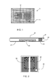
- FIG. 1 One example of the use of flip chip technology to connect an integrated circuit ("IC") to an antenna is shown in Figure 1 .
- the IC 10 is too small to provide connection lines that bridge the ends of the antenna coil 12, so it is not provided at the ends of the coil. Instead, the IC is connected in series along one line of the antenna coil.
- a separate bridge 14 connects the ends of the antenna coil, using a conductor path over an insulator layer. This requires high positional accuracy for the bare IC 10, and also requires additional processing and layers to provide the bridge across the coil ends.
- the distance between contact pads (bumps) may be less than 250 ⁇ m. This increases the cost of making connections between the component and other electric circuit elements, such as the antenna.
- the size of an antenna is limited by the electromagnetic performance required, so that the same degree of miniaturisation is not possible.
- the tolerance levels in the dimensions and positions of the connection points of the antenna are therefore larger, which can make connection to the miniaturised circuit a problem.
- a method of providing a microchip which is embedded in a base layer has been presented, for example in US2005/124148 .
- a surface of the base has contact areas which connect to the microchip.
- a problem with this design is that when connecting the base contact areas to an external component (such as an antenna) the pressure applied as part of the connection process can cause damage to the adjacent embedded microchip.
- a component comprising:
- both sides of the embedded integrated circuit structure enables the structure to implement a fan-out function to the opposite side of the component. This means that connections to external components are on the opposite side of the structure to the location of the integrated circuit, which means that better contact can be made (a higher pressure can be applied giving deeper imprinting).
- the set of vias and contact bumps typically comprises a plurality of vias and contact bumps, but is some examples there may be only one via and one contact bump in the set.
- the conductor pattern can comprise regions that connect with test pads of the integrated circuit. This can be used effectively to increase the size of the test pads, so that less precise test probes can be used.
- One or more analogue components can also be embedded in the insulator layer and making contact to the conductor pattern.
- the one or more analogue components can comprise a capacitor. This enables circuits to be formed with capacitances larger than possible only with a highly miniaturised integrated circuit.
- the component can further comprise a second set of contact bumps on the first side of the insulator.
- the invention also provides a device which comprises a component of the invention and an antenna connected to the set of contact bumps.
- the contact bumps can be positioned, shaped and sized to match the antenna pattern, so that the precision of the antenna pattern does not need to match the precision of the integrated circuit contact terminals.
- a component comprising:
- This arrangement provides the combined functions of a bridge (to cross multiple antenna coils) and contact between the IC and the antenna.
- the insulator layer is part of the component, so it can be directly placed over the antenna pattern using flip chip technology.
- the component can be combined with an antenna connected to the connection pads, wherein the antenna comprises a multiple turn spiral antenna pattern, wherein the connection pads connect to the ends of the spiral antenna pattern, with the insulator layer overlying one or more turns of the spiral pattern.
- the invention provides a component having an embedded IC in which the embedded package has a conductor pattern on one side which connects to the IC terminals, and a set of filled vias (outside the area where the integrated circuit is embedded), that connect between the conductor pattern and contact bumps on the opposite side of the embedded package.
- This double-sided package enables improved contact between the component and an antenna (for example).
- the component has an embedded IC in which the embedded package has a conductor pattern on one side which connects to the IC terminals.
- An insulator layer is provided over the conductor pattern over the region where the integrated circuit is situated, and connection pads of the conductor pattern extend beyond the insulator layer. This defines remote connection pads for connection to spaced antenna tracks and avoiding the need for an antenna bridge.
- Figure 2 shows one possible use of an embedded microchip which has been considered (but not published) by the applicant.
- the microchip 20 is embedded in a circuit board 22.
- Connection pads 24 are provided on the base, for connection to the antenna contacts.
- a through via 26 connects to a top electrode 28. The manufacturer can choose if they want to connect the component only on one side using both contacts 24, or on the top and bottom using the bottom left contact 24 and the top contact 28.
- the embedding process is well known.
- the microchip is embedded in a PCB laminate, or it may be embedded in thermo lasts (such as polycarbonate, or PETG).
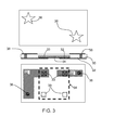
- Figure 3 shows a first example of component of the invention, in top view, cross sectional view and bottom view.
- the component comprises an embedded integrated circuit having a support structure 30 comprising an insulator layer, and a conductor pattern 32 on a first side of the insulator layer.
- the integrated circuit 34 is embedded in the insulator layer 30 and makes electrical contact with the conductor pattern 32 at its connection terminals 33.
- the insulator layer is preferably part of a laminate circuit board structure.
- the support 30 may be 200 ⁇ m thick, although thinner supports may be used in the future. Typically, the support may be between 100 ⁇ m and 300 ⁇ m thick.
- the IC 34 may be 75 ⁇ m thick, again with thickness likely to decrease to 50 ⁇ m or less in the future. Typically, the IC may be between 30 ⁇ m and 100 ⁇ m thick.
- the IC 34 is generally less than half as thick as the support.
- the metal contact layers are typically around 20 ⁇ m thick,
- FIG 3 shows that the integrated circuit 34 is not centrally embedded, but nearer the bottom face of the support 30 (i.e. the first side) than the opposite top face. This keeps the length of the contacts between the conductor pattern 32 and the terminals 33 as short as possible.
- IC can be placed in the middle of the package.
- the conductor pattern 32 extends beyond the outer area of the integrated circuit 34.
- a set of vias 36 is situated outside the area where the integrated circuit 34 is embedded and the vias each contact at one lower end with the conductor pattern 32.
- the other, top ends of the vias 36 connect to a second conductor pattern 38 in the form of a set of contact bumps.
- the contact bumps can take any size or shape, for example to match the antenna connection pads. Star shapes have been shown by way of random example.
- the integrated circuit also has test pads 39 to which no electrical connection is made.
- the purpose of the pattern 32 is to connect between the IC contact pads 33 and the vias 36 and any suitable shape may be used.
- the pattern 32 essentially provides a fan-out from the narrow IC contact terminals to more widely spaced contact bumps 38.
- the IC contact pads may be spaced by 250 ⁇ m (typically spaced in the range 100 ⁇ m to 1 mm), whereas the contact bumps will be typically spaced at least twice as far apart, for example in the range 1 mm to 10mm.
- the component is attached to the antenna upside down with respect to the design of Figure 2 .
- the external connections from the package are on the opposite side of the package to the first conductor pattern 32, and therefore on the opposite side with respect to the connection face of the integrated circuit.
- connection bumps 38 can be provided, and they can be spaced at any required distance by making the support of the embedded integrated circuit of suitable size.
- the electrical pads of the first conductor pattern 32 can also have large area, in that they can fan out to a large size once the pattern is beyond the integrated circuit boundary.
- the contact bumps can be optimised for the required external connection.
- a standard PCB manufacturing process is used, which has structured copper plates.
- the bumps can be copper (although optionally with coatings such as gold) for example for connection to copper antenna tracks.
- hard connection bumps can be used and with a large thickness.
- the bottom and top conductor patterns can be formed by a lamination process, which laminates the copper-insulator-copper plates.
- the component can be attached to the antenna using a conventional thermo-compression process, i.e. a flip chip bonding process.
- a standard flip chip assembly comprises:
- the pressure can be increased, the reliability of the connection is increased as the bumps can be imprinted deeper into the antenna material.
- a crimping process can be used, which is common for connecting two aluminium contacts by joining them together, to provide a good reliable connection.
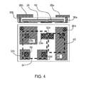
- Figure 4 shows a modification to the design of Figure 3 , in which the insulator layer 30 also embeds an additional component, for example an analogue component such as a capacitor 40.
- a portion 32a of the first conductor pattern 32 makes a connection between one of the contact pads 33a of the integrated circuit 34 and one terminal of the capacitor 40, and the other terminal of the capacitor connects through a via 36a to an upper contact bump 38a.
- the other contact pad 33b of the integrated circuit makes connection through a via 36b to the contact bump 38b.
- the miniaturisation of integrated circuits means the maximum capacitance which can be achieved within the chip is reduced.
- the arrangement of Figure 4 enables additional external capacitance to be added within the embedded structure.
- One terminal 33a of the IC connects to a contact bump 38a on the lower surface, and the other terminal 33b connects to a contact bump 38b on the upper surface.
- contact bumps 38a and 38b should be connected to the antenna. This design is suitable for a package which will be manually soldered, as the soldering process is easier.
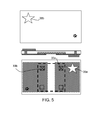
- Figure 6 shows another embodiment which does not require through vias.
- the figure shows a cross section and a view from beneath.
- the integrated circuit 34 connects to the first conductor pattern 32 as in the examples above.
- the two areas of the pattern 32 extend a long way to each side of the integrated circuit.
- a central area, beneath the integrated circuit 34, is covered by a second insulating layer 60 provided on the underside of the embedded integrated circuit.
- the insulator layer is thin compared to the other layers of the structure, for example 1 ⁇ m thick compared to 18-35 ⁇ m thickness of the electrode pattern 32.
- This arrangement can be used as a bridge at the ends of the antenna coil, but without requiring additional layers on the antenna foil.
- the insulator 50 covers the central antenna tracks, and the exposed parts of the conductor pattern 32 make contact to a respective end contact of the antenna. This is of particular interest for applications using coil shape antennas, such as high frequency applications.
- the invention makes use of an embedded integrated circuit approach, which offers a low cost packaging solution, for example less than 1 US Cent per mm 2 .
- the layout design is highly flexible, and the embedded package can be attached using existing equipment for direct chip attach, even though the chip size can be progressively reduced.
- Copper bumps can be used to improve the connection quality for a direct chip attach process.
- Coatings can also be used, for example a gold coating to improve connection reliability.
- the package can be bonded using standard flip chip assembly, for example with ACP (anisotropic conductive glue).
- ACP anisotropic conductive glue
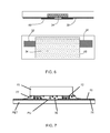
- the structure resulting from a standard flip chip assembly is shown in Figure 7 for an antenna with aluminium contacts.
- the package is shown as 70, with gold bumps (or gold coated copper bumps) 72. These are for contacting aluminium antenna tracks 74, having an aluminium oxide surface 76.
- the ACP 77 has conductive particles 78 which breach the aluminium oxide layer and make the contact.
- the antenna substrate is for example PET (Polyethylene terephthalate) with a PU (polyurethane) insulating coating.
- the ability to use higher pressures to imprint the contact bumps deep into the metal of the antenna means the conductive particles are no longer required.
- the bumps of the IC are normally 60x60 ⁇ m, whereas the contact bumps of the package of the invention can be significantly larger resulting in a larger contact area and therefore giving a better electrical connection.
- a non conductive glue can be used instead of the ACP.
- the structures underneath the bump of an embedded IC package are only capacitors, as bonding over active areas of the IC is forbidden, since during the assembly, the pressure on the bumps could damage the structures below.
- the design of the invention avoids any pressure on the bond pads of the IC, which gives more flexibility in the layout, and which can result in a smaller IC.
- the component enables the resolution requirements for the antenna to be relaxed.
- the main application of the invention is for the connection between a component having an IC and an antenna.
- the same principles can be used for the connection of the embedded IC package and any other external component.
Landscapes
- Engineering & Computer Science (AREA)
- Microelectronics & Electronic Packaging (AREA)
- Computer Hardware Design (AREA)
- Physics & Mathematics (AREA)
- General Physics & Mathematics (AREA)
- Theoretical Computer Science (AREA)
- Semiconductor Integrated Circuits (AREA)
Priority Applications (1)
| Application Number | Priority Date | Filing Date | Title |
|---|---|---|---|
| EP10170265A EP2410565A1 (de) | 2010-07-21 | 2010-07-21 | Komponente zum Anschließen an eine Antenne |
Applications Claiming Priority (1)
| Application Number | Priority Date | Filing Date | Title |
|---|---|---|---|
| EP10170265A EP2410565A1 (de) | 2010-07-21 | 2010-07-21 | Komponente zum Anschließen an eine Antenne |
Publications (1)
| Publication Number | Publication Date |
|---|---|
| EP2410565A1 true EP2410565A1 (de) | 2012-01-25 |
Family
ID=42371371
Family Applications (1)
| Application Number | Title | Priority Date | Filing Date |
|---|---|---|---|
| EP10170265A Withdrawn EP2410565A1 (de) | 2010-07-21 | 2010-07-21 | Komponente zum Anschließen an eine Antenne |
Country Status (1)
| Country | Link |
|---|---|
| EP (1) | EP2410565A1 (de) |
Cited By (5)
| Publication number | Priority date | Publication date | Assignee | Title |
|---|---|---|---|---|
| US8628018B2 (en) | 2012-04-17 | 2014-01-14 | Nxp, B.V. | RFID circuit and method |
| CN109166845A (zh) * | 2018-08-07 | 2019-01-08 | 清华大学 | 封装天线及其制造方法 |
| CN109244642A (zh) * | 2018-08-07 | 2019-01-18 | 清华大学 | 封装天线及其制造方法 |
| US10236260B2 (en) | 2016-06-30 | 2019-03-19 | Nxp Usa, Inc. | Shielded package with integrated antenna |
| WO2019065957A1 (ja) * | 2017-09-29 | 2019-04-04 | 株式会社村田製作所 | 無線通信デバイス |
Citations (6)
| Publication number | Priority date | Publication date | Assignee | Title |
|---|---|---|---|---|
| JP2003289128A (ja) * | 2002-01-23 | 2003-10-10 | Matsushita Electric Ind Co Ltd | 回路部品内蔵モジュールおよびその製造方法 |
| US20050124148A1 (en) | 2002-01-31 | 2005-06-09 | Tuominen Risto | Method for embedding a component in a base and forming a contact |
| US20050184377A1 (en) * | 2004-01-30 | 2005-08-25 | Shinko Electric Industries Co., Ltd. | Semiconductor device and method of manufacturing the same |
| WO2008057895A1 (en) * | 2006-11-08 | 2008-05-15 | Atmel Corporation | Multi-component electronic package with planarized embedded-components substrate |
| US20080186690A1 (en) * | 2007-02-07 | 2008-08-07 | Nokia Corporation | Electronics Package And Manufacturing Method Thereof |
| US20090293271A1 (en) * | 2008-06-02 | 2009-12-03 | Ibiden Co., Ltd. | Printed wiring board with built-in electronic component and manufacturing method thereof |
-
2010
- 2010-07-21 EP EP10170265A patent/EP2410565A1/de not_active Withdrawn
Patent Citations (6)
| Publication number | Priority date | Publication date | Assignee | Title |
|---|---|---|---|---|
| JP2003289128A (ja) * | 2002-01-23 | 2003-10-10 | Matsushita Electric Ind Co Ltd | 回路部品内蔵モジュールおよびその製造方法 |
| US20050124148A1 (en) | 2002-01-31 | 2005-06-09 | Tuominen Risto | Method for embedding a component in a base and forming a contact |
| US20050184377A1 (en) * | 2004-01-30 | 2005-08-25 | Shinko Electric Industries Co., Ltd. | Semiconductor device and method of manufacturing the same |
| WO2008057895A1 (en) * | 2006-11-08 | 2008-05-15 | Atmel Corporation | Multi-component electronic package with planarized embedded-components substrate |
| US20080186690A1 (en) * | 2007-02-07 | 2008-08-07 | Nokia Corporation | Electronics Package And Manufacturing Method Thereof |
| US20090293271A1 (en) * | 2008-06-02 | 2009-12-03 | Ibiden Co., Ltd. | Printed wiring board with built-in electronic component and manufacturing method thereof |
Cited By (7)
| Publication number | Priority date | Publication date | Assignee | Title |
|---|---|---|---|---|
| US8628018B2 (en) | 2012-04-17 | 2014-01-14 | Nxp, B.V. | RFID circuit and method |
| US10236260B2 (en) | 2016-06-30 | 2019-03-19 | Nxp Usa, Inc. | Shielded package with integrated antenna |
| WO2019065957A1 (ja) * | 2017-09-29 | 2019-04-04 | 株式会社村田製作所 | 無線通信デバイス |
| JPWO2019065957A1 (ja) * | 2017-09-29 | 2019-11-14 | 株式会社村田製作所 | 無線通信デバイス |
| US11114392B2 (en) | 2017-09-29 | 2021-09-07 | Murata Manufacturing Co., Ltd. | Wireless communication device |
| CN109166845A (zh) * | 2018-08-07 | 2019-01-08 | 清华大学 | 封装天线及其制造方法 |
| CN109244642A (zh) * | 2018-08-07 | 2019-01-18 | 清华大学 | 封装天线及其制造方法 |
Similar Documents
| Publication | Publication Date | Title |
|---|---|---|
| US7728422B2 (en) | Semiconductor package, integrated circuit cards incorporating the semiconductor package, and method of manufacturing the same | |
| US6815254B2 (en) | Semiconductor package with multiple sides having package contacts | |
| EP3007102B1 (de) | Halbleiterbauelement und verfahren zur herstellung eines halbleiterbauelements | |
| US20120153432A1 (en) | Semiconductor device and method for manufacturing same | |
| KR101417881B1 (ko) | 전자 부품 내장 기판 | |
| EP2410565A1 (de) | Komponente zum Anschließen an eine Antenne | |
| CN106470527A (zh) | 用于形成增强型指纹辨识模块的印刷电路板结构 | |
| KR20160091493A (ko) | 지문센서 모듈 및 이의 제조방법 | |
| KR100818088B1 (ko) | 반도체 패키지 및 그 제조 방법 | |
| KR101096330B1 (ko) | 반도체 장치용 패키지 | |
| EP2013906B1 (de) | Mikrowellenchip-Trägerstruktur | |
| US20110073357A1 (en) | Electronic device and method of manufacturing an electronic device | |
| US12380311B2 (en) | Articles of manufacture relating to IC modules and smart cards | |
| KR20170126336A (ko) | 지문인식센서 패키지 및 그 제조 방법 | |
| KR100923542B1 (ko) | 이형재를 이용한 임베디드 반도체 패키지 장치 및 그 제조 방법 | |
| US8830690B2 (en) | Minimizing plating stub reflections in a chip package using capacitance | |
| AU2023433488B2 (en) | Articles of manufacture relating to ic modules and smart cards | |
| KR100926088B1 (ko) | 카트리지를 이용한 임베디드 반도체 패키지 및 그 제조 방법 | |
| Yacoub-George et al. | Ultra-thin flexible interposer-a flexible hybrid integration approach to replace wire bonds | |
| KR20130076900A (ko) | 전자부품 실장구조 중간체, 전자부품 실장구조체 및 전자부품 실장구조체의 제조방법 | |
| KR101004897B1 (ko) | 멀티 칩 모듈 패키지 | |
| HK40119002A (en) | Articles of manufacture relating to ic modules and smart cards | |
| HK40119002B (en) | Articles of manufacture relating to ic modules and smart cards | |
| KR101664476B1 (ko) | 통신모듈 | |
| KR20120008952A (ko) | 칩 패키지용 면상 부재 및 이를 이용한 칩 패키지 및 칩 패키지용 면상 부재 제조 방법 |
Legal Events
| Date | Code | Title | Description |
|---|---|---|---|
| AK | Designated contracting states |
Kind code of ref document: A1 Designated state(s): AL AT BE BG CH CY CZ DE DK EE ES FI FR GB GR HR HU IE IS IT LI LT LU LV MC MK MT NL NO PL PT RO SE SI SK SM TR |
|
| AX | Request for extension of the european patent |
Extension state: BA ME RS |
|
| PUAI | Public reference made under article 153(3) epc to a published international application that has entered the european phase |
Free format text: ORIGINAL CODE: 0009012 |
|
| STAA | Information on the status of an ep patent application or granted ep patent |
Free format text: STATUS: THE APPLICATION IS DEEMED TO BE WITHDRAWN |
|
| 18D | Application deemed to be withdrawn |
Effective date: 20120726 |