EP2410817A2 - Circuit de commande de dispositif électroluminescent - Google Patents
Circuit de commande de dispositif électroluminescent Download PDFInfo
- Publication number
- EP2410817A2 EP2410817A2 EP10186773A EP10186773A EP2410817A2 EP 2410817 A2 EP2410817 A2 EP 2410817A2 EP 10186773 A EP10186773 A EP 10186773A EP 10186773 A EP10186773 A EP 10186773A EP 2410817 A2 EP2410817 A2 EP 2410817A2
- Authority
- EP
- European Patent Office
- Prior art keywords
- light emitting
- emitting device
- voltage
- unit
- driving circuit
- Prior art date
- Legal status (The legal status is an assumption and is not a legal conclusion. Google has not performed a legal analysis and makes no representation as to the accuracy of the status listed.)
- Granted
Links
- 239000003990 capacitor Substances 0.000 claims description 5
- 230000005669 field effect Effects 0.000 claims description 2
- 239000004065 semiconductor Substances 0.000 claims description 2
- 230000002708 enhancing effect Effects 0.000 description 2
- 238000000034 method Methods 0.000 description 2
- 230000004075 alteration Effects 0.000 description 1
- 230000000694 effects Effects 0.000 description 1
- 238000012986 modification Methods 0.000 description 1
- 230000004048 modification Effects 0.000 description 1
- 239000002699 waste material Substances 0.000 description 1
Images


Classifications
-
- H—ELECTRICITY
- H05—ELECTRIC TECHNIQUES NOT OTHERWISE PROVIDED FOR
- H05B—ELECTRIC HEATING; ELECTRIC LIGHT SOURCES NOT OTHERWISE PROVIDED FOR; CIRCUIT ARRANGEMENTS FOR ELECTRIC LIGHT SOURCES, IN GENERAL
- H05B45/00—Circuit arrangements for operating light-emitting diodes [LED]
- H05B45/40—Details of LED load circuits
- H05B45/44—Details of LED load circuits with an active control inside an LED matrix
- H05B45/48—Details of LED load circuits with an active control inside an LED matrix having LEDs organised in strings and incorporating parallel shunting devices
-
- H—ELECTRICITY
- H05—ELECTRIC TECHNIQUES NOT OTHERWISE PROVIDED FOR
- H05B—ELECTRIC HEATING; ELECTRIC LIGHT SOURCES NOT OTHERWISE PROVIDED FOR; CIRCUIT ARRANGEMENTS FOR ELECTRIC LIGHT SOURCES, IN GENERAL
- H05B45/00—Circuit arrangements for operating light-emitting diodes [LED]
- H05B45/40—Details of LED load circuits
- H05B45/44—Details of LED load circuits with an active control inside an LED matrix
-
- H—ELECTRICITY
- H05—ELECTRIC TECHNIQUES NOT OTHERWISE PROVIDED FOR
- H05B—ELECTRIC HEATING; ELECTRIC LIGHT SOURCES NOT OTHERWISE PROVIDED FOR; CIRCUIT ARRANGEMENTS FOR ELECTRIC LIGHT SOURCES, IN GENERAL
- H05B45/00—Circuit arrangements for operating light-emitting diodes [LED]
- H05B45/40—Details of LED load circuits
-
- H—ELECTRICITY
- H05—ELECTRIC TECHNIQUES NOT OTHERWISE PROVIDED FOR
- H05B—ELECTRIC HEATING; ELECTRIC LIGHT SOURCES NOT OTHERWISE PROVIDED FOR; CIRCUIT ARRANGEMENTS FOR ELECTRIC LIGHT SOURCES, IN GENERAL
- H05B47/00—Circuit arrangements for operating light sources in general, i.e. where the type of light source is not relevant
- H05B47/10—Controlling the light source
-
- Y—GENERAL TAGGING OF NEW TECHNOLOGICAL DEVELOPMENTS; GENERAL TAGGING OF CROSS-SECTIONAL TECHNOLOGIES SPANNING OVER SEVERAL SECTIONS OF THE IPC; TECHNICAL SUBJECTS COVERED BY FORMER USPC CROSS-REFERENCE ART COLLECTIONS [XRACs] AND DIGESTS
- Y02—TECHNOLOGIES OR APPLICATIONS FOR MITIGATION OR ADAPTATION AGAINST CLIMATE CHANGE
- Y02B—CLIMATE CHANGE MITIGATION TECHNOLOGIES RELATED TO BUILDINGS, e.g. HOUSING, HOUSE APPLIANCES OR RELATED END-USER APPLICATIONS
- Y02B20/00—Energy efficient lighting technologies, e.g. halogen lamps or gas discharge lamps
- Y02B20/30—Semiconductor lamps, e.g. solid state lamps [SSL] light emitting diodes [LED] or organic LED [OLED]
Definitions
- the present invention relates to a light emitting device driving circuit, and particularly to a light emitting device driving circuit comprising a reverse voltage providing unit, where the total operating voltage of the light emitting device can be reduced in correspondence to the reverse voltage provided by the reverse voltage providing unit, thus enhancing the efficiency and the power factor of the light emitting device.
- a driving circuit for light emitting diodes raises the operating voltage of the LEDs to enhance the efficiency.
- the voltage of alternate current power is in the form of a sine wave, and raising the operating voltage of the LEDs would lead to a reduction of the power factor of the driving circuit. Once the power factor is reduced, power waste exists, which is in contradiction to the well-recognized concept to save energy.
- the power factor can be increased by lowering the operating voltage of the LEDs. By doing this, however, the voltage drop between the power source and the LEDs would increase, thus reducing the overall efficiency of the circuits.
- the inventor focuses on a new invention of a light emitting device driving circuit.
- An objective of the present invention is to provide a light emitting device driving circuit in order to achieve a stabilized light emitting device driving circuit with high efficiency and high power factor.
- the invention provides a light emitting device driving circuit, which comprises a rectification unit, a current limiting unit and a load.
- the load comprises a first light emitting device, a reverse voltage providing unit and a second light emitting device connected in serial.
- the rectification unit is configured to rectify an alternate current voltage from an outside power source to output a direct current voltage.
- the current limiting unit is electrically connected to the rectification unit and generates a direct current corresponding to the direct current voltage.
- the load is connected between the current limiting unit and the rectification unit.
- the reverse voltage providing unit provides a reverse voltage, the reverse voltage having an opposite polarity to the voltage drop.
- the total operating voltage of the light emitting devices is reduced, thus enhancing the efficiency and the power factor of the light emitting devices.
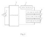
- Fig. 1 is a schematic view of a light emitting device driving circuit according to an embodiment of the invention
- Fig. 2 is a schematic view of a light emitting device driving circuit according to another embodiment of the invention.
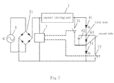
- Fig. 3 is a schematic view of a light emitting device driving circuit according to a further embodiment of the invention.
- Fig. 4 is a schematic view of a light emitting device driving circuit according to a further embodiment of the invention.
- Fig. 1 is a schematic view of a light emitting device driving circuit according to an embodiment of the invention.
- the invention is a light emitting device driving circuit, which comprises a rectification unit 2, a current limiting unit 3 and a load.
- the load has a first light emitting device 4, a reverse voltage providing unit 6 and a second light emitting device 5 connected in serial. Details of the electrical connections of the elements are shown in Fig. 1 and are hereby omitted.
- the rectification unit 2 is configured to rectify an alternate current voltage from an outside power source 1 to output a direct current voltage.
- the current limiting unit 3 is electrically connected to the rectification unit 2 and generates a direct current corresponding to the direct current voltage for driving the first light emitting device 4 and the second light emitting device 5.
- the first light emitting device 4 and the second light emitting device 5 are preferably organic light emitting diodes (OLEDs), light emitting diodes (LEDs) or electroluminescent light emitting devices, and in this embodiment LEDs are used as examples.
- the reverse voltage providing unit 6 provides a reverse voltage, in which the reverse voltage has an opposite polarity to the voltage drop.
- the reverse voltage providing unit is preferably a primary battery.
- the direct current power rectified by the rectification unit 2 and limited by the current limiting unit 3, is provided to the first light emitting device 4 and the second light emitting device 5 for emitting light.
- the output current equals the input current, and the output voltage is the total voltage drop of the first light emitting device 4, the reverse voltage providing unit 6 and the second light emitting device 5.
- the reverse voltage provided by the reverse voltage providing unit 6 may increase the LED efficiency and the power factor.
- FIG. 2 is a schematic view of a light emitting device driving circuit according to another embodiment of the invention.
- the embodiment comprises a rectification unit 2, a current limiting unit 3, a first light emitting device 41, a primary battery 61 and a second light emitting device 51.
- the rectification unit 2 and the current limiting unit 3 are electrically connected, and the other end of the current limiting unit 3 and the first light emitting device 41 are electrically connected.
- the two ends of the primary battery 61 are connected to the first light emitting device 41 and the second light emitting device 51.
- the second light emitting device 51 is electrically connected to the rectification unit 2.
- the alternate current source 1 provides direct current power, which is rectified by the rectification unit 2 and limited by the current limiting unit 3, and then provided to the first light emitting device 41 and the second light emitting device 51 for emitting light.
- the primary battery 61 provides a reverse voltage to reduce the total voltage difference of the load, and increase the LED efficiency and the power factor.
- FIG. 3 is a schematic view of a light emitting device driving circuit according to a further embodiment of the invention.
- the embodiment comprises a rectification unit 2, a current limiting unit 3, a first light emitting device 41, a second light emitting device 51, a capacitance 62, a diode 63, a control unit 7, a first switch 71 and a second switch 72.
- the rectification unit 2 in this embodiment is a bridge rectifier 21, and the control unit 7 is provided for detecting the voltage of the bridge rectifier 21 and controlling the first switch 71 and the second switch 72.
- the bridge rectifier 21 and the current limiting unit 3 are electrically connected, and the other end of the current limiting unit 3 is electrically connected to the first light emitting device 41 and the first switch 71.
- the first light emitting device 41 is electrically connected to the capacitor 62, the diode 63 and the second switch 72 at a first node.
- One end of the second light emitting device 51 is electrically connected to the capacitor 62, the diode 63 and the first switch 71 at a second node.
- the other end of the second light emitting device 51 is electrically connected to the bridge rectifier 21.
- the control unit 7 is electrically connected to the bridge rectifier 21 and, respectively, to the first switch 71 and the second switch 72, for detecting the direct current voltage output by the bridge rectifier 21 and controlling the first switch 71 and the second switch 72 corresponding to the direct current voltage.
- the alternate current voltage is provided as a sine wave.
- the control unit 7 detects the voltage V generated by the bridge rectifier 21.
- the control unit 7 When the voltage V is lower than a predetermined voltage value Vs (V ⁇ Vs), the control unit 7 generates a signal to switch off the first switch 71 and the second switch 72 to create conductance, thus the current flows to the capacitor 62 for electric power storage.
- the control unit 7 When the voltage V is higher than the predetermined voltage value Vs (V > Vs), the control unit 7 generates a signal to switch on the first switch 71 and the second switch 72 to create an open circuit, thus the current flows to the first light emitting device 41 and the second light emitting device 51.
- the capacitor 62 with electric power stored therein generates a reverse voltage to reduce the total voltage difference of the load, and increase the LED efficiency and the power factor.
- the first switch 71 and the second switch 72 can be metal-oxide-semiconductor field-effect transistors (MOSFETs), relays or bipolar junction transistors (BJTs), and in this embodiment the MOSFETs are used as the examples.
- the control unit 7 changes the gate voltage of the MOSFETs in correspondence to the detected direct current voltage, thus controlling the conductance or the open circuit of the MOSFETs.
- FIG. 4 is a schematic view of a light emitting device driving circuit according to a further embodiment of the invention.
- the embodiment comprises a rectification unit 2, a current limiting unit 3, a first light emitting device 41, a second light emitting device 51, a secondary battery 64, a diode 63, a control unit 7, a first switch 71 and a second switch 72.
- the control unit 7 is provided for detecting the voltage of the rectification unit 2 and controlling the first switch 71 and the second switch 72.
- the rectification unit 2 and the current limiting unit 3 are electrically connected, and the other end of the current limiting unit 3 is electrically connected to the first light emitting device 41 and the first switch 71.
- the first light emitting device 41 is electrically connected to the secondary battery 64, the diode 63 and the second switch 72 at a first node.
- One end of the second light emitting device 51 is electrically connected to the secondary battery 64, the diode 63 and the first switch 71 at a second node.
- the other end of the second light emitting device 51 is electrically connected to the rectification unit 2.
- the control unit 7 is electrically connected to the rectification unit 2 and, respectively, to the first switch 71 and the second switch 72, for detecting the direct current voltage output by the rectification unit 2 and controlling the first switch 71 and the second switch 72 corresponding to the direct current voltage .
- the alternate current voltage is provided as a sine wave.
- the control unit 7 detects the voltage V generated by the rectification unit 2.
- V ⁇ Vs a predetermined voltage value
- the control unit 7 When the voltage V is lower than a predetermined voltage value Vs (V ⁇ Vs), the control unit 7 generates a signal to switch off the first switch 71 and the second switch 72 to create conductance, thus the current flows to the secondary battery 64 for electric power storage.
- Vs voltage higher than the predetermined voltage value Vs (V > Vs)
- the control unit 7 generates a signal to switch on the first switch 71 and the second switch 72 to create an open circuit, thus the current flows to the first light emitting device 41 and the second light emitting device 51.
- the secondary battery 64 with electric power stored therein generates a reverse voltage to reduce the total voltage difference of the load, and increase the LED efficiency and the power factor.
Landscapes
- Circuit Arrangement For Electric Light Sources In General (AREA)
- Dc-Dc Converters (AREA)
- Rectifiers (AREA)
- Led Devices (AREA)
Applications Claiming Priority (1)
| Application Number | Priority Date | Filing Date | Title |
|---|---|---|---|
| TW099124397A TWI434599B (zh) | 2010-07-23 | 2010-07-23 | A light-emitting element driving circuit |
Publications (3)
| Publication Number | Publication Date |
|---|---|
| EP2410817A2 true EP2410817A2 (fr) | 2012-01-25 |
| EP2410817A3 EP2410817A3 (fr) | 2014-05-21 |
| EP2410817B1 EP2410817B1 (fr) | 2015-09-16 |
Family
ID=45090791
Family Applications (1)
| Application Number | Title | Priority Date | Filing Date |
|---|---|---|---|
| EP10186773.7A Active EP2410817B1 (fr) | 2010-07-23 | 2010-10-06 | Circuit de commande de dispositif électroluminescent |
Country Status (6)
| Country | Link |
|---|---|
| US (1) | US8410710B2 (fr) |
| EP (1) | EP2410817B1 (fr) |
| JP (1) | JP5179548B2 (fr) |
| KR (1) | KR101171042B1 (fr) |
| AU (1) | AU2010230081B2 (fr) |
| TW (1) | TWI434599B (fr) |
Cited By (1)
| Publication number | Priority date | Publication date | Assignee | Title |
|---|---|---|---|---|
| WO2013150399A1 (fr) * | 2012-03-20 | 2013-10-10 | Koninklijke Philips N.V. | Circuit de pilotage de chaîne de del contenant une diode de commande de charge pour un condensateur |
Families Citing this family (8)
| Publication number | Priority date | Publication date | Assignee | Title |
|---|---|---|---|---|
| TW201401920A (zh) * | 2012-06-22 | 2014-01-01 | Jinone Inc | 穩定發光之led裝置 |
| JP6013809B2 (ja) * | 2012-07-05 | 2016-10-25 | ローム株式会社 | Ledドライバ回路および照明装置 |
| US9528210B2 (en) | 2013-10-31 | 2016-12-27 | Kimberly-Clark Worldwide, Inc. | Method of making a dispersible moist wipe |
| US10113254B2 (en) | 2013-10-31 | 2018-10-30 | Kimberly-Clark Worldwide, Inc. | Dispersible moist wipe |
| US9005395B1 (en) | 2014-01-31 | 2015-04-14 | Kimberly-Clark Worldwide, Inc. | Dispersible hydroentangled basesheet with triggerable binder |
| US9414452B1 (en) * | 2015-01-16 | 2016-08-09 | Iml International | Light-emitting diode lighting device with synchronized PWM dimming control |
| US10467220B2 (en) * | 2015-02-19 | 2019-11-05 | Medidata Solutions, Inc. | System and method for generating an effective test data set for testing big data applications |
| WO2017179661A1 (fr) * | 2016-04-15 | 2017-10-19 | 日立化成株式会社 | Matériau de transport de charge, composition d'encre utilisant ledit matériau, élément électronique organique, élément électroluminescent organique, élément d'affichage, dispositif d'éclairage et dispositif d'affichage |
Family Cites Families (15)
| Publication number | Priority date | Publication date | Assignee | Title |
|---|---|---|---|---|
| US4503390A (en) * | 1981-05-07 | 1985-03-05 | Ideal Industries, Inc. | Switchless voltage, continuity and polarity indicator |
| US6020735A (en) * | 1998-04-24 | 2000-02-01 | Lucent Technologies Inc. | Switching device internal diode detection circuit and method of operating the same |
| JP3416082B2 (ja) * | 1999-07-01 | 2003-06-16 | 株式会社松村電機製作所 | 照明装置 |
| US20050122062A1 (en) * | 2003-12-09 | 2005-06-09 | Yung-Hsiang Hsu | Light emitting diode driving circuit |
| US20060039138A1 (en) * | 2004-08-23 | 2006-02-23 | Douglas Grant Oxborrow | Balloon illuminator |
| GB2421633B (en) * | 2004-12-21 | 2007-02-14 | Richard Peter James Barton | Lamp assembly for pulse operation |
| TW200702824A (en) * | 2005-06-02 | 2007-01-16 | Koninkl Philips Electronics Nv | LED assembly and module |
| JP2006344919A (ja) * | 2005-06-06 | 2006-12-21 | Masashi Otsubo | 発光ダイオード点灯回路 |
| FR2898226B1 (fr) * | 2006-03-06 | 2009-03-06 | Excem Soc Par Actions Simplifi | Dispositif d'emission electroluminescent pour la transmission optique en espace libre |
| US8058820B2 (en) * | 2008-01-14 | 2011-11-15 | Tai-Her Yang | Uni-directional light emitting diode drive circuit in pulsed power parallel resonance |
| JP2009296719A (ja) * | 2008-06-03 | 2009-12-17 | Nippon Telegr & Teleph Corp <Ntt> | 直流バックアップ電源システムおよびその充電方法 |
| JP5070147B2 (ja) | 2008-07-11 | 2012-11-07 | 昭和電工株式会社 | 電源装置及びそれを備えた照明システム |
| TWI580305B (zh) * | 2008-09-05 | 2017-04-21 | 艾杜雷控股有限公司 | 以發光二極體為光源之照明系統 |
| JP2010153566A (ja) | 2008-12-25 | 2010-07-08 | Fuji Electric Holdings Co Ltd | Led駆動方式 |
| US8354796B2 (en) * | 2009-08-27 | 2013-01-15 | Tai-Her Yang | Reverse polarity series type led and drive circuit |
-
2010
- 2010-07-23 TW TW099124397A patent/TWI434599B/zh active
- 2010-09-08 JP JP2010200751A patent/JP5179548B2/ja active Active
- 2010-09-29 US US12/893,397 patent/US8410710B2/en active Active
- 2010-10-06 EP EP10186773.7A patent/EP2410817B1/fr active Active
- 2010-10-13 AU AU2010230081A patent/AU2010230081B2/en not_active Ceased
- 2010-10-19 KR KR1020100101943A patent/KR101171042B1/ko active Active
Non-Patent Citations (1)
| Title |
|---|
| None |
Cited By (2)
| Publication number | Priority date | Publication date | Assignee | Title |
|---|---|---|---|---|
| WO2013150399A1 (fr) * | 2012-03-20 | 2013-10-10 | Koninklijke Philips N.V. | Circuit de pilotage de chaîne de del contenant une diode de commande de charge pour un condensateur |
| US9326340B2 (en) | 2012-03-20 | 2016-04-26 | Koninklijke Philips N.V. | Circuit arrangement for controlling at least one load |
Also Published As
| Publication number | Publication date |
|---|---|
| US8410710B2 (en) | 2013-04-02 |
| KR20120009382A (ko) | 2012-02-01 |
| AU2010230081B2 (en) | 2013-05-02 |
| EP2410817A3 (fr) | 2014-05-21 |
| TWI434599B (zh) | 2014-04-11 |
| TW201206236A (en) | 2012-02-01 |
| JP5179548B2 (ja) | 2013-04-10 |
| JP2012028724A (ja) | 2012-02-09 |
| EP2410817B1 (fr) | 2015-09-16 |
| KR101171042B1 (ko) | 2012-08-03 |
| AU2010230081A1 (en) | 2012-02-16 |
| US20120019163A1 (en) | 2012-01-26 |
Similar Documents
| Publication | Publication Date | Title |
|---|---|---|
| US8410710B2 (en) | Light emitting device driving circuit | |
| JP5603975B2 (ja) | 定電流駆動ledモジュール装置 | |
| US9444351B2 (en) | Electrical power conversion device including normally-off bidirectional switch | |
| US20100156314A1 (en) | Light source driver circuit | |
| US9485829B2 (en) | Alternating current rectifying circuit and alternating current rectifying method for driving LED module | |
| US9762118B2 (en) | Lossless snubber circuit and operation method thereof | |
| US20170367154A1 (en) | Led driver and led driving method | |
| US8907583B1 (en) | LED driving device | |
| US9729049B2 (en) | Supply voltage generating circuit and switching power supply | |
| US10440785B2 (en) | Current holding circuit for bidirectional triode thyristor dimmer and linear dimming driving circuit using the same | |
| US8054650B2 (en) | Switching power supply circuit and driving method thereof | |
| CN103906311A (zh) | 点亮装置 | |
| US8884539B2 (en) | Rectifying circuit and power supply circuit | |
| CN104767404B (zh) | 超高压电压调节器 | |
| US20160043640A1 (en) | Switch mode power supply with a cascode circuit | |
| CN204350403U (zh) | 点灯装置以及照明装置 | |
| US10595370B2 (en) | LED lamp and driver circuit for LED light source | |
| US20110080760A1 (en) | Rectifier driving circuit | |
| JP2010245322A (ja) | Led駆動回路 | |
| JP2012138984A (ja) | リンギングチョークコンバータ | |
| KR101500458B1 (ko) | 발광장치 | |
| TWI513365B (zh) | 交流/直流轉換器 | |
| KR20110130197A (ko) | Led구동 장치 | |
| CN101754518A (zh) | 光源驱动装置 | |
| TW201216585A (en) | Current controlling circuit |
Legal Events
| Date | Code | Title | Description |
|---|---|---|---|
| 17P | Request for examination filed |
Effective date: 20101112 |
|
| AK | Designated contracting states |
Kind code of ref document: A2 Designated state(s): AL AT BE BG CH CY CZ DE DK EE ES FI FR GB GR HR HU IE IS IT LI LT LU LV MC MK MT NL NO PL PT RO RS SE SI SK SM TR |
|
| AX | Request for extension of the european patent |
Extension state: BA ME |
|
| PUAI | Public reference made under article 153(3) epc to a published international application that has entered the european phase |
Free format text: ORIGINAL CODE: 0009012 |
|
| PUAL | Search report despatched |
Free format text: ORIGINAL CODE: 0009013 |
|
| AK | Designated contracting states |
Kind code of ref document: A3 Designated state(s): AL AT BE BG CH CY CZ DE DK EE ES FI FR GB GR HR HU IE IS IT LI LT LU LV MC MK MT NL NO PL PT RO RS SE SI SK SM TR |
|
| AX | Request for extension of the european patent |
Extension state: BA ME |
|
| RIC1 | Information provided on ipc code assigned before grant |
Ipc: H05B 33/08 20060101AFI20140417BHEP |
|
| RBV | Designated contracting states (corrected) |
Designated state(s): AL AT BE BG CH CY CZ DE DK EE ES FI FR GB GR HR HU IE IS IT LI LT LU LV MC MK MT NL NO PL PT RO RS SE SI SK SM TR |
|
| GRAP | Despatch of communication of intention to grant a patent |
Free format text: ORIGINAL CODE: EPIDOSNIGR1 |
|
| INTG | Intention to grant announced |
Effective date: 20150401 |
|
| GRAS | Grant fee paid |
Free format text: ORIGINAL CODE: EPIDOSNIGR3 |
|
| GRAA | (expected) grant |
Free format text: ORIGINAL CODE: 0009210 |
|
| AK | Designated contracting states |
Kind code of ref document: B1 Designated state(s): AL AT BE BG CH CY CZ DE DK EE ES FI FR GB GR HR HU IE IS IT LI LT LU LV MC MK MT NL NO PL PT RO RS SE SI SK SM TR |
|
| REG | Reference to a national code |
Ref country code: GB Ref legal event code: FG4D |
|
| REG | Reference to a national code |
Ref country code: CH Ref legal event code: EP |
|
| REG | Reference to a national code |
Ref country code: IE Ref legal event code: FG4D |
|
| REG | Reference to a national code |
Ref country code: AT Ref legal event code: REF Ref document number: 750660 Country of ref document: AT Kind code of ref document: T Effective date: 20151015 |
|
| REG | Reference to a national code |
Ref country code: DE Ref legal event code: R096 Ref document number: 602010027522 Country of ref document: DE |
|
| REG | Reference to a national code |
Ref country code: NL Ref legal event code: MP Effective date: 20150916 |
|
| PG25 | Lapsed in a contracting state [announced via postgrant information from national office to epo] |
Ref country code: GR Free format text: LAPSE BECAUSE OF FAILURE TO SUBMIT A TRANSLATION OF THE DESCRIPTION OR TO PAY THE FEE WITHIN THE PRESCRIBED TIME-LIMIT Effective date: 20151217 Ref country code: LV Free format text: LAPSE BECAUSE OF FAILURE TO SUBMIT A TRANSLATION OF THE DESCRIPTION OR TO PAY THE FEE WITHIN THE PRESCRIBED TIME-LIMIT Effective date: 20150916 Ref country code: LT Free format text: LAPSE BECAUSE OF FAILURE TO SUBMIT A TRANSLATION OF THE DESCRIPTION OR TO PAY THE FEE WITHIN THE PRESCRIBED TIME-LIMIT Effective date: 20150916 Ref country code: FI Free format text: LAPSE BECAUSE OF FAILURE TO SUBMIT A TRANSLATION OF THE DESCRIPTION OR TO PAY THE FEE WITHIN THE PRESCRIBED TIME-LIMIT Effective date: 20150916 Ref country code: NO Free format text: LAPSE BECAUSE OF FAILURE TO SUBMIT A TRANSLATION OF THE DESCRIPTION OR TO PAY THE FEE WITHIN THE PRESCRIBED TIME-LIMIT Effective date: 20151216 |
|
| REG | Reference to a national code |
Ref country code: LT Ref legal event code: MG4D |
|
| REG | Reference to a national code |
Ref country code: AT Ref legal event code: MK05 Ref document number: 750660 Country of ref document: AT Kind code of ref document: T Effective date: 20150916 |
|
| PG25 | Lapsed in a contracting state [announced via postgrant information from national office to epo] |
Ref country code: HR Free format text: LAPSE BECAUSE OF FAILURE TO SUBMIT A TRANSLATION OF THE DESCRIPTION OR TO PAY THE FEE WITHIN THE PRESCRIBED TIME-LIMIT Effective date: 20150916 Ref country code: SE Free format text: LAPSE BECAUSE OF FAILURE TO SUBMIT A TRANSLATION OF THE DESCRIPTION OR TO PAY THE FEE WITHIN THE PRESCRIBED TIME-LIMIT Effective date: 20150916 Ref country code: RS Free format text: LAPSE BECAUSE OF FAILURE TO SUBMIT A TRANSLATION OF THE DESCRIPTION OR TO PAY THE FEE WITHIN THE PRESCRIBED TIME-LIMIT Effective date: 20150916 |
|
| PG25 | Lapsed in a contracting state [announced via postgrant information from national office to epo] |
Ref country code: NL Free format text: LAPSE BECAUSE OF FAILURE TO SUBMIT A TRANSLATION OF THE DESCRIPTION OR TO PAY THE FEE WITHIN THE PRESCRIBED TIME-LIMIT Effective date: 20150916 |
|
| PG25 | Lapsed in a contracting state [announced via postgrant information from national office to epo] |
Ref country code: ES Free format text: LAPSE BECAUSE OF FAILURE TO SUBMIT A TRANSLATION OF THE DESCRIPTION OR TO PAY THE FEE WITHIN THE PRESCRIBED TIME-LIMIT Effective date: 20150916 Ref country code: CZ Free format text: LAPSE BECAUSE OF FAILURE TO SUBMIT A TRANSLATION OF THE DESCRIPTION OR TO PAY THE FEE WITHIN THE PRESCRIBED TIME-LIMIT Effective date: 20150916 Ref country code: IS Free format text: LAPSE BECAUSE OF FAILURE TO SUBMIT A TRANSLATION OF THE DESCRIPTION OR TO PAY THE FEE WITHIN THE PRESCRIBED TIME-LIMIT Effective date: 20160116 Ref country code: IT Free format text: LAPSE BECAUSE OF FAILURE TO SUBMIT A TRANSLATION OF THE DESCRIPTION OR TO PAY THE FEE WITHIN THE PRESCRIBED TIME-LIMIT Effective date: 20150916 Ref country code: EE Free format text: LAPSE BECAUSE OF FAILURE TO SUBMIT A TRANSLATION OF THE DESCRIPTION OR TO PAY THE FEE WITHIN THE PRESCRIBED TIME-LIMIT Effective date: 20150916 Ref country code: SK Free format text: LAPSE BECAUSE OF FAILURE TO SUBMIT A TRANSLATION OF THE DESCRIPTION OR TO PAY THE FEE WITHIN THE PRESCRIBED TIME-LIMIT Effective date: 20150916 |
|
| PG25 | Lapsed in a contracting state [announced via postgrant information from national office to epo] |
Ref country code: AT Free format text: LAPSE BECAUSE OF FAILURE TO SUBMIT A TRANSLATION OF THE DESCRIPTION OR TO PAY THE FEE WITHIN THE PRESCRIBED TIME-LIMIT Effective date: 20150916 Ref country code: PL Free format text: LAPSE BECAUSE OF FAILURE TO SUBMIT A TRANSLATION OF THE DESCRIPTION OR TO PAY THE FEE WITHIN THE PRESCRIBED TIME-LIMIT Effective date: 20150916 Ref country code: RO Free format text: LAPSE BECAUSE OF FAILURE TO SUBMIT A TRANSLATION OF THE DESCRIPTION OR TO PAY THE FEE WITHIN THE PRESCRIBED TIME-LIMIT Effective date: 20150916 Ref country code: PT Free format text: LAPSE BECAUSE OF FAILURE TO SUBMIT A TRANSLATION OF THE DESCRIPTION OR TO PAY THE FEE WITHIN THE PRESCRIBED TIME-LIMIT Effective date: 20160118 |
|
| REG | Reference to a national code |
Ref country code: CH Ref legal event code: PL |
|
| REG | Reference to a national code |
Ref country code: DE Ref legal event code: R097 Ref document number: 602010027522 Country of ref document: DE |
|
| PG25 | Lapsed in a contracting state [announced via postgrant information from national office to epo] |
Ref country code: MC Free format text: LAPSE BECAUSE OF FAILURE TO SUBMIT A TRANSLATION OF THE DESCRIPTION OR TO PAY THE FEE WITHIN THE PRESCRIBED TIME-LIMIT Effective date: 20150916 |
|
| PLBE | No opposition filed within time limit |
Free format text: ORIGINAL CODE: 0009261 |
|
| STAA | Information on the status of an ep patent application or granted ep patent |
Free format text: STATUS: NO OPPOSITION FILED WITHIN TIME LIMIT |
|
| REG | Reference to a national code |
Ref country code: IE Ref legal event code: MM4A |
|
| PG25 | Lapsed in a contracting state [announced via postgrant information from national office to epo] |
Ref country code: CH Free format text: LAPSE BECAUSE OF NON-PAYMENT OF DUE FEES Effective date: 20151031 Ref country code: LI Free format text: LAPSE BECAUSE OF NON-PAYMENT OF DUE FEES Effective date: 20151031 |
|
| REG | Reference to a national code |
Ref country code: FR Ref legal event code: ST Effective date: 20160630 |
|
| 26N | No opposition filed |
Effective date: 20160617 |
|
| GBPC | Gb: european patent ceased through non-payment of renewal fee |
Effective date: 20151216 |
|
| PG25 | Lapsed in a contracting state [announced via postgrant information from national office to epo] |
Ref country code: FR Free format text: LAPSE BECAUSE OF NON-PAYMENT OF DUE FEES Effective date: 20151116 Ref country code: DK Free format text: LAPSE BECAUSE OF FAILURE TO SUBMIT A TRANSLATION OF THE DESCRIPTION OR TO PAY THE FEE WITHIN THE PRESCRIBED TIME-LIMIT Effective date: 20150916 |
|
| PG25 | Lapsed in a contracting state [announced via postgrant information from national office to epo] |
Ref country code: GB Free format text: LAPSE BECAUSE OF NON-PAYMENT OF DUE FEES Effective date: 20151216 Ref country code: IE Free format text: LAPSE BECAUSE OF NON-PAYMENT OF DUE FEES Effective date: 20151006 |
|
| PG25 | Lapsed in a contracting state [announced via postgrant information from national office to epo] |
Ref country code: SI Free format text: LAPSE BECAUSE OF FAILURE TO SUBMIT A TRANSLATION OF THE DESCRIPTION OR TO PAY THE FEE WITHIN THE PRESCRIBED TIME-LIMIT Effective date: 20150916 |
|
| PG25 | Lapsed in a contracting state [announced via postgrant information from national office to epo] |
Ref country code: BE Free format text: LAPSE BECAUSE OF FAILURE TO SUBMIT A TRANSLATION OF THE DESCRIPTION OR TO PAY THE FEE WITHIN THE PRESCRIBED TIME-LIMIT Effective date: 20150916 |
|
| PG25 | Lapsed in a contracting state [announced via postgrant information from national office to epo] |
Ref country code: SM Free format text: LAPSE BECAUSE OF FAILURE TO SUBMIT A TRANSLATION OF THE DESCRIPTION OR TO PAY THE FEE WITHIN THE PRESCRIBED TIME-LIMIT Effective date: 20150916 Ref country code: BG Free format text: LAPSE BECAUSE OF FAILURE TO SUBMIT A TRANSLATION OF THE DESCRIPTION OR TO PAY THE FEE WITHIN THE PRESCRIBED TIME-LIMIT Effective date: 20150916 Ref country code: HU Free format text: LAPSE BECAUSE OF FAILURE TO SUBMIT A TRANSLATION OF THE DESCRIPTION OR TO PAY THE FEE WITHIN THE PRESCRIBED TIME-LIMIT; INVALID AB INITIO Effective date: 20101006 |
|
| PG25 | Lapsed in a contracting state [announced via postgrant information from national office to epo] |
Ref country code: CY Free format text: LAPSE BECAUSE OF FAILURE TO SUBMIT A TRANSLATION OF THE DESCRIPTION OR TO PAY THE FEE WITHIN THE PRESCRIBED TIME-LIMIT Effective date: 20150916 |
|
| PG25 | Lapsed in a contracting state [announced via postgrant information from national office to epo] |
Ref country code: MT Free format text: LAPSE BECAUSE OF FAILURE TO SUBMIT A TRANSLATION OF THE DESCRIPTION OR TO PAY THE FEE WITHIN THE PRESCRIBED TIME-LIMIT Effective date: 20150916 Ref country code: TR Free format text: LAPSE BECAUSE OF FAILURE TO SUBMIT A TRANSLATION OF THE DESCRIPTION OR TO PAY THE FEE WITHIN THE PRESCRIBED TIME-LIMIT Effective date: 20150916 |
|
| PG25 | Lapsed in a contracting state [announced via postgrant information from national office to epo] |
Ref country code: LU Free format text: LAPSE BECAUSE OF NON-PAYMENT OF DUE FEES Effective date: 20151006 |
|
| PG25 | Lapsed in a contracting state [announced via postgrant information from national office to epo] |
Ref country code: MK Free format text: LAPSE BECAUSE OF FAILURE TO SUBMIT A TRANSLATION OF THE DESCRIPTION OR TO PAY THE FEE WITHIN THE PRESCRIBED TIME-LIMIT Effective date: 20150916 |
|
| PG25 | Lapsed in a contracting state [announced via postgrant information from national office to epo] |
Ref country code: AL Free format text: LAPSE BECAUSE OF FAILURE TO SUBMIT A TRANSLATION OF THE DESCRIPTION OR TO PAY THE FEE WITHIN THE PRESCRIBED TIME-LIMIT Effective date: 20150916 |
|
| REG | Reference to a national code |
Ref country code: DE Ref legal event code: R079 Ref document number: 602010027522 Country of ref document: DE Free format text: PREVIOUS MAIN CLASS: H05B0033080000 Ipc: H05B0045000000 |
|
| PGFP | Annual fee paid to national office [announced via postgrant information from national office to epo] |
Ref country code: DE Payment date: 20241025 Year of fee payment: 15 |