EP2418700A2 - Emballage de dispositif électroluminescent et système d'éclairage - Google Patents
Emballage de dispositif électroluminescent et système d'éclairage Download PDFInfo
- Publication number
- EP2418700A2 EP2418700A2 EP11176899A EP11176899A EP2418700A2 EP 2418700 A2 EP2418700 A2 EP 2418700A2 EP 11176899 A EP11176899 A EP 11176899A EP 11176899 A EP11176899 A EP 11176899A EP 2418700 A2 EP2418700 A2 EP 2418700A2
- Authority
- EP
- European Patent Office
- Prior art keywords
- light emitting
- metal layer
- layer
- metal layers
- disposed
- Prior art date
- Legal status (The legal status is an assumption and is not a legal conclusion. Google has not performed a legal analysis and makes no representation as to the accuracy of the status listed.)
- Granted
Links
Images


Classifications
-
- H—ELECTRICITY
- H10—SEMICONDUCTOR DEVICES; ELECTRIC SOLID-STATE DEVICES NOT OTHERWISE PROVIDED FOR
- H10H—INORGANIC LIGHT-EMITTING SEMICONDUCTOR DEVICES HAVING POTENTIAL BARRIERS
- H10H20/00—Individual inorganic light-emitting semiconductor devices having potential barriers, e.g. light-emitting diodes [LED]
- H10H20/80—Constructional details
- H10H20/85—Packages
- H10H20/855—Optical field-shaping means, e.g. lenses
- H10H20/856—Reflecting means
-
- H—ELECTRICITY
- H10—SEMICONDUCTOR DEVICES; ELECTRIC SOLID-STATE DEVICES NOT OTHERWISE PROVIDED FOR
- H10H—INORGANIC LIGHT-EMITTING SEMICONDUCTOR DEVICES HAVING POTENTIAL BARRIERS
- H10H20/00—Individual inorganic light-emitting semiconductor devices having potential barriers, e.g. light-emitting diodes [LED]
- H10H20/80—Constructional details
- H10H20/85—Packages
- H10H20/8506—Containers
-
- H—ELECTRICITY
- H10—SEMICONDUCTOR DEVICES; ELECTRIC SOLID-STATE DEVICES NOT OTHERWISE PROVIDED FOR
- H10H—INORGANIC LIGHT-EMITTING SEMICONDUCTOR DEVICES HAVING POTENTIAL BARRIERS
- H10H20/00—Individual inorganic light-emitting semiconductor devices having potential barriers, e.g. light-emitting diodes [LED]
- H10H20/01—Manufacture or treatment
- H10H20/036—Manufacture or treatment of packages
-
- H—ELECTRICITY
- H10—SEMICONDUCTOR DEVICES; ELECTRIC SOLID-STATE DEVICES NOT OTHERWISE PROVIDED FOR
- H10H—INORGANIC LIGHT-EMITTING SEMICONDUCTOR DEVICES HAVING POTENTIAL BARRIERS
- H10H20/00—Individual inorganic light-emitting semiconductor devices having potential barriers, e.g. light-emitting diodes [LED]
- H10H20/80—Constructional details
- H10H20/85—Packages
- H10H20/851—Wavelength conversion means
- H10H20/8514—Wavelength conversion means characterised by their shape, e.g. plate or foil
-
- H—ELECTRICITY
- H10—SEMICONDUCTOR DEVICES; ELECTRIC SOLID-STATE DEVICES NOT OTHERWISE PROVIDED FOR
- H10H—INORGANIC LIGHT-EMITTING SEMICONDUCTOR DEVICES HAVING POTENTIAL BARRIERS
- H10H20/00—Individual inorganic light-emitting semiconductor devices having potential barriers, e.g. light-emitting diodes [LED]
- H10H20/80—Constructional details
- H10H20/85—Packages
- H10H20/851—Wavelength conversion means
- H10H20/8515—Wavelength conversion means not being in contact with the bodies
-
- H—ELECTRICITY
- H10—SEMICONDUCTOR DEVICES; ELECTRIC SOLID-STATE DEVICES NOT OTHERWISE PROVIDED FOR
- H10H—INORGANIC LIGHT-EMITTING SEMICONDUCTOR DEVICES HAVING POTENTIAL BARRIERS
- H10H20/00—Individual inorganic light-emitting semiconductor devices having potential barriers, e.g. light-emitting diodes [LED]
- H10H20/80—Constructional details
- H10H20/85—Packages
- H10H20/855—Optical field-shaping means, e.g. lenses
-
- H—ELECTRICITY
- H10—SEMICONDUCTOR DEVICES; ELECTRIC SOLID-STATE DEVICES NOT OTHERWISE PROVIDED FOR
- H10H—INORGANIC LIGHT-EMITTING SEMICONDUCTOR DEVICES HAVING POTENTIAL BARRIERS
- H10H20/00—Individual inorganic light-emitting semiconductor devices having potential barriers, e.g. light-emitting diodes [LED]
- H10H20/80—Constructional details
- H10H20/85—Packages
- H10H20/857—Interconnections, e.g. lead-frames, bond wires or solder balls
-
- H—ELECTRICITY
- H10—SEMICONDUCTOR DEVICES; ELECTRIC SOLID-STATE DEVICES NOT OTHERWISE PROVIDED FOR
- H10H—INORGANIC LIGHT-EMITTING SEMICONDUCTOR DEVICES HAVING POTENTIAL BARRIERS
- H10H20/00—Individual inorganic light-emitting semiconductor devices having potential barriers, e.g. light-emitting diodes [LED]
- H10H20/80—Constructional details
- H10H20/85—Packages
- H10H20/858—Means for heat extraction or cooling
- H10H20/8582—Means for heat extraction or cooling characterised by their shape
-
- H—ELECTRICITY
- H10—SEMICONDUCTOR DEVICES; ELECTRIC SOLID-STATE DEVICES NOT OTHERWISE PROVIDED FOR
- H10H—INORGANIC LIGHT-EMITTING SEMICONDUCTOR DEVICES HAVING POTENTIAL BARRIERS
- H10H20/00—Individual inorganic light-emitting semiconductor devices having potential barriers, e.g. light-emitting diodes [LED]
- H10H20/80—Constructional details
- H10H20/85—Packages
- H10H20/858—Means for heat extraction or cooling
- H10H20/8585—Means for heat extraction or cooling being an interconnection
-
- H—ELECTRICITY
- H10—SEMICONDUCTOR DEVICES; ELECTRIC SOLID-STATE DEVICES NOT OTHERWISE PROVIDED FOR
- H10H—INORGANIC LIGHT-EMITTING SEMICONDUCTOR DEVICES HAVING POTENTIAL BARRIERS
- H10H20/00—Individual inorganic light-emitting semiconductor devices having potential barriers, e.g. light-emitting diodes [LED]
- H10H20/80—Constructional details
- H10H20/882—Scattering means
-
- H—ELECTRICITY
- H10—SEMICONDUCTOR DEVICES; ELECTRIC SOLID-STATE DEVICES NOT OTHERWISE PROVIDED FOR
- H10W—GENERIC PACKAGES, INTERCONNECTIONS, CONNECTORS OR OTHER CONSTRUCTIONAL DETAILS OF DEVICES COVERED BY CLASS H10
- H10W90/00—Package configurations
- H10W90/701—Package configurations characterised by the relative positions of pads or connectors relative to package parts
- H10W90/721—Package configurations characterised by the relative positions of pads or connectors relative to package parts of bump connectors
- H10W90/726—Package configurations characterised by the relative positions of pads or connectors relative to package parts of bump connectors between a chip and a stacked lead frame, conducting package substrate or heat sink
Definitions
- Embodiments provide a light emitting device in which a resin layer is disposed around a light emitting chip and a guide member is disposed around the resin layer and a lighting system having the same.
- Embodiments provide a light emitting device including: an adhesive layer between the plurality of metal layers and the first insulation film and the second insulation film.
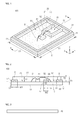
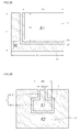
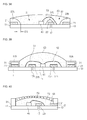
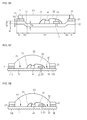
- Fig. 2 is a side sectional view taken along line A-A of Fig. 1 .
- Figs. 11 and 12 are side sectional views of a light emitting device according to second and third embodiments.
- Each of the metal layers 11 and 13 may have a thickness of about 15 ⁇ m to about 300 ⁇ m, and preferably, about 15 ⁇ m to about 50 ⁇ m. Also, the metal layers 11 and 13 may serve as a support frame for supporting the entire light emitting device and a heat-dissipating member for conducting heat generated from the light emitting chip 41. In outer areas of the metal layers 11 and 13, a length Y1 of a first direction Y and a length X1 of a second direction X perpendicular to the first direction Y may vary according to a size of the light emitting device 100.
- each of the insulation films 21 and 23 may include a light-transmitting or non-light-transmitting film.
- each of the insulation films 21 and 23 may include a polyimide (PI) film, a polyethylene terephthalate (PET) film, an ethylene vinyl acetate (EVA) film, a polyethylene naphthalate (PEN) film, a triacetyl cellulose (TAC) film, a polyamide imide (PAI) film, a polyether ether ketone (PEEK) film, a perfluoroalkoxy (PFA) film, a polyphenylene sulfide (PPS) film, and resin films (PE, PP, and PET).
- PI polyimide
- PET polyethylene terephthalate
- EVA ethylene vinyl acetate
- PEN polyethylene naphthalate
- TAC triacetyl cellulose
- PAI polyamide imide
- PEEK polyether ether ketone
- PFA perfluor
- Each of the insulation films 21 and 23 may be formed of a material having a predetermined reflective index, e.g., a reflective index of about 30% or more.
- the reflection characteristics of the insulation films 21 and 23 may improve surface reflection efficiency within the light emitting device 100.
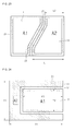
- One of the plurality of opened areas A1 and A2, e.g., the second opened area S2 may have a minimum width of about 60 ⁇ m.
- the bonding of a second wire 52 may be interrupted.
- the second opened area A2 may have a width of at least 60 ⁇ m.
- the first opened area A1 may have a width enough to mount the light emitting chip 41.
- the first opened area A1 may have a width wider than that of the second opened area A2.
- the first opened area A1 is described as an area on which the light emitting chip 41 is mounted and the second opened area A2 is described as an area to which a second wire 52 is bonded, the present disclosure is not limited thereto.
- the first opened area A1 may be an area to which a second wire 52 is bonded and the second opened area A2 may be an area on which the light emitting chip 41 is mounted.
- the first insulation film 21 may have a constant width W1. Alternatively, the first insulation film 21 may have widths different from each other. The first insulation film 21 may have a width W1 of several ten ⁇ m or more.
- the second insulation film 23 may have a constant width W2. Alternatively, the first insulation film 23 may have widths different from each other. The second insulation film 23 may have a width W2 greater than an interval G1 between the metal layers 11 and 13. For example, the second insulation film 23 may have a width of about 20 ⁇ m or more. The width W1 of the first insulation film 21 may be equal to or different from the W2 of the second insulation film 23.
- the second opened area A2 may have a minimum width of about 60 ⁇ m.
- the second opened area A2 may have a width at which a bonding process of a wire is not interrupted.
- the first opened area A1 may have a width enough to mount a light emitting chip.
- the first opened area A1 may have a width wider than that of the second opened area A2.
- the first opened area A1 is described as an area on which the light emitting chip is mounted and the second opened area A2 is described as an area to which the wire is bonded, the present disclosure is not limited thereto.
- the first opened area A1 may be an area to which the wire is bonded and the second opened area A2 may be an area on which the light emitting chip is mounted.
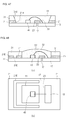
- Fig. 11 is a side sectional view of a light emitting device according to a second embodiment.
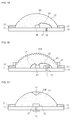
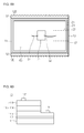
- a resin layer 61 is disposed on the first metal layer 11 and the second metal layer 13.
- the resin layer 61 may be injection-molded in a predetermined shape through a transfer molding method. According to the transfer molding method, a liquid resin is filled into a frame having a predetermined shape and then cured so that the resin layer 61 having a desired shape may be formed.
- the resin layer 61 may have a cylindrical shape, a polygonal column shape, or uneven surface shape, but is not limited thereto.
- An outer surface of the resin layer 61 may be spaced a predetermined interval T3 inward from an outer part of the first metal layer 11 or the second metal layer 13. Accordingly, the outer top surfaces of the first metal layer 11 and the second metal layer 13 may be exposed.
- the interval T3 may be about 1 ⁇ m or more.
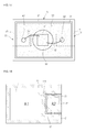
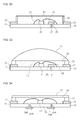
- the resin layer 63 is disposed on top surfaces of the metal layers 11 and 13.
- An insulation film 21 is disposed around the resin layer 63.
- the resin layer 63 may have a convex lens shape.
- a guide member 31 or a reflective material may be further disposed around the resin layer 63, but is not limited thereto.
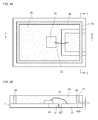
- a spacer 18 is disposed on a separation part 17 between the first metal layer 11 and the second metal layer 13.
- the spacer 18 is disposed between the first metal layer 11 and the second metal layer 13 and is formed of an insulation material.
- the spacer 18 adheres between the first metal layer 11 and the second metal layer 13.
- the spacer 18 may space the first metal layer 11 from the second metal layer 13 to prevent the first and second metal layers 11 and 13 from being electrically short-circuited with each other.
- the spacer 18 may be formed of at least one of SiO 2 , SiO x , SiO x N y , Si 3 N 4 , Al 2 O 3 , and TiO 2 .
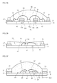
- the resin layer 63 may have a convex hemispherical shape. Also, a concave part 63B having a predetermined depth is defined in a center of the resin layer 63.
- the concave part 63B may have a horn shape or a hemispherical shape.
- a reflective material 72 may be disposed within the concave part 63B.
- the reflective material 72 may include a metal oxide.
- the reflective material 72 may form at least one layer formed of a material such as TiO 2 or/and SiO 2 to reflect incident light into a side direction.
- the resin layer 63 and the reflective material 72 may have refractive indexes different from each other.
- the reflective material 72 may have a refractive index greater than that of the resin layer 63.
- the resin layer 63 may reflect light of a center direction toward the side direction to uniformly provide orientation angle distribution of the light.
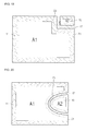
- the second guide member 37C may be disposed on top and inner surfaces of the second insulation film 23 to contact the top surface of the first metal layer 11.
- the second guide member 37B may be connected to the first guide member 37A and may be separated from the third guide member 37C.
- the second guide member 37C may be physically spaced from the second metal layer 13.
- the first to third guide members 37A, 37C, and 37B may be formed of the same material as or materials different from each other, but is not limited thereto.
- the first to third guide members 37A, 37C, and 37B may be formed of a metal material or an insulation material as another example.
- the first light emitting chip 41A may be electrically connected to the first metal layer 12A and the second metal layer 12B through a first wire 51A and a second wire 51B, respectively.
- the second light emitting chip 41B may be electrically connected to the second metal layer 12B and the third metal layer 12C through a third wire 51C and a fourth wire 51D, respectively.
- the first insulation film 21 may be disposed on the outer part B1 of the metal layers 11 and 13.
- the guide member 31 may be disposed on the firs insulation film 21.
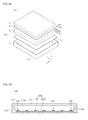
- the bottom cover 1011 may be formed of a metal material or a resin material. Also, the bottom cover 1011 may be manufactured using a press molding process or an extrusion molding process. The bottom cover 1011 may be formed of a metal or non-metal material having superior heat conductivity, but is not limited thereto.
- the substrate 1120 and the light emitting device 100 may be defined as a light emitting module 1060.
- the bottom cover 1152, at least one light emitting module 1060, the optical member 1154 may be defined as the light unit.
Landscapes
- Led Device Packages (AREA)
- Planar Illumination Modules (AREA)
- Non-Portable Lighting Devices Or Systems Thereof (AREA)
- Fastening Of Light Sources Or Lamp Holders (AREA)
Applications Claiming Priority (4)
| Application Number | Priority Date | Filing Date | Title |
|---|---|---|---|
| KR1020100076422 | 2010-08-09 | ||
| KR1020100076425A KR101154656B1 (ko) | 2010-08-09 | 2010-08-09 | 발광 소자 및 이를 구비한 조명 시스템 |
| KR1020100076423A KR101114151B1 (ko) | 2010-08-09 | 2010-08-09 | 발광 소자 및 이를 구비한 조명 시스템 |
| KR1020100076462A KR101172177B1 (ko) | 2010-08-09 | 2010-08-09 | 발광 소자 및 이를 구비한 조명 시스템 |
Publications (3)
| Publication Number | Publication Date |
|---|---|
| EP2418700A2 true EP2418700A2 (fr) | 2012-02-15 |
| EP2418700A3 EP2418700A3 (fr) | 2012-09-19 |
| EP2418700B1 EP2418700B1 (fr) | 2017-11-01 |
Family
ID=44381718
Family Applications (1)
| Application Number | Title | Priority Date | Filing Date |
|---|---|---|---|
| EP11176899.0A Not-in-force EP2418700B1 (fr) | 2010-08-09 | 2011-08-09 | Dispositif électroluminescent |
Country Status (5)
| Country | Link |
|---|---|
| US (2) | US8519426B2 (fr) |
| EP (1) | EP2418700B1 (fr) |
| JP (2) | JP5676395B2 (fr) |
| CN (1) | CN102376855B (fr) |
| TW (1) | TWI533483B (fr) |
Cited By (6)
| Publication number | Priority date | Publication date | Assignee | Title |
|---|---|---|---|---|
| EP2418701A3 (fr) * | 2010-08-09 | 2012-09-05 | LG Innotek Co., Ltd. | Dispositif électroluminescent et système d'éclairage |
| DE102013202551A1 (de) | 2013-02-18 | 2014-08-21 | Heraeus Materials Technologies GmbH & Co. KG | Verfahren zur Herstellung eines Substrats mit einer Kavität |
| DE102013202542A1 (de) | 2013-02-18 | 2014-09-18 | Heraeus Materials Technology Gmbh & Co. Kg | Substrat zur Herstellung einer LED und Verfahren zu dessen Herstellung |
| WO2015040107A1 (fr) * | 2013-09-23 | 2015-03-26 | Osram Opto Semiconductors Gmbh | Composant optoélectronique et procédé de fabrication de celui-ci |
| CN105591007A (zh) * | 2014-10-23 | 2016-05-18 | 展晶科技(深圳)有限公司 | 发光二极管封装结构 |
| DE102020133755A1 (de) | 2020-12-16 | 2022-06-23 | OSRAM Opto Semiconductors Gesellschaft mit beschränkter Haftung | Bauelement mit strukturiertem leiterrahmen und verfahren zur herstellung eines bauelements |
Families Citing this family (53)
| Publication number | Priority date | Publication date | Assignee | Title |
|---|---|---|---|---|
| US8878221B2 (en) | 2011-08-19 | 2014-11-04 | Lg Innotex Co., Ltd. | Light emitting module |
| KR20130096094A (ko) * | 2012-02-21 | 2013-08-29 | 엘지이노텍 주식회사 | 발광소자 패키지, 발광 소자 패키지 제조방법 및 이를 구비한 조명 시스템 |
| JP2013206895A (ja) * | 2012-03-27 | 2013-10-07 | Shin Etsu Chem Co Ltd | 光学半導体装置用基板とその製造方法、及び光学半導体装置とその製造方法 |
| KR20130115840A (ko) * | 2012-04-13 | 2013-10-22 | 이광희 | 모바일용 홍채인식 카메라시스템 |
| CN103489984B (zh) * | 2012-06-13 | 2017-09-12 | 亿光电子工业股份有限公司 | 发光二极管封装结构及其制作方法 |
| TWI500185B (zh) * | 2012-06-13 | 2015-09-11 | 億光電子工業股份有限公司 | 發光二極體封裝結構及其製作方法 |
| TW201403789A (zh) * | 2012-07-06 | 2014-01-16 | 隆達電子股份有限公司 | 發光二極體陣列 |
| US8927345B2 (en) * | 2012-07-09 | 2015-01-06 | Freescale Semiconductor, Inc. | Device package with rigid interconnect structure connecting die and substrate and method thereof |
| JP5995579B2 (ja) * | 2012-07-24 | 2016-09-21 | シチズンホールディングス株式会社 | 半導体発光装置及びその製造方法 |
| US8816507B2 (en) | 2012-07-26 | 2014-08-26 | Taiwan Semiconductor Manufacturing Company, Ltd. | Package-on-Package structures having buffer dams and method for forming the same |
| JP6093127B2 (ja) * | 2012-08-29 | 2017-03-08 | シャープ株式会社 | 発光装置及びその製造方法 |
| USD753612S1 (en) * | 2012-09-07 | 2016-04-12 | Cree, Inc. | Light emitter device |
| CN103682019B (zh) * | 2012-09-21 | 2017-04-19 | 展晶科技(深圳)有限公司 | 发光二极管及其制造方法 |
| CN103682018B (zh) * | 2012-09-21 | 2017-04-26 | 展晶科技(深圳)有限公司 | 发光二极管及其制造方法 |
| JP2014085653A (ja) * | 2012-10-26 | 2014-05-12 | Funai Electric Co Ltd | 表示装置 |
| DE102012110774A1 (de) | 2012-11-09 | 2014-05-15 | Osram Opto Semiconductors Gmbh | Optoelektronisches Halbleiterbauteil |
| CN103887402B (zh) * | 2012-12-21 | 2018-02-09 | 光宝电子(广州)有限公司 | 发光二极管封装结构、其围墙结构及围墙结构的制造方法 |
| US9029905B2 (en) * | 2012-12-21 | 2015-05-12 | Lite-On Opto Technology (Changzhou) Co., Ltd. | Light emitting diode device |
| CN103972355A (zh) * | 2013-01-29 | 2014-08-06 | 台达电子工业股份有限公司 | 发光元件及其制作方法 |
| DE102013207564A1 (de) * | 2013-04-25 | 2014-10-30 | Osram Opto Semiconductors Gmbh | Wellenlängenkonvertierendes Element, optoelektronisches Bauelement und Druckschablone |
| KR102056832B1 (ko) * | 2013-05-31 | 2019-12-17 | 엘지이노텍 주식회사 | 인쇄회로기판 및 그 인쇄회로기판을 포함하는 조명 유닛 |
| CN105359284B (zh) * | 2013-06-28 | 2019-05-14 | 西铁城时计株式会社 | Led装置 |
| KR102080778B1 (ko) * | 2013-09-11 | 2020-04-14 | 엘지이노텍 주식회사 | 발광 소자 패키지 |
| DE102013225552A1 (de) * | 2013-12-11 | 2015-06-11 | Osram Opto Semiconductors Gmbh | Optoelektronisches Bauelement |
| DE102014101556A1 (de) | 2014-02-07 | 2015-08-13 | Osram Opto Semiconductors Gmbh | Optoelektronisches Bauelement und Verfahren zu seiner Herstellung |
| TWI557955B (zh) * | 2014-04-23 | 2016-11-11 | 光寶光電(常州)有限公司 | Led承載座及其製造方法 |
| DE102014108282A1 (de) * | 2014-06-12 | 2015-12-17 | Osram Opto Semiconductors Gmbh | Optoelektronisches Halbleiterbauelement, Verfahren zur Herstellung eines optoelektronischen Halbleiterbauelements sowie Lichtquelle mit einem optoelektronischen Halbleiterbauelement |
| US9423247B2 (en) * | 2014-06-18 | 2016-08-23 | Shenzhen China Star Optoelectronics Technology Co., Ltd. | Positioning graphic component for substrate detection and method of manufacturing the same |
| KR102237112B1 (ko) * | 2014-07-30 | 2021-04-08 | 엘지이노텍 주식회사 | 발광 소자 및 이를 구비한 광원 모듈 |
| DE102014115375A1 (de) * | 2014-08-08 | 2016-02-11 | Epcos Ag | Träger für eine LED |
| JP6583764B2 (ja) * | 2014-09-12 | 2019-10-02 | パナソニックIpマネジメント株式会社 | 発光装置、及び照明装置 |
| TW201628218A (zh) * | 2015-01-26 | 2016-08-01 | 艾笛森光電股份有限公司 | 磷光片與具有磷光片的發光裝置 |
| EP3091822A1 (fr) * | 2015-05-08 | 2016-11-09 | AT & S Austria Technologie & Systemtechnik Aktiengesellschaft | Procédé pour la production d'un module électronique ainsi que module électronique correspondant |
| KR102378761B1 (ko) * | 2015-07-21 | 2022-03-25 | 엘지이노텍 주식회사 | 일체형 발광 패키지 및 이를 이용한 차량용 램프 |
| JP6406711B2 (ja) * | 2015-10-28 | 2018-10-17 | 大口マテリアル株式会社 | リードフレームの製造方法 |
| US10326066B2 (en) * | 2015-10-29 | 2019-06-18 | Kyocera Corporation | Light emitting element-mounting substrate and light emitting apparatus |
| DE112015007119B4 (de) | 2015-11-12 | 2026-04-02 | OSRAM Opto Semiconductors Gesellschaft mit beschränkter Haftung | Package für eine elektronische Komponente, elektronische Komponente und elektronische Anordnung |
| JP6118437B1 (ja) * | 2015-12-21 | 2017-04-19 | ルーメンス カンパニー リミテッド | Ledモジュール |
| US10211378B2 (en) | 2016-01-29 | 2019-02-19 | Nichia Corporation | Light emitting device and method for manufacturing same |
| JP6952945B2 (ja) * | 2016-03-25 | 2021-10-27 | スージョウ レキン セミコンダクター カンパニー リミテッド | 発光素子パッケージ及び照明装置 |
| JP2017188597A (ja) * | 2016-04-07 | 2017-10-12 | アズビル株式会社 | 基板ユニットおよび基板ユニットの製造方法 |
| JP6873157B2 (ja) | 2016-05-02 | 2021-05-19 | ルミレッズ ホールディング ベーフェー | 熱ブロックアセンブリ、それを有するled装置、及び熱ブロックアセンブリを製造する方法 |
| FR3051033B1 (fr) * | 2016-05-05 | 2020-08-28 | Linxens Holding | Dispositif emetteur de lumiere |
| JPWO2017209143A1 (ja) * | 2016-05-31 | 2019-03-28 | シチズン電子株式会社 | 発光装置およびその製造方法 |
| US10910540B2 (en) * | 2017-04-04 | 2021-02-02 | Signify Holding B.V. | Solid state light emitter die having a heat spreader between a plurality lead frame |
| JP7177327B2 (ja) * | 2017-04-06 | 2022-11-24 | 日亜化学工業株式会社 | 発光装置 |
| CN110959199B (zh) * | 2017-08-28 | 2023-12-15 | 奥斯兰姆奥普托半导体有限责任公司 | 光电子半导体器件和用于形成光电子半导体器件的方法 |
| TWI677976B (zh) * | 2018-06-29 | 2019-11-21 | 相豐科技股份有限公司 | 發光顯像單元的複合層結構 |
| CN111665640B (zh) * | 2019-03-08 | 2022-07-26 | 三赢科技(深圳)有限公司 | 结构光投射模组及其电子装置 |
| JP7417031B2 (ja) * | 2019-03-27 | 2024-01-18 | 日亜化学工業株式会社 | 発光装置 |
| JP7117684B2 (ja) * | 2020-01-31 | 2022-08-15 | 日亜化学工業株式会社 | 面状光源の製造方法 |
| TWI719823B (zh) * | 2020-02-05 | 2021-02-21 | 聚積科技股份有限公司 | 板上封裝顯示元件及其製造方法 |
| JP7494521B2 (ja) * | 2020-03-30 | 2024-06-04 | 富士電機株式会社 | 半導体装置及び半導体装置の製造方法 |
Family Cites Families (57)
| Publication number | Priority date | Publication date | Assignee | Title |
|---|---|---|---|---|
| JPS6359356A (ja) * | 1986-08-28 | 1988-03-15 | 株式会社 山本製作所 | 竪型衝撃式脱ふ装置 |
| FR2645680B1 (fr) * | 1989-04-07 | 1994-04-29 | Thomson Microelectronics Sa Sg | Encapsulation de modules electroniques et procede de fabrication |
| JPH0796634A (ja) | 1993-06-24 | 1995-04-11 | Ricoh Co Ltd | Led書き込み装置および画像形成装置 |
| JP3020787B2 (ja) | 1993-12-20 | 2000-03-15 | 京セラ株式会社 | 画像装置 |
| US6680569B2 (en) * | 1999-02-18 | 2004-01-20 | Lumileds Lighting U.S. Llc | Red-deficiency compensating phosphor light emitting device |
| KR100354823B1 (ko) | 1999-09-10 | 2002-10-04 | 전자부품연구원 | 투명 절연층을 이용한 후막형 전계 발광 소자 |
| MY145695A (en) * | 2001-01-24 | 2012-03-30 | Nichia Corp | Light emitting diode, optical semiconductor device, epoxy resin composition suited for optical semiconductor device, and method for manufacturing the same |
| JP3939177B2 (ja) * | 2002-03-20 | 2007-07-04 | シャープ株式会社 | 発光装置の製造方法 |
| TW546799B (en) * | 2002-06-26 | 2003-08-11 | Lingsen Precision Ind Ltd | Packaged formation method of LED and product structure |
| DE10228634A1 (de) * | 2002-06-26 | 2004-01-22 | Osram Opto Semiconductors Gmbh | Oberflächenmontierbare Miniatur-Lumineszenz-und/oder Photo-Diode und Verfahren zu deren Herstellung |
| CN100533723C (zh) | 2002-08-05 | 2009-08-26 | 奥斯兰姆奥普托半导体有限责任公司 | 电引线架的制造方法,表面安装的半导体器件的制造方法和引线架带 |
| JP4633333B2 (ja) * | 2003-01-23 | 2011-02-16 | 株式会社光波 | 発光装置 |
| JP3910171B2 (ja) * | 2003-02-18 | 2007-04-25 | シャープ株式会社 | 半導体発光装置、その製造方法および電子撮像装置 |
| JP4034241B2 (ja) * | 2003-06-27 | 2008-01-16 | 日本ライツ株式会社 | 光源装置および光源装置の製造方法 |
| US7082640B2 (en) | 2003-07-18 | 2006-08-01 | Christy, Inc. | Ambient air backflushed filter vacuum |
| KR100533635B1 (ko) * | 2003-11-20 | 2005-12-06 | 삼성전기주식회사 | Led 패키지 |
| US20050116235A1 (en) * | 2003-12-02 | 2005-06-02 | Schultz John C. | Illumination assembly |
| KR100623024B1 (ko) * | 2004-06-10 | 2006-09-19 | 엘지전자 주식회사 | 고출력 led 패키지 |
| US7473933B2 (en) * | 2004-10-29 | 2009-01-06 | Ledengin, Inc. (Cayman) | High power LED package with universal bonding pads and interconnect arrangement |
| JP5262374B2 (ja) * | 2004-11-30 | 2013-08-14 | 日亜化学工業株式会社 | 樹脂成形体及び表面実装型発光装置並びにそれらの製造方法 |
| US20060125716A1 (en) * | 2004-12-10 | 2006-06-15 | Wong Lye Y | Light-emitting diode display with compartment |
| JP2006186000A (ja) * | 2004-12-27 | 2006-07-13 | Kyoei Opto Japan Kk | 高出力半導体装置及びその製造方法 |
| JP2006303458A (ja) * | 2005-03-25 | 2006-11-02 | Naoya Yanase | 電子部品実装基板 |
| TWI256737B (en) * | 2005-05-19 | 2006-06-11 | Pi-Fu Yang | One-block light-emitting device and manufacturing method thereof |
| KR100665219B1 (ko) | 2005-07-14 | 2007-01-09 | 삼성전기주식회사 | 파장변환형 발광다이오드 패키지 |
| DE102005041064B4 (de) * | 2005-08-30 | 2023-01-19 | OSRAM Opto Semiconductors Gesellschaft mit beschränkter Haftung | Oberflächenmontierbares optoelektronisches Bauelement und Verfahren zu dessen Herstellung |
| KR100691441B1 (ko) | 2005-11-15 | 2007-03-09 | 삼성전기주식회사 | 발광 다이오드 패키지 |
| US20070126020A1 (en) * | 2005-12-03 | 2007-06-07 | Cheng Lin | High-power LED chip packaging structure and fabrication method thereof |
| JP2007194517A (ja) | 2006-01-23 | 2007-08-02 | Matsushita Electric Ind Co Ltd | 発光モジュールとその製造方法 |
| JP4931628B2 (ja) * | 2006-03-09 | 2012-05-16 | セイコーインスツル株式会社 | 照明装置及びこれを備える表示装置 |
| WO2007135707A1 (fr) * | 2006-05-18 | 2007-11-29 | Nichia Corporation | Corps moulé en résine et dispositif électroluminescent monté en surface, procédé de fabrication correspondant |
| KR20080028071A (ko) | 2006-09-26 | 2008-03-31 | 서울옵토디바이스주식회사 | 후방에 광 반사패턴을 갖는 led 장치 |
| JP2008108835A (ja) * | 2006-10-24 | 2008-05-08 | Harison Toshiba Lighting Corp | 半導体発光装置及びその製造方法 |
| KR100764449B1 (ko) | 2006-10-24 | 2007-10-05 | 삼성전기주식회사 | 발광소자 패키지 |
| TWM318795U (en) | 2006-12-18 | 2007-09-11 | Lighthouse Technology Co Ltd | Package structure |
| JP5168152B2 (ja) | 2006-12-28 | 2013-03-21 | 日亜化学工業株式会社 | 発光装置 |
| JP2008198782A (ja) | 2007-02-13 | 2008-08-28 | Toyoda Gosei Co Ltd | 発光装置 |
| JP2008226928A (ja) * | 2007-03-08 | 2008-09-25 | Sharp Corp | 発光装置およびその製造方法、ならびに照明装置 |
| JP4205135B2 (ja) * | 2007-03-13 | 2009-01-07 | シャープ株式会社 | 半導体発光装置、半導体発光装置用多連リードフレーム |
| KR100850666B1 (ko) * | 2007-03-30 | 2008-08-07 | 서울반도체 주식회사 | 메탈 pcb를 갖는 led 패키지 |
| KR200442383Y1 (ko) | 2007-07-18 | 2008-11-05 | 주식회사 파워라이텍 | 발광다이오드 소자의 어셈블리 구조 |
| JP5062677B2 (ja) * | 2007-09-18 | 2012-10-31 | 株式会社ジャパンディスプレイウェスト | 表示装置 |
| KR20090039261A (ko) | 2007-10-18 | 2009-04-22 | 삼성전기주식회사 | 발광다이오드 패키지 |
| KR101423723B1 (ko) | 2007-10-29 | 2014-08-04 | 서울바이오시스 주식회사 | 발광 다이오드 패키지 |
| TW200937667A (en) * | 2008-02-20 | 2009-09-01 | Advanced Optoelectronic Tech | Package structure of chemical compound semiconductor device and fabricating method thereof |
| US8258526B2 (en) | 2008-07-03 | 2012-09-04 | Samsung Led Co., Ltd. | Light emitting diode package including a lead frame with a cavity |
| KR20100028136A (ko) | 2008-08-21 | 2010-03-12 | 삼성전기주식회사 | Led 패키지 모듈 |
| KR100982994B1 (ko) * | 2008-10-15 | 2010-09-17 | 삼성엘이디 주식회사 | Led 패키지 모듈 |
| JP2010109119A (ja) * | 2008-10-30 | 2010-05-13 | Sanyo Electric Co Ltd | 発光モジュール及びその製造方法 |
| JP2010114387A (ja) * | 2008-11-10 | 2010-05-20 | Sanyo Electric Co Ltd | 発光装置及びその製造方法、並びに、発光モジュール |
| KR20100052978A (ko) | 2008-11-11 | 2010-05-20 | 주식회사 동부하이텍 | 조명 장치 및 그 구동방법 |
| JP2010118528A (ja) * | 2008-11-13 | 2010-05-27 | Sumitomo Metal Electronics Devices Inc | リフレクタ及びこれを用いる発光素子搭載用パッケージ |
| KR101018153B1 (ko) * | 2008-11-27 | 2011-02-28 | 삼성엘이디 주식회사 | Led 패키지 |
| KR101161408B1 (ko) | 2009-03-05 | 2012-07-02 | 삼성엘이디 주식회사 | 발광 다이오드 패키지 및 그의 제조 방법 |
| KR20100135496A (ko) | 2009-06-17 | 2010-12-27 | 산요덴키가부시키가이샤 | 발광 장치 및 그 제조 방법 |
| JP3158994U (ja) | 2009-10-29 | 2010-05-06 | 株式会社Ks | 回路基板 |
| KR101114197B1 (ko) | 2010-08-09 | 2012-02-22 | 엘지이노텍 주식회사 | 발광 소자 및 이를 구비한 조명 시스템 |
-
2011
- 2011-08-09 TW TW100128371A patent/TWI533483B/zh not_active IP Right Cessation
- 2011-08-09 EP EP11176899.0A patent/EP2418700B1/fr not_active Not-in-force
- 2011-08-09 US US13/206,229 patent/US8519426B2/en not_active Expired - Fee Related
- 2011-08-09 CN CN201110228866.4A patent/CN102376855B/zh not_active Expired - Fee Related
- 2011-08-09 JP JP2011174180A patent/JP5676395B2/ja not_active Expired - Fee Related
-
2013
- 2013-08-16 US US13/969,296 patent/US9041013B2/en active Active
-
2014
- 2014-09-05 JP JP2014181513A patent/JP5869080B2/ja not_active Expired - Fee Related
Non-Patent Citations (1)
| Title |
|---|
| None |
Cited By (11)
| Publication number | Priority date | Publication date | Assignee | Title |
|---|---|---|---|---|
| EP2418701A3 (fr) * | 2010-08-09 | 2012-09-05 | LG Innotek Co., Ltd. | Dispositif électroluminescent et système d'éclairage |
| US8519427B2 (en) | 2010-08-09 | 2013-08-27 | Lg Innotek Co., Ltd. | Light emitting device and lighting system |
| DE102013202551A1 (de) | 2013-02-18 | 2014-08-21 | Heraeus Materials Technologies GmbH & Co. KG | Verfahren zur Herstellung eines Substrats mit einer Kavität |
| DE102013202542A1 (de) | 2013-02-18 | 2014-09-18 | Heraeus Materials Technology Gmbh & Co. Kg | Substrat zur Herstellung einer LED und Verfahren zu dessen Herstellung |
| WO2015040107A1 (fr) * | 2013-09-23 | 2015-03-26 | Osram Opto Semiconductors Gmbh | Composant optoélectronique et procédé de fabrication de celui-ci |
| US9853198B2 (en) | 2013-09-23 | 2017-12-26 | Osram Opto Semiconductors Gmbh | Optoelectronic component and method of producing same |
| CN105591007A (zh) * | 2014-10-23 | 2016-05-18 | 展晶科技(深圳)有限公司 | 发光二极管封装结构 |
| TWI550914B (zh) * | 2014-10-23 | 2016-09-21 | 榮創能源科技股份有限公司 | 發光二極體封裝結構 |
| US9640742B2 (en) | 2014-10-23 | 2017-05-02 | Advanced Optoelectronic Technology, Inc. | LED package with reflecting cup |
| CN105591007B (zh) * | 2014-10-23 | 2018-04-03 | 展晶科技(深圳)有限公司 | 发光二极管封装结构 |
| DE102020133755A1 (de) | 2020-12-16 | 2022-06-23 | OSRAM Opto Semiconductors Gesellschaft mit beschränkter Haftung | Bauelement mit strukturiertem leiterrahmen und verfahren zur herstellung eines bauelements |
Also Published As
| Publication number | Publication date |
|---|---|
| US20110309404A1 (en) | 2011-12-22 |
| JP2012039121A (ja) | 2012-02-23 |
| JP5676395B2 (ja) | 2015-02-25 |
| US8519426B2 (en) | 2013-08-27 |
| EP2418700B1 (fr) | 2017-11-01 |
| JP5869080B2 (ja) | 2016-02-24 |
| CN102376855B (zh) | 2015-08-19 |
| TWI533483B (zh) | 2016-05-11 |
| EP2418700A3 (fr) | 2012-09-19 |
| TW201216534A (en) | 2012-04-16 |
| JP2014241444A (ja) | 2014-12-25 |
| US20130328094A1 (en) | 2013-12-12 |
| CN102376855A (zh) | 2012-03-14 |
| US9041013B2 (en) | 2015-05-26 |
Similar Documents
| Publication | Publication Date | Title |
|---|---|---|
| EP2418700B1 (fr) | Dispositif électroluminescent | |
| US8519427B2 (en) | Light emitting device and lighting system | |
| US8399904B2 (en) | Light emitting device and lighting system having the same | |
| KR101163901B1 (ko) | 발광 소자 및 이를 구비한 조명 시스템 | |
| KR101154671B1 (ko) | 발광 소자 및 이를 구비한 조명 시스템 | |
| KR101125437B1 (ko) | 발광 소자 및 이를 구비한 조명 시스템 | |
| KR101114151B1 (ko) | 발광 소자 및 이를 구비한 조명 시스템 | |
| KR101154656B1 (ko) | 발광 소자 및 이를 구비한 조명 시스템 | |
| KR101172177B1 (ko) | 발광 소자 및 이를 구비한 조명 시스템 | |
| KR101114094B1 (ko) | 발광 소자 및 이를 구비한 조명 시스템 | |
| KR101189329B1 (ko) | 발광 소자 및 이를 구비한 조명 시스템 |
Legal Events
| Date | Code | Title | Description |
|---|---|---|---|
| 17P | Request for examination filed |
Effective date: 20110809 |
|
| AK | Designated contracting states |
Kind code of ref document: A2 Designated state(s): AL AT BE BG CH CY CZ DE DK EE ES FI FR GB GR HR HU IE IS IT LI LT LU LV MC MK MT NL NO PL PT RO RS SE SI SK SM TR |
|
| AX | Request for extension of the european patent |
Extension state: BA ME |
|
| PUAI | Public reference made under article 153(3) epc to a published international application that has entered the european phase |
Free format text: ORIGINAL CODE: 0009012 |
|
| RIC1 | Information provided on ipc code assigned before grant |
Ipc: H01L 33/48 20100101AFI20120426BHEP Ipc: H01L 33/50 20100101ALN20120426BHEP Ipc: H01L 33/62 20100101ALN20120426BHEP Ipc: H01L 33/64 20100101ALN20120426BHEP Ipc: H01L 33/60 20100101ALN20120426BHEP |
|
| PUAL | Search report despatched |
Free format text: ORIGINAL CODE: 0009013 |
|
| AK | Designated contracting states |
Kind code of ref document: A3 Designated state(s): AL AT BE BG CH CY CZ DE DK EE ES FI FR GB GR HR HU IE IS IT LI LT LU LV MC MK MT NL NO PL PT RO RS SE SI SK SM TR |
|
| AX | Request for extension of the european patent |
Extension state: BA ME |
|
| RIC1 | Information provided on ipc code assigned before grant |
Ipc: H01L 33/62 20100101ALN20120815BHEP Ipc: H01L 33/48 20100101AFI20120815BHEP Ipc: H01L 33/60 20100101ALN20120815BHEP Ipc: H01L 33/64 20100101ALN20120815BHEP Ipc: H01L 33/50 20100101ALN20120815BHEP |
|
| RIC1 | Information provided on ipc code assigned before grant |
Ipc: H01L 33/60 20100101ALN20120822BHEP Ipc: H01L 33/64 20100101ALN20120822BHEP Ipc: H01L 33/62 20100101ALN20120822BHEP Ipc: H01L 33/50 20100101ALN20120822BHEP Ipc: H01L 33/48 20100101AFI20120822BHEP |
|
| RIC1 | Information provided on ipc code assigned before grant |
Ipc: H01L 33/64 20100101ALN20120828BHEP Ipc: H01L 33/50 20100101ALN20120828BHEP Ipc: H01L 33/60 20100101ALN20120828BHEP Ipc: H01L 33/62 20100101ALN20120828BHEP Ipc: H01L 33/48 20100101AFI20120828BHEP |
|
| 17Q | First examination report despatched |
Effective date: 20150903 |
|
| RAP1 | Party data changed (applicant data changed or rights of an application transferred) |
Owner name: LG INNOTEK CO., LTD. |
|
| GRAP | Despatch of communication of intention to grant a patent |
Free format text: ORIGINAL CODE: EPIDOSNIGR1 |
|
| INTG | Intention to grant announced |
Effective date: 20170523 |
|
| GRAS | Grant fee paid |
Free format text: ORIGINAL CODE: EPIDOSNIGR3 |
|
| GRAA | (expected) grant |
Free format text: ORIGINAL CODE: 0009210 |
|
| AK | Designated contracting states |
Kind code of ref document: B1 Designated state(s): AL AT BE BG CH CY CZ DE DK EE ES FI FR GB GR HR HU IE IS IT LI LT LU LV MC MK MT NL NO PL PT RO RS SE SI SK SM TR |
|
| REG | Reference to a national code |
Ref country code: GB Ref legal event code: FG4D |
|
| REG | Reference to a national code |
Ref country code: CH Ref legal event code: EP Ref country code: AT Ref legal event code: REF Ref document number: 942841 Country of ref document: AT Kind code of ref document: T Effective date: 20171115 |
|
| REG | Reference to a national code |
Ref country code: IE Ref legal event code: FG4D |
|
| REG | Reference to a national code |
Ref country code: DE Ref legal event code: R096 Ref document number: 602011042850 Country of ref document: DE |
|
| REG | Reference to a national code |
Ref country code: NL Ref legal event code: MP Effective date: 20171101 |
|
| REG | Reference to a national code |
Ref country code: LT Ref legal event code: MG4D |
|
| REG | Reference to a national code |
Ref country code: AT Ref legal event code: MK05 Ref document number: 942841 Country of ref document: AT Kind code of ref document: T Effective date: 20171101 |
|
| PG25 | Lapsed in a contracting state [announced via postgrant information from national office to epo] |
Ref country code: NO Free format text: LAPSE BECAUSE OF FAILURE TO SUBMIT A TRANSLATION OF THE DESCRIPTION OR TO PAY THE FEE WITHIN THE PRESCRIBED TIME-LIMIT Effective date: 20180201 Ref country code: ES Free format text: LAPSE BECAUSE OF FAILURE TO SUBMIT A TRANSLATION OF THE DESCRIPTION OR TO PAY THE FEE WITHIN THE PRESCRIBED TIME-LIMIT Effective date: 20171101 Ref country code: LT Free format text: LAPSE BECAUSE OF FAILURE TO SUBMIT A TRANSLATION OF THE DESCRIPTION OR TO PAY THE FEE WITHIN THE PRESCRIBED TIME-LIMIT Effective date: 20171101 Ref country code: SE Free format text: LAPSE BECAUSE OF FAILURE TO SUBMIT A TRANSLATION OF THE DESCRIPTION OR TO PAY THE FEE WITHIN THE PRESCRIBED TIME-LIMIT Effective date: 20171101 Ref country code: NL Free format text: LAPSE BECAUSE OF FAILURE TO SUBMIT A TRANSLATION OF THE DESCRIPTION OR TO PAY THE FEE WITHIN THE PRESCRIBED TIME-LIMIT Effective date: 20171101 Ref country code: FI Free format text: LAPSE BECAUSE OF FAILURE TO SUBMIT A TRANSLATION OF THE DESCRIPTION OR TO PAY THE FEE WITHIN THE PRESCRIBED TIME-LIMIT Effective date: 20171101 |
|
| PG25 | Lapsed in a contracting state [announced via postgrant information from national office to epo] |
Ref country code: BG Free format text: LAPSE BECAUSE OF FAILURE TO SUBMIT A TRANSLATION OF THE DESCRIPTION OR TO PAY THE FEE WITHIN THE PRESCRIBED TIME-LIMIT Effective date: 20180201 Ref country code: HR Free format text: LAPSE BECAUSE OF FAILURE TO SUBMIT A TRANSLATION OF THE DESCRIPTION OR TO PAY THE FEE WITHIN THE PRESCRIBED TIME-LIMIT Effective date: 20171101 Ref country code: LV Free format text: LAPSE BECAUSE OF FAILURE TO SUBMIT A TRANSLATION OF THE DESCRIPTION OR TO PAY THE FEE WITHIN THE PRESCRIBED TIME-LIMIT Effective date: 20171101 Ref country code: RS Free format text: LAPSE BECAUSE OF FAILURE TO SUBMIT A TRANSLATION OF THE DESCRIPTION OR TO PAY THE FEE WITHIN THE PRESCRIBED TIME-LIMIT Effective date: 20171101 Ref country code: GR Free format text: LAPSE BECAUSE OF FAILURE TO SUBMIT A TRANSLATION OF THE DESCRIPTION OR TO PAY THE FEE WITHIN THE PRESCRIBED TIME-LIMIT Effective date: 20180202 Ref country code: IS Free format text: LAPSE BECAUSE OF FAILURE TO SUBMIT A TRANSLATION OF THE DESCRIPTION OR TO PAY THE FEE WITHIN THE PRESCRIBED TIME-LIMIT Effective date: 20180301 Ref country code: AT Free format text: LAPSE BECAUSE OF FAILURE TO SUBMIT A TRANSLATION OF THE DESCRIPTION OR TO PAY THE FEE WITHIN THE PRESCRIBED TIME-LIMIT Effective date: 20171101 |
|
| PG25 | Lapsed in a contracting state [announced via postgrant information from national office to epo] |
Ref country code: DK Free format text: LAPSE BECAUSE OF FAILURE TO SUBMIT A TRANSLATION OF THE DESCRIPTION OR TO PAY THE FEE WITHIN THE PRESCRIBED TIME-LIMIT Effective date: 20171101 Ref country code: SK Free format text: LAPSE BECAUSE OF FAILURE TO SUBMIT A TRANSLATION OF THE DESCRIPTION OR TO PAY THE FEE WITHIN THE PRESCRIBED TIME-LIMIT Effective date: 20171101 Ref country code: EE Free format text: LAPSE BECAUSE OF FAILURE TO SUBMIT A TRANSLATION OF THE DESCRIPTION OR TO PAY THE FEE WITHIN THE PRESCRIBED TIME-LIMIT Effective date: 20171101 Ref country code: CY Free format text: LAPSE BECAUSE OF FAILURE TO SUBMIT A TRANSLATION OF THE DESCRIPTION OR TO PAY THE FEE WITHIN THE PRESCRIBED TIME-LIMIT Effective date: 20171101 Ref country code: CZ Free format text: LAPSE BECAUSE OF FAILURE TO SUBMIT A TRANSLATION OF THE DESCRIPTION OR TO PAY THE FEE WITHIN THE PRESCRIBED TIME-LIMIT Effective date: 20171101 |
|
| REG | Reference to a national code |
Ref country code: DE Ref legal event code: R097 Ref document number: 602011042850 Country of ref document: DE |
|
| PG25 | Lapsed in a contracting state [announced via postgrant information from national office to epo] |
Ref country code: PL Free format text: LAPSE BECAUSE OF FAILURE TO SUBMIT A TRANSLATION OF THE DESCRIPTION OR TO PAY THE FEE WITHIN THE PRESCRIBED TIME-LIMIT Effective date: 20171101 Ref country code: SM Free format text: LAPSE BECAUSE OF FAILURE TO SUBMIT A TRANSLATION OF THE DESCRIPTION OR TO PAY THE FEE WITHIN THE PRESCRIBED TIME-LIMIT Effective date: 20171101 Ref country code: IT Free format text: LAPSE BECAUSE OF FAILURE TO SUBMIT A TRANSLATION OF THE DESCRIPTION OR TO PAY THE FEE WITHIN THE PRESCRIBED TIME-LIMIT Effective date: 20171101 Ref country code: RO Free format text: LAPSE BECAUSE OF FAILURE TO SUBMIT A TRANSLATION OF THE DESCRIPTION OR TO PAY THE FEE WITHIN THE PRESCRIBED TIME-LIMIT Effective date: 20171101 |
|
| PLBE | No opposition filed within time limit |
Free format text: ORIGINAL CODE: 0009261 |
|
| STAA | Information on the status of an ep patent application or granted ep patent |
Free format text: STATUS: NO OPPOSITION FILED WITHIN TIME LIMIT |
|
| 26N | No opposition filed |
Effective date: 20180802 |
|
| PG25 | Lapsed in a contracting state [announced via postgrant information from national office to epo] |
Ref country code: SI Free format text: LAPSE BECAUSE OF FAILURE TO SUBMIT A TRANSLATION OF THE DESCRIPTION OR TO PAY THE FEE WITHIN THE PRESCRIBED TIME-LIMIT Effective date: 20171101 |
|
| PG25 | Lapsed in a contracting state [announced via postgrant information from national office to epo] |
Ref country code: MC Free format text: LAPSE BECAUSE OF FAILURE TO SUBMIT A TRANSLATION OF THE DESCRIPTION OR TO PAY THE FEE WITHIN THE PRESCRIBED TIME-LIMIT Effective date: 20171101 |
|
| REG | Reference to a national code |
Ref country code: CH Ref legal event code: PL |
|
| GBPC | Gb: european patent ceased through non-payment of renewal fee |
Effective date: 20180809 |
|
| PG25 | Lapsed in a contracting state [announced via postgrant information from national office to epo] |
Ref country code: CH Free format text: LAPSE BECAUSE OF NON-PAYMENT OF DUE FEES Effective date: 20180831 Ref country code: LU Free format text: LAPSE BECAUSE OF NON-PAYMENT OF DUE FEES Effective date: 20180809 Ref country code: LI Free format text: LAPSE BECAUSE OF NON-PAYMENT OF DUE FEES Effective date: 20180831 |
|
| REG | Reference to a national code |
Ref country code: BE Ref legal event code: MM Effective date: 20180831 |
|
| REG | Reference to a national code |
Ref country code: IE Ref legal event code: MM4A |
|
| PG25 | Lapsed in a contracting state [announced via postgrant information from national office to epo] |
Ref country code: IE Free format text: LAPSE BECAUSE OF NON-PAYMENT OF DUE FEES Effective date: 20180809 |
|
| PG25 | Lapsed in a contracting state [announced via postgrant information from national office to epo] |
Ref country code: BE Free format text: LAPSE BECAUSE OF NON-PAYMENT OF DUE FEES Effective date: 20180831 Ref country code: FR Free format text: LAPSE BECAUSE OF NON-PAYMENT OF DUE FEES Effective date: 20180831 |
|
| PG25 | Lapsed in a contracting state [announced via postgrant information from national office to epo] |
Ref country code: GB Free format text: LAPSE BECAUSE OF NON-PAYMENT OF DUE FEES Effective date: 20180809 |
|
| PG25 | Lapsed in a contracting state [announced via postgrant information from national office to epo] |
Ref country code: MT Free format text: LAPSE BECAUSE OF NON-PAYMENT OF DUE FEES Effective date: 20180809 |
|
| PG25 | Lapsed in a contracting state [announced via postgrant information from national office to epo] |
Ref country code: TR Free format text: LAPSE BECAUSE OF FAILURE TO SUBMIT A TRANSLATION OF THE DESCRIPTION OR TO PAY THE FEE WITHIN THE PRESCRIBED TIME-LIMIT Effective date: 20171101 |
|
| PG25 | Lapsed in a contracting state [announced via postgrant information from national office to epo] |
Ref country code: HU Free format text: LAPSE BECAUSE OF FAILURE TO SUBMIT A TRANSLATION OF THE DESCRIPTION OR TO PAY THE FEE WITHIN THE PRESCRIBED TIME-LIMIT; INVALID AB INITIO Effective date: 20110809 Ref country code: PT Free format text: LAPSE BECAUSE OF FAILURE TO SUBMIT A TRANSLATION OF THE DESCRIPTION OR TO PAY THE FEE WITHIN THE PRESCRIBED TIME-LIMIT Effective date: 20171101 |
|
| PG25 | Lapsed in a contracting state [announced via postgrant information from national office to epo] |
Ref country code: MK Free format text: LAPSE BECAUSE OF NON-PAYMENT OF DUE FEES Effective date: 20171101 |
|
| PG25 | Lapsed in a contracting state [announced via postgrant information from national office to epo] |
Ref country code: AL Free format text: LAPSE BECAUSE OF FAILURE TO SUBMIT A TRANSLATION OF THE DESCRIPTION OR TO PAY THE FEE WITHIN THE PRESCRIBED TIME-LIMIT Effective date: 20171101 |
|
| REG | Reference to a national code |
Ref country code: DE Ref legal event code: R081 Ref document number: 602011042850 Country of ref document: DE Owner name: SUZHOU LEKIN SEMICONDUCTOR CO. LTD., TAICANG, CN Free format text: FORMER OWNER: LG INNOTEK CO., LTD., SEOUL, KR |
|
| PGFP | Annual fee paid to national office [announced via postgrant information from national office to epo] |
Ref country code: DE Payment date: 20230712 Year of fee payment: 13 |
|
| REG | Reference to a national code |
Ref country code: DE Ref legal event code: R079 Ref document number: 602011042850 Country of ref document: DE Free format text: PREVIOUS MAIN CLASS: H01L0033480000 Ipc: H10H0020850000 |
|
| REG | Reference to a national code |
Ref country code: DE Ref legal event code: R119 Ref document number: 602011042850 Country of ref document: DE |
|
| PG25 | Lapsed in a contracting state [announced via postgrant information from national office to epo] |
Ref country code: DE Free format text: LAPSE BECAUSE OF NON-PAYMENT OF DUE FEES Effective date: 20250301 |