EP2426748A1 - Unité de semi-conducteur - Google Patents
Unité de semi-conducteur Download PDFInfo
- Publication number
- EP2426748A1 EP2426748A1 EP11179813A EP11179813A EP2426748A1 EP 2426748 A1 EP2426748 A1 EP 2426748A1 EP 11179813 A EP11179813 A EP 11179813A EP 11179813 A EP11179813 A EP 11179813A EP 2426748 A1 EP2426748 A1 EP 2426748A1
- Authority
- EP
- European Patent Office
- Prior art keywords
- board
- radiator fins
- fin
- wiring board
- electrodes
- Prior art date
- Legal status (The legal status is an assumption and is not a legal conclusion. Google has not performed a legal analysis and makes no representation as to the accuracy of the status listed.)
- Withdrawn
Links
Images



Classifications
-
- H—ELECTRICITY
- H10—SEMICONDUCTOR DEVICES; ELECTRIC SOLID-STATE DEVICES NOT OTHERWISE PROVIDED FOR
- H10N—ELECTRIC SOLID-STATE DEVICES NOT OTHERWISE PROVIDED FOR
- H10N10/00—Thermoelectric devices comprising a junction of dissimilar materials, i.e. devices exhibiting Seebeck or Peltier effects
- H10N10/10—Thermoelectric devices comprising a junction of dissimilar materials, i.e. devices exhibiting Seebeck or Peltier effects operating with only the Peltier or Seebeck effects
- H10N10/13—Thermoelectric devices comprising a junction of dissimilar materials, i.e. devices exhibiting Seebeck or Peltier effects operating with only the Peltier or Seebeck effects characterised by the heat-exchanging means at the junction
-
- H—ELECTRICITY
- H10—SEMICONDUCTOR DEVICES; ELECTRIC SOLID-STATE DEVICES NOT OTHERWISE PROVIDED FOR
- H10W—GENERIC PACKAGES, INTERCONNECTIONS, CONNECTORS OR OTHER CONSTRUCTIONAL DETAILS OF DEVICES COVERED BY CLASS H10
- H10W40/00—Arrangements for thermal protection or thermal control
-
- H—ELECTRICITY
- H05—ELECTRIC TECHNIQUES NOT OTHERWISE PROVIDED FOR
- H05K—PRINTED CIRCUITS; CASINGS OR CONSTRUCTIONAL DETAILS OF ELECTRIC APPARATUS; MANUFACTURE OF ASSEMBLAGES OF ELECTRICAL COMPONENTS
- H05K7/00—Constructional details common to different types of electric apparatus
- H05K7/20—Modifications to facilitate cooling, ventilating, or heating
-
- H—ELECTRICITY
- H10—SEMICONDUCTOR DEVICES; ELECTRIC SOLID-STATE DEVICES NOT OTHERWISE PROVIDED FOR
- H10N—ELECTRIC SOLID-STATE DEVICES NOT OTHERWISE PROVIDED FOR
- H10N10/00—Thermoelectric devices comprising a junction of dissimilar materials, i.e. devices exhibiting Seebeck or Peltier effects
- H10N10/10—Thermoelectric devices comprising a junction of dissimilar materials, i.e. devices exhibiting Seebeck or Peltier effects operating with only the Peltier or Seebeck effects
-
- H—ELECTRICITY
- H05—ELECTRIC TECHNIQUES NOT OTHERWISE PROVIDED FOR
- H05K—PRINTED CIRCUITS; CASINGS OR CONSTRUCTIONAL DETAILS OF ELECTRIC APPARATUS; MANUFACTURE OF ASSEMBLAGES OF ELECTRICAL COMPONENTS
- H05K1/00—Printed circuits
- H05K1/16—Printed circuits incorporating printed electric components, e.g. printed resistors, capacitors or inductors
-
- H—ELECTRICITY
- H05—ELECTRIC TECHNIQUES NOT OTHERWISE PROVIDED FOR
- H05K—PRINTED CIRCUITS; CASINGS OR CONSTRUCTIONAL DETAILS OF ELECTRIC APPARATUS; MANUFACTURE OF ASSEMBLAGES OF ELECTRICAL COMPONENTS
- H05K2201/00—Indexing scheme relating to printed circuits covered by H05K1/00
- H05K2201/10—Details of components or other objects attached to or integrated in a printed circuit board
- H05K2201/10007—Types of components
- H05K2201/10219—Thermoelectric component
Definitions
- the present invention relates to a semiconductor unit having at least one of heat absorbing element and heating element, and more particularly to a semiconductor unit suitable for radiating the heat from Peltier device.
- Japanese Utility Model Application Publication No. 57-2664 discloses a hybrid integrated circuit unit having a radiator.
- the hybrid integrated circuit unit has on one side thereof a hybrid integrated circuit board and on the other side thereof the radiator. Functional components are mounted on and wired on the hybrid integrated circuit board.
- the radiator is made of a heat conductor.
- the radiator is formed in a corrugated shape and the discrete portions of the corrugated shape are joined to the hybrid integrated circuit board.
- the surface of the corrugated radiator that is joined to the board has a rectangular shape and the entirety of the rectangular surface is joined to the board by adhesives.
- Japanese Utility Model Application Publication No. 64-35788 discloses a mounting structure of ceramic board in which the ceramic board is mounted on the bottom wall of a metal package or on a metal plate via a corrugated plate made of an elastic conductor.
- the corrugated plate is bent to absorb any warp of the ceramic board.
- the heat generated by chip component on the ceramic board is radiated via the grooves of the corrugated plate.
- the radiator is divided into two parts so that the stress caused at the adhesive layer by the difference in coefficient of thermal expansion between the radiator and the board is dispersed.
- this Publication gives consideration only for the stress between the radiator and the board, but no consideration is taken for the stress caused by the difference in coefficient of thermal expansion between the IC chip and the board, with the result that any warp of the board caused by the stress between the IC chip and the board cannot be prevented as required.
- the present invention is directed to a semiconductor unit that properly prevents deformation of the wiring board which may be caused by heating of the wiring board and also by heat absorption or heat generation of a conductor layer formed on the wiring board occurring during the manufacturing of the wiring board.
- the semiconductor unit includes a wiring board, a conductor layer and a fin.
- the wiring board has across a thickness thereof a first surface and a second surface.
- the conductor layer is formed on the first surface of the wiring board.
- the conductor layer has a length and a width as viewed in the direction of the thickness of the wiring board.
- the fin is joined to the second surface of the wiring board. The fin has a bent edge that extends in the direction of the length of the conductor layer.
- a Peltier device is used as the semiconductor unit according to the first embodiment.
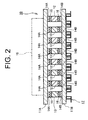
- the Peltier device 10 has a first board 11A and a second board 11B facing each other.
- the second board 11 B serves as the wiring board of the present invention.
- Ceramic material such as aluminum nitride (AIN) is preferably used for the material of the first and second boards 11A and 11B.
- the ceramic material has a lower coefficient of thermal expansion than metal, also has electrical insulation properties, and further has a higher coefficient of thermal conductivity than aluminum oxide.
- a plurality of P type semiconductor devices 12 and N type semiconductor devices 13 are disposed alternately between the first and second boards 11A and 11B. Referring to Figs.
- a plurality of electrodes 14A is formed on the inner surface of the first board 11A by etching of copper plating and a plurality of electrodes 14B is formed on the inner surface of the second board 11B by etching of copper plating.
- Each electrode 14B serves as the conductor layer of the present invention.
- Aluminum may be used instead of copper for the electrodes 14A and 14B, in which case the electrodes 14A and 14B are formed by brazing rather than by etching.
- the vertical direction and lateral direction as seen in the drawing correspond to the longitudinal direction and width direction of the second board 11 B, respectively.
- the electrodes 14B except the four electrodes 14B at the top in the drawing, has such a rectangular shape in plan view that the dimension along the longitudinal direction (or the direction of length) of the second board 11B is larger than the dimension along the width direction (or the direction of width).
- the electrodes 14B are arranged in a regular manner on the second board 11 B.
- the electrodes 14B are arranged on the inner surface of the second board 11B in such orientation that the longitudinal directions of the electrodes 14B coincide with the longitudinal direction of the second board 11 B.
- electrodes 14B at the rear end are arranged in such orientation that their longitudinal directions coincide with the width direction of the second board 11B.
- the intervals of the electrodes 14B in the respective longitudinal direction and width direction of the second board 11 B are set substantially the same.
- the electrodes 14A of the first board 11A are arranged in a regular manner on the first board 11A as in the case of the electrodes 14B of the second board 11B. It is noted that the electrodes 14A at the front end (or at the lower end of Fig. 3 ) on the first board 11 A are arranged in such orientation that their longitudinal directions coincide with the width direction of the first board 11A. The other electrodes 14A are arranged on the inner surface of the first board 11A in such orientation that the longitudinal directions of the electrode 14A coincide with the longitudinal direction of the first board 11A.
- the P type semiconductor devices 12 and the N type semiconductor devices 13 are electrically connected in series via the electrodes 14A and 148.
- Each P type semiconductor device 12 is joined at one surface thereof to the first board 11A via the corresponding electrode 14A and at the other surface thereof to the second board 11B via the corresponding electrode 14B.
- Each N type semiconductor device 13 is joined at one surface thereof to the first board 11A via the corresponding electrode 14A and at the other surface thereof to the second board 11B via the corresponding electrode 14B.
- a heat absorber 15 is joined to the outer surface (or the upper surface) of the first board 11A in Fig. 1 or 2
- radiator fins 17 are joined to the outer surface (or the lower surface) of the second board 11 B in Fig. 1 or 2 .
- the heat absorber 15 may be provided by absorber fins that have the same structure as the radiator fins 17.
- the heat absorber 15 and the radiator fins 17 may be replaced by the radiator and the absorber fins, respectively, by changing the direction of current flowing through both of the P type semiconductor devices 12 and the N type semiconductor devices 13.
- the radiator fins 17 serve as the fin of the present invention.
- the inner surface of the second board 11B facing the first board 11A serves as the first surface of the wiring board of the present invention and the outer surface of the second board 11B serves as the second surface of the wiring board of the present invention, respectively.
- each P type semiconductor device 12 are joined to the electrodes 14A and 14B via solder 16, respectively.
- the opposite surfaces of each N type semiconductor device 13 are joined to the electrodes 14A and 14B via solder 16, respectively.
- the Peltier device 10 heat is transferred between the P type semiconductor devices 12 and the N type semiconductor devices 13, so that a temperature difference occurs between the first board 11A and the second board 11 B and one of the first board 11A and the second board 11 B serves to absorb heat and the other serves to radiate heat.
- the heat absorber 15 is cooled and the radiator fins 17 are heated.
- the radiator fins 17 are an offset fin and made of copper that is the same as the material of the electrodes 14A and 14B.
- the radiator fins 17 are formed by bending a metal plate and have a base 18 and a plurality of projections 19 projecting from the base 18.
- the base 18 has a plurality of bottom walls 20 formed between the projections 19.
- Each projection 19 has a pair of vertical walls 21 that extends vertically from the bottom walls 20 and a top wall 22 that extends parallel to the bottom walls 20 to interconnect the distal ends of the paired vertical walls 21.
- the projections 19 are spaced in the width of the radiator fins 17 so as to form a plurality of longitudinal rows of projections extending in the longitudinal direction of the radiator fins 17 (or the direction along which the metal plate is bent).
- the rows of the projections 19 are spaced in the width direction of the radiator fins 17 so that the projections and recesses are formed alternately in the width direction of the radiator fins 17.
- radiator fins 17 are bent to have bent edges at the boundaries between each bottom wall 20 and the corresponding vertical walls 21 and also at the boundaries between each vertical wall 21 and the corresponding top wall 22.
- the vertical walls 21 and the bottom walls 20 of the radiator fins 17 serve to radiate heat.
- the vertical walls 21 and the bottom walls 20 of the radiator fins 17 serve as the heat transfer portion of the present invention.
- each longitudinal row of the projections 19 in each longitudinal row are formed continuously in an offset manner so that any two adjacent projections 19 are offset in the width direction of the radiator fins 17.
- Each top wall 22 of the radiator fins 17 serves as the joining portion of the present invention.
- the surface of each top wall 22 joined to the second board 11 B serves as the joining surface of the present invention.
- Each longitudinal row of the projections 19 has on the top walls 22 thereof a joining area T that extends in the longitudinal direction of the radiator fins 17 in a straight line with a constant width.
- the width of the joining area T is the same as that of each electrode 14B.
- there are overlap regions (indicated by shading in Fig.
- the radiator fins 17 and the electrodes 14B as viewed in thickness direction (or direction of thickness) of the second board 11B.
- Part of the top walls 22 of the radiator fins 17 is located in each overlap region as viewed in the thickness direction of the second board 11 B.
- the entire overlap regions are located in the top walls 22 as viewed in the thickness direction of the second board 11B.
- the ratio of the area of the joining surfaces of the top walls 22 that coincide with each overlap region to the area of the overlap region is set larger than that of the area of the joining surfaces of the top walls 22 that coincide with each separation region to the area of the separation region.
- the vertical walls 21 of the radiator fins 17 extend in the longitudinal direction of the radiator fins 17 have stiffness against bending across the longitudinal direction thereof to resist the deformation caused by the thermal stress.
- the radiator fins 17 having bent edges in the width direction thereof are elastically deformable in the width direction thereof. That is, the radiator fins 17 that are elastically deformable in the width direction thereof are hard to be elastically deformed across the longitudinal direction thereof by the stiffness.
- the top walls 22 are joined to the heat radiating surface of the second board 11B.
- a plurality of projections 19 of each row are formed continuously in the longitudinal direction of the electrode 14B.
- the longitudinal directions of the electrodes 14B coincide with the direction in which the bent edges of the radiator fins 17 extend.
- the direction in which any two adjacent projections 19 in each longitudinal row are offset coincides with the width direction of the electrodes 14A.
- the electrodes 14B and the top walls 22 are disposed in overlapping relation to each other across the second board 11B. That is, the top walls 22 are located so as to correspond to the electrodes 14B.
- the areas S of the electrodes 14B as projected in plan view are located within the joining area T in each row of projections 19, as shown in Figs. 3 and 4 .
- Each joining area T extends continuously in the longitudinal direction of the electrodes 14B.
- the following will describe in detail the heat radiation of the semiconductor unit according to the first embodiment.
- heat is transferred between the P type semiconductor devices 12 and the N type semiconductor devices 13 thereby to cause a temperature difference between the first board 11A and the second board 11B.
- the first board 11A serving to absorb heat is cooled while the second board 11 B serving to radiate heat is heated.
- the heat of the second board 11 B is transferred to the vertical walls 21 and the bottom walls 20 via the surfaces (or joining surfaces) of the top walls 22 joined to the second board 11B.
- the heat of the vertical walls 21 and the bottom walls 20 of the projections 19 of the radiator fins 17 is radiated to heat medium such as air or any other fluids flowing through the radiator fins 17.
- Heat generated by the electrodes 14B causes thermal stress to be developed in the second board 11B due to a relatively large difference in the coefficient of thermal expansion between the second board 11B and the electrodes 14B.
- the thermal stress causes deformation such as warp of the second board 11B.
- the electrodes 14B and the top walls 22 that are made of the same material develop thermal stresses of the same magnitude to the second board 11B thereby to cancel the deformation of the second board 11B caused by the thermal stresses, which prevents the deformation of the entire second board 11B.
- the heat of the electrodes 14B is transferred to the radiator fins 17.
- Thermal stress occurs in the outer surface of the second board 11B due to the difference in coefficient of thermal expansion between the second board 11B and the radiator fins 17.
- the thermal stress acting in the width direction of the second board 11 B and causing the deformation of the second board 11 B is absorbed by the elastic deformation of the radiator fins 17 in the width direction thereof.
- the thermal stress acting in the longitudinal direction of the electrodes 14B urges the second board 11 B to warp across the longitudinal direction of the second board 11 B, the stiffness of the radiator fins 17 in the longitudinal direction thereof resists the thermal stress causing the deformation of the second board 11B.
- thermal stress acting in the longitudinal direction of the electrodes 14B causes no deformation of the second board 11B.
- the areas S of the electrodes 14B as projected in plan view are located within the joining area T in each row of the projections 19.
- the heat of the electrodes 14B is rapidly transferred to the radiator fins 17 via the joining areas T corresponding to the respective electrodes 14B, which makes it easy to prevent the deformation of the second board 11 B caused by the thermal stress due to the difference in coefficient of thermal expansion between the second board 11 B and the electrodes 14B.
- the areas S of the electrodes 14B as projected in plan view are located within the joining area T extending in the longitudinal direction of the electrodes 14B in each row of the projections 19, and the electrodes 14B and the radiator fins 17 are both made of the same copper. If the joining areas T and the projected areas S of the electrodes 14B are the same in both area and shape, the top walls 22 and the electrodes 14B are the same in both thickness and material, and the joining areas T and the projected areas S of the electrodes 14B are disposed in overlapping relation to each other, the deformation of the second board 11 B caused by the thermal stress is canceled.
- the deformation of the second board 11B caused by the thermal stress generated by the respective electrodes 14B and the deformation of the second board 11 B caused by the thermal stress generated in the projected areas S of the electrodes 14B located in the joining areas T are approximate to each other. That is, the thermal stress generated by the electrodes 14B and causing the deformation of the second board 11 B is substantially canceled by the thermal stress generated by the electrodes 14B in the projected areas S and causing the deformation of the second board 11B. Consequently, the deformation of the second board 11B is prevented.
- the radiator fins 17 In fixing the radiator fins 17 to the second board 11B by soldering, the radiator fins 17 absorb by its elastic deformation the thermal stress in the width direction of the electrodes 14B caused by soldering and resists the thermal stress in the longitudinal direction of the electrodes 14B by its stiffness. Thus, the deformation of the second board 11B is prevented in the same manner as in the case when the Peltier device 10 is in operation.
- the radiator fins 17A of the semiconductor unit are a straight fin having a plurality of straight projections 19 extending in the longitudinal direction (or in the direction of the bent edge) of the radiator fins 17A.
- the projections 19 are juxtaposed in the width direction of the radiator fins 17A (or in the direction perpendicular to the direction of the bent edge).
- there are overlap regions (indicated by shading in Fig. 5A ) between the radiator fins 17A and the electrodes 14B as viewed in thickness direction of the second board 11B.
- Part of the top walls 22 of the radiator fins 17A is located in each overlap region as viewed in the thickness direction of the second board 11B.
- the entire overlap regions are located in the top walls 22 of the radiator fins 17A as viewed in the thickness direction of the second board 11 B.
- Each projection 19 of the radiator fins 17A has a pair of vertical walls 21 that extends vertically from the bottom walls 20 and a top wall 22 that extends parallel to the bottom walls 20 to interconnect the distal ends of the paired vertical walls 21.
- the entire joining surfaces of the top walls 22 joined to the electrodes 14B correspond to the joining areas T and the width of the top wall 22 is the same as that of the electrodes 14B.
- a plurality of areas S of the electrodes 14B as projected in plan view is located in each joining area T or on each top wall 22.
- the radiator fins 17A having in the width direction thereof a plurality of bent edges extending along the longitudinal direction of the radiator fins 17A are elastically deformable in the width direction thereof and has stiffness against bending across the longitudinal direction thereof.
- radiator fins 17B through 17D of the semiconductor units are a straight fin as in the case of the first modification of Figs. 5A and 5B .
- the radiator fins 17B of Fig. 6A are formed with the spaced distance between the opposed vertical walls 21 of any two adjacent projections 19 in the width direction of the radiator fins 17B set half the corresponding interval in the case of the first modification.
- the second modification there are overlap regions between the radiator fins 17B and the electrodes 14B as viewed in thickness direction of the second board 11B.
- the ratio of the area of the joining surface of the top wall 22 that coincides with each overlap region to the area of the overlap region is 1/2.
- the ratio of the area of the joining surface of the top wall 22 that coincides with each overlap region to the area of the overlap region is the same as that of the area of the joining surface of the top wall 22 that coincides with each separation region to the area of the separation region.
- the projections 19 of the radiator fins 17C are spaced at two different intervals. More specifically, when there are overlap regions between the radiator fins 17C and the electrodes 14B as viewed in thickness direction of the second board 11B, the radiator fins 17C are formed at the overlap regions with the spaced distance between the opposed vertical walls 21 of any two adjacent projections 19 in the width direction of the radiator fins 17C set one third the corresponding interval in the case of the first modification.
- the radiator fins 17C are formed at the separation regions with the spaced distance between the opposed vertical walls 21 in the width direction of the radiator fins 17C set the same as the corresponding interval in the case of the first modification.
- narrow bottom walls 20A and broad bottom walls 20B are formed in the radiator fins 17C as shown in Fig. 6B .
- the ratio of the area of the joining surface of the top wall 22 that coincides with each overlap region to the area of the overlap region is 2/3.
- the ratio of the area of the joining surface of the top wall 22 that coincides with each overlap region to the area of the overlap region is set larger than that of the area of the joining surface of the top wall 22 that coincides with each separation region to the area of the separation region.
- the projections 19 of the radiator fins 17D are spaced at an interval that is twice as large as that in the case of the first modification of Fig. 5B .
- the electrode 14B does not overlap with the entirety of its corresponding top wall 22 of the radiator fins 17D across the second board 118 as viewed in the thickness direction of the second board 11B.
- the radiator fins 17D are formed in such a way that the electrodes 14B overlapping with the top wall 22 of the radiator fins 17D across the second board 11 B alternate with the electrodes 14B overlapping with no top wall 22 of the radiator fins 17D.
- each of the radiator fins 17A-17D of the first through fourth modifications absorbs the deformation caused by the thermal stress in the width direction of the electrodes 14B by its elastic deformation and resists the deformation caused by the thermal stress in the longitudinal direction of the electrodes 14B by its stiffness. Thus, the deformation of the second board 11 B is prevented.
- the second embodiment differs from the first embodiment in that the radiator fins 27 corresponding to the radiator fins 17 of the first embodiment are elastically deformable not only in the width direction of the radiator fins 27 but also in the longitudinal direction of the radiator fins 27. Since the second embodiment is the same as the first embodiment in structure other than the radiator fins, the description about the common elements or parts of the second embodiment is omitted by incorporating the description of the first embodiment and the same reference numerals of the first embodiment are used for the common elements or parts of the first and second embodiments.
- the radiator fins 27 are made of copper that is used for the electrodes 14A and 14B.
- the radiator fins 17 are formed by bending a metal plate and have a base 28 and a plurality of projections 29 projecting from the base 28.
- each projection 29 has a pair of vertical walls 31 that vertically extends from the bottom walls 30 and a top wall 32 that extends parallel to the bottom walls 30 to interconnect the distal ends of the paired vertical walls 31.
- the projections 29 are formed at intervals in width direction of the radiator fins 27.
- the radiator fins 27 are formed with a series of alternate square projections and square recesses in the width direction of the radiator fins 27.
- the radiator fins 27 are bent to have bent edges at the boundaries between each bottom wall 30 and the corresponding vertical walls 31 and also at the boundaries between each vertical wall 31 and the corresponding top wall 32.
- the vertical walls 31 and the bottom walls 30 of the radiator fins 27 serve to radiate heat.
- the vertical walls 31 and the bottom walls 30 of the radiator fins 27 serve as the heat transfer portion of the present invention.
- the paired vertical walls 31 of the radiator fins 27 in the present embodiment are bent in a zigzag manner in the direction of the bent edge of the radiator fins 27.
- the paired vertical walls 31 are spaced so that the width of the bottom wall 30 is constant and that the width of the top wall 32 is also constant.
- the top wall 32 is formed in a zigzag manner in the longitudinal direction of the entire bent edges of the radiator fins 27 in a planar view of the radiator fins 27.
- the longitudinal direction of the entire bent edges of the radiator fins 27 serves as the direction in which the bent edge of the present invention extends.
- Each projection 29 of the radiator fins 27 has on the top wall 32 thereof a joining area T that extends in the longitudinal direction with a constant width.
- the width of the joining area T is the same as that of the electrode 14B.
- Part of the top walls 22 of the radiator fins 27 is located in each overlap region as viewed in the thickness direction of the second board 11 B.
- the entire overlap regions are located in the top walls 22 as viewed in the thickness direction of the second board 11B.
- the ratio of the area of the joining surface of the top wall 32 that coincides with each overlap region to the area of the overlap region is set larger than that of the area of the joining surface of the top wall 32 that coincides with each separation region to the area of the separation region.
- the vertical walls 31 which are bent in a zigzag manner in the longitudinal direction of the radiator fins 27 are elastically deformable in the longitudinal direction of the radiator fins 27.
- the radiator fins 27 are elastically deformable not only in the width direction of the radiator fins 27 but also in the longitudinal direction of the radiator fins 27. It is noted that the thickness of the radiator fins 27 is set larger than that of the radiator fins 17 of the first embodiment.
- radiator fins 27 With the radiator fins 27 fixed to the second board 11B by brazing as shown in Fig. 8 , the top walls 32 are joined to the heat radiating surface of the second board 11B.
- Each projection 29 of the radiator fins 27 is formed extending continuously in the longitudinal directions of the electrodes 14B.
- the longitudinal directions of the electrodes 14B and the longitudinal direction of the entire bent edges of the radiator fins 27 are the same.
- the electrodes 14B and the top walls 32 are disposed in overlapping relation to each other across the second board 11 B. That is, the top wall 32 that serves as the joining portion of the present invention is located so as to correspond to the electrodes 14B.
- the area S of the electrodes 14B on the second board 11B as projected in plan view is located in the corresponding joining area T as shown in Figs. 7 and 8 .
- the joining area T is formed continuously in the longitudinal direction of the electrode 14B.
- the second embodiment offers substantially the same effects as the effects (2) through (5) of the first embodiment.
- the radiator fins 27 joined to the second board 11 B are elastically deformable in the longitudinal direction of the entire bent edges and also in the direction perpendicular to the longitudinal direction of the entire bent edges. It is noted that the degree of the elastic deformation (or the deformation amount per stress for a given stress level) in the direction perpendicular to the longitudinal direction of the entire bent edges is much larger than that of the elastic deformation in the longitudinal direction of the entire bent edges. That is, the radiator fins 27 have a certain level of stiffness against bending across the longitudinal direction of the radiator fins 27.
- the heat of the electrodes 14B of the second board 11 B is absorbed by the radiator fins 27 and then radiated from the radiator fins 27.
- the thermal stress acting in the width direction of the electrodes 14B and causing the deformation of the second board 11B is absorbed by the elastic deformation of the radiator fins 27 and the thermal stress acting in the longitudinal direction of the electrodes 14B and causing the deformation of the second board 11 B is resisted by the stiffness of the radiator fins 27.
- the deformation of the second board 11B is prevented.
- the thermal stress occurring in the outer surface of the second board 11 B may become larger than the thermal stress occurring in the inner surface of the second board 11 B.
- the second board 11B may not resist the thermal stress acting in the longitudinal direction of the radiator fins 27 and causing the deformation.
- the radiator fins 27 of the present embodiment however, the radiator fins 27 are deformed in the longitudinal direction thereof so that the thermal stress occurring in the inner surface of the second board 11B becomes the same as the thermal stress occurring in the outer surface of the second board 11B. Thus, the deformation of the second board 11B is prevented.
- the radiator fins 17 may be formed in accordance with the relation between the thickness of the radiator fins and the thickness of the second board 11B having the electrodes 14B so as to have stiffness that resists the thermal stress acting in the longitudinal direction of the radiator fins 17 and causing the deformation of the second board 11 B as in the case of the first embodiment.
- the radiator fins 27 may be formed so as to be elastically deformable in the longitudinal direction of the radiator fins 27 as in the case of the second embodiment.
- the radiator fins 17 may be formed so as to be elastically deformable in the longitudinal direction of the radiator fins 17 as in the case of the second embodiment.
- the second board 11B is prevented from being warped.
- the electrodes 14B and the projections 29 may be arranged otherwise.
- the radiator fins may be formed so that each projection is bent with a large angle toward the width direction of the radiator fins and also that one projection corresponds to two rows of the electrodes 14B.
- the electrodes 14B and the projections 29 are of two-to-one correspondence.
- a plurality of grooves formed in the longitudinal direction of the second board 11B are formed in the surface of the second board 11B to which radiator fins 37 corresponding to the radiator fins 17 of the first embodiment are fixed.
- the grooves are formed in the width direction of the second board 11B.
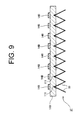
- the radiator fins 37 are of a triangular fin which is formed in a zigzag manner as viewed in longitudinal direction of the radiator fins 37.
- the radiator fins 37 do not have substantially the bottom walls and the top walls of the first embodiment, but have inclined walls.
- a plurality of electrodes 14B each serving as the conductor layer of the present invention are formed on one surface (or the first surface) of the second board 11B and the radiator fins 37 are joined to the other or outer surface (or the second surface) of the second board 11B.
- the surface of the second board 11B to which the radiator fins 37 are fixed has a plurality of grooves 111 disposed in the width direction of the second board 11B.
- Each groove 111 has a V shape as viewed in the longitudinal direction of the second board 11B.
- each groove 111 is formed across the length of the radiator fins 37 thereby to improve the bending strength against the thermal stress in the longitudinal direction of the radiator fins 37.
- the radiator fins 37 have a plurality of bent edges, the radiator fins 37 have substantially no bottom wall and no top wall unlike the first embodiment.
- the radiator fins 37 are formed by bending a metal plate and have walls 38 formed continuously and inclined in alternate directions.
- the bent edges of the radiator fins 37 form the top and bottom of the radiator fins 37.
- the distance between any two adjacent tops of the radiator fins 37 is the same as the distance between the any two adjacent grooves 111 of the second board 11B.
- the radiator fins 37 are fixed to the second board 11B with the radiator fins 37 inserted at the top thereof in the grooves 111 of the second board 11B. With the radiator fins 37 thus inserted in the grooves 111 of the second board 11B, the radiator fins 37 and the second board 11 B are in surface-to-surface contact with each other. The joint strength between the second board 11 B and the radiator fins 37 by surface-to-surface contact is greater than the strength by line contact.
- the radiator fins 37 having substantially no top wall may be fixed to the second board 11B.
- the bending strength against the thermal stress in the longitudinal direction of the radiator fins 37 is improved. Thus, the deformation caused by the thermal stress is prevented.
- Forming the grooves 111 in the second board 11B is not limited to the case of the radiator fins 37. In the fin having a small stiffness in the longitudinal direction of the second board 11 B, forming the grooves 111 in the second board 11 B is effective in reducing the deformation across the longitudinal direction of the second board 11B.
- the cross sectional shape of the groove is not limited and the shape of the joined radiator fins is freely determined.
- Radiator fins 17, 17A-17D and 27 having the top walls as in the cases of the first and second embodiments (including the modifications) may be used instead of the radiator fins 37 in the third embodiment.
- grooves are formed in the second board 11 B with a shape that conforms to the respective top walls of the radiator fins 17, 17A-17D and 27.
- the board (or the second board) of the Peltier device is used for the wiring board
- any wiring board having a radiator element other than Peltier device may be used.
- Any wiring board having a transformer or a power controlling electronic component may be used.
- any one of the offset fin, the straight fin and the triangular fin is used as the radiator fins, such fins as herringbone fin, perforated fin or serrated fin may be used.
- the shape of the conductor layer is not limited to a rectangle. According to the present invention, the conductor layer is required to have a dimension that extends in longitudinal direction.
- the shape of conductor layer excludes regular polygon such as square and circle having no longitudinal direction but includes a rectangle and an oval.
- the materials of the radiator fins and the conductor layer are the same, the materials of the radiator fins and the conductor layer may be different. Any material may be used for the radiator fins and the conductor layer as long as the thermal stress generated between the joining surface of the radiator fins and the wiring board and the thermal stress generated between the conductor layer and the wiring board are distributed so as to cancel each other.
- the width of the joining portion (joining area T) of the radiator fins is substantially the same as that of the conductor layer (the projected area S on the surface of electrode), the width of the joining portion of the radiator fins does not need to be the same as that of the conductor layer as long as the thermal stress generated between the joining surface of the radiator fins and the wiring board and the thermal stress generated between the conductor layer and the wiring board are distributed so as to cancel each other.
- the absorber fins that serve also as the fin of the present invention may be used by changing the direction of current flowing through the Peltier device. In the case of the absorber fins wherein the heat transfer occurs in opposite direction, the same effect as in the case of the radiator fins may be accomplished.
Landscapes
- Physics & Mathematics (AREA)
- Thermal Sciences (AREA)
- Engineering & Computer Science (AREA)
- Microelectronics & Electronic Packaging (AREA)
- Cooling Or The Like Of Semiconductors Or Solid State Devices (AREA)
- Cooling Or The Like Of Electrical Apparatus (AREA)
- Structure Of Printed Boards (AREA)
Applications Claiming Priority (1)
| Application Number | Priority Date | Filing Date | Title |
|---|---|---|---|
| JP2010200047A JP2012059831A (ja) | 2010-09-07 | 2010-09-07 | 配線基板の伝熱装置 |
Publications (1)
| Publication Number | Publication Date |
|---|---|
| EP2426748A1 true EP2426748A1 (fr) | 2012-03-07 |
Family
ID=44772745
Family Applications (1)
| Application Number | Title | Priority Date | Filing Date |
|---|---|---|---|
| EP11179813A Withdrawn EP2426748A1 (fr) | 2010-09-07 | 2011-09-02 | Unité de semi-conducteur |
Country Status (6)
| Country | Link |
|---|---|
| US (1) | US20120057305A1 (fr) |
| EP (1) | EP2426748A1 (fr) |
| JP (1) | JP2012059831A (fr) |
| KR (1) | KR20120025432A (fr) |
| CN (1) | CN102403285A (fr) |
| TW (1) | TW201214637A (fr) |
Cited By (1)
| Publication number | Priority date | Publication date | Assignee | Title |
|---|---|---|---|---|
| WO2021045516A1 (fr) | 2019-09-04 | 2021-03-11 | Lg Innotek Co., Ltd. | Module thermoélectrique |
Families Citing this family (10)
| Publication number | Priority date | Publication date | Assignee | Title |
|---|---|---|---|---|
| CN104205382A (zh) | 2012-01-25 | 2014-12-10 | 阿尔法贝特能源公司 | 用于热回收系统的模块化热电单元及其方法 |
| US9257627B2 (en) | 2012-07-23 | 2016-02-09 | Alphabet Energy, Inc. | Method and structure for thermoelectric unicouple assembly |
| US9065017B2 (en) | 2013-09-01 | 2015-06-23 | Alphabet Energy, Inc. | Thermoelectric devices having reduced thermal stress and contact resistance, and methods of forming and using the same |
| US20150287901A1 (en) * | 2013-10-14 | 2015-10-08 | Alphabet Energy, Inc. | Flexible lead frame for multi-leg package assembly |
| TWI563909B (en) * | 2016-01-29 | 2016-12-21 | Delta Electronics Inc | Thermo electric heat dissipation module |
| JP6909062B2 (ja) * | 2017-06-14 | 2021-07-28 | 株式会社Kelk | 熱電モジュール |
| KR102693401B1 (ko) * | 2019-09-04 | 2024-08-09 | 엘지이노텍 주식회사 | 열전모듈 |
| KR102690013B1 (ko) * | 2019-09-04 | 2024-08-01 | 엘지이노텍 주식회사 | 열전모듈 |
| WO2021194111A1 (fr) * | 2020-03-23 | 2021-09-30 | 엘지이노텍 주식회사 | Dispositif thermoélectrique |
| US12581855B2 (en) * | 2020-07-24 | 2026-03-17 | Lg Innotek Co., Ltd. | Thermoelectric module |
Citations (4)
| Publication number | Priority date | Publication date | Assignee | Title |
|---|---|---|---|---|
| JPS572664U (fr) | 1980-06-06 | 1982-01-08 | ||
| JPS6435788U (fr) | 1987-08-27 | 1989-03-03 | ||
| US20030102554A1 (en) * | 2001-10-11 | 2003-06-05 | Rencai Chu | Thermoelectric module |
| US20090014046A1 (en) * | 2007-07-12 | 2009-01-15 | Industrial Technology Research Institute | Flexible thermoelectric device and manufacturing method thereof |
Family Cites Families (10)
| Publication number | Priority date | Publication date | Assignee | Title |
|---|---|---|---|---|
| US5225964A (en) * | 1991-10-31 | 1993-07-06 | Rockwell International Corporation | Integrated lightweight card rack |
| JP3451107B2 (ja) * | 1992-10-05 | 2003-09-29 | 株式会社エコ・トゥエンティーワン | 電子冷却装置 |
| JP3158983B2 (ja) * | 1994-10-03 | 2001-04-23 | 住友精密工業株式会社 | Lsiパッケージ冷却用コルゲート型放熱フィン |
| JP3369349B2 (ja) * | 1995-03-02 | 2003-01-20 | 株式会社エコ・トゥエンティーワン | 熱電変換装置 |
| US5648892A (en) * | 1995-09-29 | 1997-07-15 | Allen-Bradley Company, Inc. | Wireless circuit board system for a motor controller |
| JP4231610B2 (ja) * | 2000-02-09 | 2009-03-04 | サンデン株式会社 | 熱交換器用フィンの製造方法 |
| JP2006156818A (ja) * | 2004-11-30 | 2006-06-15 | Denso Corp | 熱電変換装置およびその熱電変換装置の製造方法 |
| JP4756585B2 (ja) * | 2005-09-09 | 2011-08-24 | 臼井国際産業株式会社 | 熱交換器用伝熱管 |
| US7436059B1 (en) * | 2006-11-17 | 2008-10-14 | Sun Microsystems, Inc. | Thermoelectric cooling device arrays |
| CN201199528Y (zh) * | 2008-04-03 | 2009-02-25 | 无锡职业技术学院 | 一种新型半导体制冷制热装置 |
-
2010
- 2010-09-07 JP JP2010200047A patent/JP2012059831A/ja not_active Withdrawn
-
2011
- 2011-08-24 US US13/216,689 patent/US20120057305A1/en not_active Abandoned
- 2011-09-02 EP EP11179813A patent/EP2426748A1/fr not_active Withdrawn
- 2011-09-05 CN CN2011102643172A patent/CN102403285A/zh active Pending
- 2011-09-05 TW TW100131846A patent/TW201214637A/zh unknown
- 2011-09-06 KR KR1020110089980A patent/KR20120025432A/ko not_active Ceased
Patent Citations (4)
| Publication number | Priority date | Publication date | Assignee | Title |
|---|---|---|---|---|
| JPS572664U (fr) | 1980-06-06 | 1982-01-08 | ||
| JPS6435788U (fr) | 1987-08-27 | 1989-03-03 | ||
| US20030102554A1 (en) * | 2001-10-11 | 2003-06-05 | Rencai Chu | Thermoelectric module |
| US20090014046A1 (en) * | 2007-07-12 | 2009-01-15 | Industrial Technology Research Institute | Flexible thermoelectric device and manufacturing method thereof |
Cited By (3)
| Publication number | Priority date | Publication date | Assignee | Title |
|---|---|---|---|---|
| WO2021045516A1 (fr) | 2019-09-04 | 2021-03-11 | Lg Innotek Co., Ltd. | Module thermoélectrique |
| EP4026176A4 (fr) * | 2019-09-04 | 2023-09-13 | LG Innotek Co., Ltd. | Module thermoélectrique |
| US11974503B2 (en) | 2019-09-04 | 2024-04-30 | Lg Innotek Co., Ltd. | Thermoelectric module |
Also Published As
| Publication number | Publication date |
|---|---|
| JP2012059831A (ja) | 2012-03-22 |
| KR20120025432A (ko) | 2012-03-15 |
| US20120057305A1 (en) | 2012-03-08 |
| TW201214637A (en) | 2012-04-01 |
| CN102403285A (zh) | 2012-04-04 |
Similar Documents
| Publication | Publication Date | Title |
|---|---|---|
| EP2426748A1 (fr) | Unité de semi-conducteur | |
| CN204375726U (zh) | 液冷式冷却装置及液冷式冷却装置用散热器 | |
| CN101312168B (zh) | 半导体器件 | |
| JP6738226B2 (ja) | 冷却装置 | |
| JP7111010B2 (ja) | インバータ | |
| JPH0563244A (ja) | 熱電変換装置 | |
| JP5228115B2 (ja) | ヒートシンク | |
| US11881444B2 (en) | Semiconductor device | |
| EP3454367B1 (fr) | Module semi-conducteur | |
| JP6595531B2 (ja) | ヒートシンクアッセンブリ | |
| JP2012227472A (ja) | 電子部品の実装構造体 | |
| KR20150038121A (ko) | 방열판 | |
| CN101320715A (zh) | 半导体器件 | |
| JP6102676B2 (ja) | 半導体装置 | |
| JP6003109B2 (ja) | パワーモジュール | |
| JP6872976B2 (ja) | 電力半導体装置、及び電力変換装置 | |
| CN100452393C (zh) | 存储器模块 | |
| JP2010021410A (ja) | サーモモジュール | |
| TWI566670B (zh) | 散熱裝置 | |
| WO2013002423A1 (fr) | Modules de conversion thermoélectrique | |
| JP5793295B2 (ja) | 半導体装置 | |
| JP3449285B2 (ja) | 熱歪吸収体およびそれを用いたパワー半導体装置 | |
| JP2012079912A (ja) | 基材の放熱フィン | |
| CN101499467A (zh) | 热电模块 | |
| JP4151265B2 (ja) | 放熱器 |
Legal Events
| Date | Code | Title | Description |
|---|---|---|---|
| 17P | Request for examination filed |
Effective date: 20110902 |
|
| AK | Designated contracting states |
Kind code of ref document: A1 Designated state(s): AL AT BE BG CH CY CZ DE DK EE ES FI FR GB GR HR HU IE IS IT LI LT LU LV MC MK MT NL NO PL PT RO RS SE SI SK SM TR |
|
| AX | Request for extension of the european patent |
Extension state: BA ME |
|
| PUAI | Public reference made under article 153(3) epc to a published international application that has entered the european phase |
Free format text: ORIGINAL CODE: 0009012 |
|
| GRAP | Despatch of communication of intention to grant a patent |
Free format text: ORIGINAL CODE: EPIDOSNIGR1 |
|
| STAA | Information on the status of an ep patent application or granted ep patent |
Free format text: STATUS: THE APPLICATION IS DEEMED TO BE WITHDRAWN |
|
| 18D | Application deemed to be withdrawn |
Effective date: 20130416 |