EP2428986B1 - Réduction de la capacité de jonction des transistors par encastrement des régions de drain et de source - Google Patents
Réduction de la capacité de jonction des transistors par encastrement des régions de drain et de source Download PDFInfo
- Publication number
- EP2428986B1 EP2428986B1 EP11192120.1A EP11192120A EP2428986B1 EP 2428986 B1 EP2428986 B1 EP 2428986B1 EP 11192120 A EP11192120 A EP 11192120A EP 2428986 B1 EP2428986 B1 EP 2428986B1
- Authority
- EP
- European Patent Office
- Prior art keywords
- transistor
- drain
- source regions
- semiconductor
- semiconductor alloy
- Prior art date
- Legal status (The legal status is an assumption and is not a legal conclusion. Google has not performed a legal analysis and makes no representation as to the accuracy of the status listed.)
- Active
Links
Images



Classifications
-
- H—ELECTRICITY
- H10—SEMICONDUCTOR DEVICES; ELECTRIC SOLID-STATE DEVICES NOT OTHERWISE PROVIDED FOR
- H10P—GENERIC PROCESSES OR APPARATUS FOR THE MANUFACTURE OR TREATMENT OF DEVICES COVERED BY CLASS H10
- H10P95/00—Generic processes or apparatus for manufacture or treatments not covered by the other groups of this subclass
- H10P95/90—Thermal treatments, e.g. annealing or sintering
-
- H—ELECTRICITY
- H10—SEMICONDUCTOR DEVICES; ELECTRIC SOLID-STATE DEVICES NOT OTHERWISE PROVIDED FOR
- H10D—INORGANIC ELECTRIC SEMICONDUCTOR DEVICES
- H10D30/00—Field-effect transistors [FET]
- H10D30/01—Manufacture or treatment
- H10D30/021—Manufacture or treatment of FETs having insulated gates [IGFET]
- H10D30/0223—Manufacture or treatment of FETs having insulated gates [IGFET] having source and drain regions or source and drain extensions self-aligned to sides of the gate
- H10D30/0227—Manufacture or treatment of FETs having insulated gates [IGFET] having source and drain regions or source and drain extensions self-aligned to sides of the gate having both lightly-doped source and drain extensions and source and drain regions self-aligned to the sides of the gate, e.g. lightly-doped drain [LDD] MOSFET or double-diffused drain [DDD] MOSFET
-
- H—ELECTRICITY
- H10—SEMICONDUCTOR DEVICES; ELECTRIC SOLID-STATE DEVICES NOT OTHERWISE PROVIDED FOR
- H10D—INORGANIC ELECTRIC SEMICONDUCTOR DEVICES
- H10D30/00—Field-effect transistors [FET]
- H10D30/01—Manufacture or treatment
- H10D30/021—Manufacture or treatment of FETs having insulated gates [IGFET]
- H10D30/027—Manufacture or treatment of FETs having insulated gates [IGFET] of lateral single-gate IGFETs
- H10D30/0275—Manufacture or treatment of FETs having insulated gates [IGFET] of lateral single-gate IGFETs forming single crystalline semiconductor source or drain regions resulting in recessed gates, e.g. forming raised source or drain regions
-
- H—ELECTRICITY
- H10—SEMICONDUCTOR DEVICES; ELECTRIC SOLID-STATE DEVICES NOT OTHERWISE PROVIDED FOR
- H10D—INORGANIC ELECTRIC SEMICONDUCTOR DEVICES
- H10D30/00—Field-effect transistors [FET]
- H10D30/01—Manufacture or treatment
- H10D30/021—Manufacture or treatment of FETs having insulated gates [IGFET]
- H10D30/031—Manufacture or treatment of FETs having insulated gates [IGFET] of thin-film transistors [TFT]
- H10D30/0321—Manufacture or treatment of FETs having insulated gates [IGFET] of thin-film transistors [TFT] comprising silicon, e.g. amorphous silicon or polysilicon
- H10D30/0323—Manufacture or treatment of FETs having insulated gates [IGFET] of thin-film transistors [TFT] comprising silicon, e.g. amorphous silicon or polysilicon comprising monocrystalline silicon
-
- H—ELECTRICITY
- H10—SEMICONDUCTOR DEVICES; ELECTRIC SOLID-STATE DEVICES NOT OTHERWISE PROVIDED FOR
- H10D—INORGANIC ELECTRIC SEMICONDUCTOR DEVICES
- H10D30/00—Field-effect transistors [FET]
- H10D30/60—Insulated-gate field-effect transistors [IGFET]
- H10D30/67—Thin-film transistors [TFT]
- H10D30/6704—Thin-film transistors [TFT] having supplementary regions or layers in the thin films or in the insulated bulk substrates for controlling properties of the device
- H10D30/6713—Thin-film transistors [TFT] having supplementary regions or layers in the thin films or in the insulated bulk substrates for controlling properties of the device characterised by the properties of the source or drain regions, e.g. compositions or sectional shapes
- H10D30/6715—Thin-film transistors [TFT] having supplementary regions or layers in the thin films or in the insulated bulk substrates for controlling properties of the device characterised by the properties of the source or drain regions, e.g. compositions or sectional shapes characterised by the doping profiles, e.g. having lightly-doped source or drain extensions
-
- H—ELECTRICITY
- H10—SEMICONDUCTOR DEVICES; ELECTRIC SOLID-STATE DEVICES NOT OTHERWISE PROVIDED FOR
- H10D—INORGANIC ELECTRIC SEMICONDUCTOR DEVICES
- H10D30/00—Field-effect transistors [FET]
- H10D30/60—Insulated-gate field-effect transistors [IGFET]
- H10D30/67—Thin-film transistors [TFT]
- H10D30/6729—Thin-film transistors [TFT] characterised by the electrodes
-
- H—ELECTRICITY
- H10—SEMICONDUCTOR DEVICES; ELECTRIC SOLID-STATE DEVICES NOT OTHERWISE PROVIDED FOR
- H10D—INORGANIC ELECTRIC SEMICONDUCTOR DEVICES
- H10D30/00—Field-effect transistors [FET]
- H10D30/60—Insulated-gate field-effect transistors [IGFET]
- H10D30/791—Arrangements for exerting mechanical stress on the crystal lattice of the channel regions
- H10D30/797—Arrangements for exerting mechanical stress on the crystal lattice of the channel regions being in source or drain regions, e.g. SiGe source or drain
-
- H—ELECTRICITY
- H10—SEMICONDUCTOR DEVICES; ELECTRIC SOLID-STATE DEVICES NOT OTHERWISE PROVIDED FOR
- H10D—INORGANIC ELECTRIC SEMICONDUCTOR DEVICES
- H10D62/00—Semiconductor bodies, or regions thereof, of devices having potential barriers
- H10D62/01—Manufacture or treatment
- H10D62/021—Forming source or drain recesses by etching e.g. recessing by etching and then refilling
-
- H—ELECTRICITY
- H10—SEMICONDUCTOR DEVICES; ELECTRIC SOLID-STATE DEVICES NOT OTHERWISE PROVIDED FOR
- H10D—INORGANIC ELECTRIC SEMICONDUCTOR DEVICES
- H10D86/00—Integrated devices formed in or on insulating or conducting substrates, e.g. formed in silicon-on-insulator [SOI] substrates or on stainless steel or glass substrates
- H10D86/01—Manufacture or treatment
-
- H—ELECTRICITY
- H10—SEMICONDUCTOR DEVICES; ELECTRIC SOLID-STATE DEVICES NOT OTHERWISE PROVIDED FOR
- H10D—INORGANIC ELECTRIC SEMICONDUCTOR DEVICES
- H10D86/00—Integrated devices formed in or on insulating or conducting substrates, e.g. formed in silicon-on-insulator [SOI] substrates or on stainless steel or glass substrates
- H10D86/201—Integrated devices formed in or on insulating or conducting substrates, e.g. formed in silicon-on-insulator [SOI] substrates or on stainless steel or glass substrates the substrates comprising an insulating layer on a semiconductor body, e.g. SOI
-
- H—ELECTRICITY
- H10—SEMICONDUCTOR DEVICES; ELECTRIC SOLID-STATE DEVICES NOT OTHERWISE PROVIDED FOR
- H10D—INORGANIC ELECTRIC SEMICONDUCTOR DEVICES
- H10D30/00—Field-effect transistors [FET]
- H10D30/01—Manufacture or treatment
- H10D30/021—Manufacture or treatment of FETs having insulated gates [IGFET]
- H10D30/0212—Manufacture or treatment of FETs having insulated gates [IGFET] using self-aligned silicidation
-
- H—ELECTRICITY
- H10—SEMICONDUCTOR DEVICES; ELECTRIC SOLID-STATE DEVICES NOT OTHERWISE PROVIDED FOR
- H10D—INORGANIC ELECTRIC SEMICONDUCTOR DEVICES
- H10D84/00—Integrated devices formed in or on semiconductor substrates that comprise only semiconducting layers, e.g. on Si wafers or on GaAs-on-Si wafers
- H10D84/01—Manufacture or treatment
- H10D84/0123—Integrating together multiple components covered by H10D12/00 or H10D30/00, e.g. integrating multiple IGBTs
- H10D84/0126—Integrating together multiple components covered by H10D12/00 or H10D30/00, e.g. integrating multiple IGBTs the components including insulated gates, e.g. IGFETs
- H10D84/0165—Integrating together multiple components covered by H10D12/00 or H10D30/00, e.g. integrating multiple IGBTs the components including insulated gates, e.g. IGFETs the components including complementary IGFETs, e.g. CMOS devices
- H10D84/0167—Manufacturing their channels
-
- H—ELECTRICITY
- H10—SEMICONDUCTOR DEVICES; ELECTRIC SOLID-STATE DEVICES NOT OTHERWISE PROVIDED FOR
- H10D—INORGANIC ELECTRIC SEMICONDUCTOR DEVICES
- H10D84/00—Integrated devices formed in or on semiconductor substrates that comprise only semiconducting layers, e.g. on Si wafers or on GaAs-on-Si wafers
- H10D84/01—Manufacture or treatment
- H10D84/0123—Integrating together multiple components covered by H10D12/00 or H10D30/00, e.g. integrating multiple IGBTs
- H10D84/0126—Integrating together multiple components covered by H10D12/00 or H10D30/00, e.g. integrating multiple IGBTs the components including insulated gates, e.g. IGFETs
- H10D84/0165—Integrating together multiple components covered by H10D12/00 or H10D30/00, e.g. integrating multiple IGBTs the components including insulated gates, e.g. IGFETs the components including complementary IGFETs, e.g. CMOS devices
- H10D84/017—Manufacturing their source or drain regions, e.g. silicided source or drain regions
-
- H—ELECTRICITY
- H10—SEMICONDUCTOR DEVICES; ELECTRIC SOLID-STATE DEVICES NOT OTHERWISE PROVIDED FOR
- H10D—INORGANIC ELECTRIC SEMICONDUCTOR DEVICES
- H10D84/00—Integrated devices formed in or on semiconductor substrates that comprise only semiconducting layers, e.g. on Si wafers or on GaAs-on-Si wafers
- H10D84/01—Manufacture or treatment
- H10D84/0123—Integrating together multiple components covered by H10D12/00 or H10D30/00, e.g. integrating multiple IGBTs
- H10D84/0126—Integrating together multiple components covered by H10D12/00 or H10D30/00, e.g. integrating multiple IGBTs the components including insulated gates, e.g. IGFETs
- H10D84/0165—Integrating together multiple components covered by H10D12/00 or H10D30/00, e.g. integrating multiple IGBTs the components including insulated gates, e.g. IGFETs the components including complementary IGFETs, e.g. CMOS devices
- H10D84/0188—Manufacturing their isolation regions
-
- H—ELECTRICITY
- H10—SEMICONDUCTOR DEVICES; ELECTRIC SOLID-STATE DEVICES NOT OTHERWISE PROVIDED FOR
- H10D—INORGANIC ELECTRIC SEMICONDUCTOR DEVICES
- H10D84/00—Integrated devices formed in or on semiconductor substrates that comprise only semiconducting layers, e.g. on Si wafers or on GaAs-on-Si wafers
- H10D84/01—Manufacture or treatment
- H10D84/02—Manufacture or treatment characterised by using material-based technologies
- H10D84/03—Manufacture or treatment characterised by using material-based technologies using Group IV technology, e.g. silicon technology or silicon-carbide [SiC] technology
- H10D84/038—Manufacture or treatment characterised by using material-based technologies using Group IV technology, e.g. silicon technology or silicon-carbide [SiC] technology using silicon technology, e.g. SiGe
-
- H—ELECTRICITY
- H10—SEMICONDUCTOR DEVICES; ELECTRIC SOLID-STATE DEVICES NOT OTHERWISE PROVIDED FOR
- H10P—GENERIC PROCESSES OR APPARATUS FOR THE MANUFACTURE OR TREATMENT OF DEVICES COVERED BY CLASS H10
- H10P30/00—Ion implantation into wafers, substrates or parts of devices
- H10P30/20—Ion implantation into wafers, substrates or parts of devices into semiconductor materials, e.g. for doping
- H10P30/202—Ion implantation into wafers, substrates or parts of devices into semiconductor materials, e.g. for doping characterised by the semiconductor materials
- H10P30/204—Ion implantation into wafers, substrates or parts of devices into semiconductor materials, e.g. for doping characterised by the semiconductor materials into Group IV semiconductors
-
- H—ELECTRICITY
- H10—SEMICONDUCTOR DEVICES; ELECTRIC SOLID-STATE DEVICES NOT OTHERWISE PROVIDED FOR
- H10P—GENERIC PROCESSES OR APPARATUS FOR THE MANUFACTURE OR TREATMENT OF DEVICES COVERED BY CLASS H10
- H10P30/00—Ion implantation into wafers, substrates or parts of devices
- H10P30/20—Ion implantation into wafers, substrates or parts of devices into semiconductor materials, e.g. for doping
- H10P30/208—Ion implantation into wafers, substrates or parts of devices into semiconductor materials, e.g. for doping of electrically inactive species
-
- H—ELECTRICITY
- H10—SEMICONDUCTOR DEVICES; ELECTRIC SOLID-STATE DEVICES NOT OTHERWISE PROVIDED FOR
- H10P—GENERIC PROCESSES OR APPARATUS FOR THE MANUFACTURE OR TREATMENT OF DEVICES COVERED BY CLASS H10
- H10P30/00—Ion implantation into wafers, substrates or parts of devices
- H10P30/20—Ion implantation into wafers, substrates or parts of devices into semiconductor materials, e.g. for doping
- H10P30/21—Ion implantation into wafers, substrates or parts of devices into semiconductor materials, e.g. for doping of electrically active species
-
- H—ELECTRICITY
- H10—SEMICONDUCTOR DEVICES; ELECTRIC SOLID-STATE DEVICES NOT OTHERWISE PROVIDED FOR
- H10P—GENERIC PROCESSES OR APPARATUS FOR THE MANUFACTURE OR TREATMENT OF DEVICES COVERED BY CLASS H10
- H10P30/00—Ion implantation into wafers, substrates or parts of devices
- H10P30/20—Ion implantation into wafers, substrates or parts of devices into semiconductor materials, e.g. for doping
- H10P30/222—Ion implantation into wafers, substrates or parts of devices into semiconductor materials, e.g. for doping characterised by the angle between the ion beam and the crystal planes or the main crystal surface
-
- H—ELECTRICITY
- H10—SEMICONDUCTOR DEVICES; ELECTRIC SOLID-STATE DEVICES NOT OTHERWISE PROVIDED FOR
- H10P—GENERIC PROCESSES OR APPARATUS FOR THE MANUFACTURE OR TREATMENT OF DEVICES COVERED BY CLASS H10
- H10P30/00—Ion implantation into wafers, substrates or parts of devices
- H10P30/20—Ion implantation into wafers, substrates or parts of devices into semiconductor materials, e.g. for doping
- H10P30/28—Ion implantation into wafers, substrates or parts of devices into semiconductor materials, e.g. for doping characterised by an annealing step, e.g. for activation of dopants
Definitions
- the depth of the recess 112A may be selected such that a certain amount of material of the layer 102 may be maintained above the buried insulating layer 103, while nevertheless a significant portion along the depth direction of the layer 102 may be refilled with a strained semiconductor alloy so as to exert a specific stress on the channel region 109 along a significant depth of the layer 102.
- a respective etch indicator species may be incorporated during the process for forming the strained semiconductor alloy 113.
- a respective indicator species may be added to the deposition ambient, thereby defining a moderately sharp boundary between portions having the indicator material and portions lacking the indicator material. Since, typically, deposition processes may be controlled with increased accuracy and may suffer from minor process fluctuations compared to respective etch processes, in this case, generally a reduced substrate-to-substrate variation of the recesses 117A may be achieved.
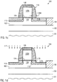
- Figure 1e schematically illustrates the semiconductor device 100 in a further advanced manufacturing stage, in which a further implantation process 118 is performed to define deep drain and source regions 115D that extend at least down to the buried insulating layer 103 with a moderately high dopant concentration, which may be accomplished due to the fact that a significant portion of the semiconductor material of the alloy 113 is missing.
- the implantation process 118 may result in a moderately high concentration across the entire depth of the deep drain and source regions 115D, providing the potential for avoiding complex implantation sequences with different implantation energies that may otherwise be necessary for providing the various concentration maxima at different depths of the corresponding semiconductor material.
Landscapes
- Thin Film Transistor (AREA)
- Insulated Gate Type Field-Effect Transistor (AREA)
- Metal-Oxide And Bipolar Metal-Oxide Semiconductor Integrated Circuits (AREA)
Claims (10)
- Dispositif semi-conducteur (200), comprenant :un premier transistor (200A) présentant une structure d'électrode de grille et des régions de drain et de source en renfoncement, lesdites régions de drain et de source étant disposées dans les parties en renfoncement d'une couche semi-conductrice (102) et s'étendant jusqu'à une couche isolante enterrée (103) ;un alliage semi-conducteur contraint (213A) disposé partiellement dans lesdites régions de drain et de source, ledit alliage semi-conducteur contraint (213A) induisant une contrainte dans une région canal (209) dudit premier transistor, une surface supérieure dudit alliage semi-conducteur contraint (213A) opposée à la couche isolante enterrée (103) étant en renfoncement en dessous d'une interface entre une couche d'isolation de grille (204) et la région canal (209) du premier transistor ;une structure espaceur (216) présentant une largeur ;un renfoncement dans l'une des régions de drain et de source en renfoncement ; etun matériau diélectrique d'intercouche formé au-dessus de la surface supérieure et dans une partie en renfoncement dudit alliage semi-conducteur contraint (213A),un bord du renfoncement étant décalé d'une paroi latérale de la structure d'électrode de grille d'une distance correspondant à la largeur de la structure espaceur (216).
- Dispositif semi-conducteur (200) selon la revendication 1, ledit alliage semi-conducteur contraint (213A) présentant une contrainte de compression ou une contrainte de traction.
- Dispositif semi-conducteur (200) selon la revendication 1, comprenant en outre un second transistor d'un type de conductivité différent par rapport audit premier transistor (200A), ledit second transistor présentant des régions de drain et de source sensiblement non en renfoncement.
- Dispositif semi-conducteur (200) selon la revendication 1, comprenant en outre un second transistor (200B) d'un type de conductivité différent par rapport audit premier transistor (200A), ledit second transistor (200B) présentant des régions de drain et de source en renfoncement s'étendant vers ladite couche isolante enterrée (103), ledit second transistor (200B) comprenant un alliage semi-conducteur contraint supplémentaire (213B) différant dudit alliage semi-conducteur (213A) dudit premier transistor (200A).
- Dispositif semi-conducteur (200) selon la revendication 1, ladite structure d'électrode de grille comprenant une partie électrode (205A), ladite partie électrode (205A) représentant une partie conductrice de la structure de l'électrode et présentant une longueur d'approximativement 50 nm et moins.
- Dispositif semi-conducteur (200) selon la revendication 1, présentant incorporée une espèce supplémentaire dans la couche semi-conductrice, l'espèce supplémentaire étant positionnée de sorte qu'elle ne s'étend pas vers la couche isolante enterrée (103).
- Dispositif semi-conducteur (200) selon la revendication 1, un profil latéral de dopant de régions profondes de drain et de source étant défini par ladite largeur de ladite structure espaceur (216).
- Dispositif semi-conducteur (200) selon la revendication 7, à l'intérieur des régions de drain et de source en dessous de la structure espaceur (216), l'alliage semi-conducteur contraint (213A) étant maintenu avec son épaisseur d'origine, fournissant ainsi un mécanisme efficace d'induction de contrainte dans la région canal (209).
- Dispositif semi-conducteur (200) selon la revendication 1, le matériau diélectrique d'intercouche étant disposé avec une contrainte intrinsèque pour augmenter la contrainte dans la région canal (209) sur la contrainte fournie dans la région canal (209) par ledit alliage semi-conducteur contraint (213A).
- Dispositif semi-conducteur (200) selon la revendication 1, une couche de siliciure métallique étant formée au niveau de la surface supérieure dudit alliage semi-conducteur contraint (213A), et le matériau diélectrique d'intercouche étant formé sur la couche de siliciure métallique dans la partie en renfoncement dudit alliage semi-conducteur contraint (213A).
Applications Claiming Priority (4)
| Application Number | Priority Date | Filing Date | Title |
|---|---|---|---|
| DE102007030053A DE102007030053B4 (de) | 2007-06-29 | 2007-06-29 | Reduzieren der pn-Übergangskapazität in einem Transistor durch Absenken von Drain- und Source-Gebieten |
| US12/027,583 US7754556B2 (en) | 2007-06-29 | 2008-02-07 | Reducing transistor junction capacitance by recessing drain and source regions |
| PCT/US2008/008150 WO2009005785A1 (fr) | 2007-06-29 | 2008-06-30 | Réduction d'une capacité de jonction de transistor par encastrement des régions de drain et de source |
| EP08794399A EP2168152B1 (fr) | 2007-06-29 | 2008-06-30 | Réduction d'une capacité de jonction de transistor par encastrement des régions de drain et de source |
Related Parent Applications (2)
| Application Number | Title | Priority Date | Filing Date |
|---|---|---|---|
| EP08794399.9 Division | 2008-06-30 | ||
| EP08794399A Division EP2168152B1 (fr) | 2007-06-29 | 2008-06-30 | Réduction d'une capacité de jonction de transistor par encastrement des régions de drain et de source |
Publications (3)
| Publication Number | Publication Date |
|---|---|
| EP2428986A2 EP2428986A2 (fr) | 2012-03-14 |
| EP2428986A3 EP2428986A3 (fr) | 2012-09-12 |
| EP2428986B1 true EP2428986B1 (fr) | 2018-08-22 |
Family
ID=40075974
Family Applications (2)
| Application Number | Title | Priority Date | Filing Date |
|---|---|---|---|
| EP08794399A Active EP2168152B1 (fr) | 2007-06-29 | 2008-06-30 | Réduction d'une capacité de jonction de transistor par encastrement des régions de drain et de source |
| EP11192120.1A Active EP2428986B1 (fr) | 2007-06-29 | 2008-06-30 | Réduction de la capacité de jonction des transistors par encastrement des régions de drain et de source |
Family Applications Before (1)
| Application Number | Title | Priority Date | Filing Date |
|---|---|---|---|
| EP08794399A Active EP2168152B1 (fr) | 2007-06-29 | 2008-06-30 | Réduction d'une capacité de jonction de transistor par encastrement des régions de drain et de source |
Country Status (8)
| Country | Link |
|---|---|
| US (2) | US7754556B2 (fr) |
| EP (2) | EP2168152B1 (fr) |
| JP (1) | JP5244908B2 (fr) |
| CN (1) | CN101755326B (fr) |
| AT (1) | ATE542238T1 (fr) |
| DE (1) | DE102007030053B4 (fr) |
| TW (1) | TWI471944B (fr) |
| WO (1) | WO2009005785A1 (fr) |
Families Citing this family (28)
| Publication number | Priority date | Publication date | Assignee | Title |
|---|---|---|---|---|
| DE102008011932B4 (de) * | 2008-02-29 | 2010-05-12 | Advanced Micro Devices, Inc., Sunnyvale | Verfahren zur Erhöhung der Eindringtiefe von Drain- und Sourceimplantationssorten für eine gegebene Gatehöhe |
| US7838308B2 (en) * | 2008-05-12 | 2010-11-23 | Advanced Micro Devices, Inc. | Method of controlling embedded material/gate proximity |
| DE102008035806B4 (de) * | 2008-07-31 | 2010-06-10 | Advanced Micro Devices, Inc., Sunnyvale | Herstellungsverfahren für ein Halbleiterbauelement bzw. einen Transistor mit eingebettetem Si/GE-Material mit einem verbesserten Boreinschluss sowie Transistor |
| DE102008054075B4 (de) * | 2008-10-31 | 2010-09-23 | Advanced Micro Devices, Inc., Sunnyvale | Halbleiterbauelement mit Abgesenktem Drain- und Sourcebereich in Verbindung mit einem Verfahren zur komplexen Silizidherstellung in Transistoren |
| US8216893B2 (en) | 2009-01-26 | 2012-07-10 | International Business Machines Corporation | Stress enhanced transistor devices and methods of making |
| KR20100087256A (ko) | 2009-01-26 | 2010-08-04 | 인터내셔널 비지네스 머신즈 코포레이션 | 개선된 트랜지스터 소자 및 제조 방법 |
| DE102009006884B4 (de) * | 2009-01-30 | 2011-06-30 | Advanced Micro Devices, Inc., Calif. | Verfahren zur Herstellung eines Transistorbauelementes mit In-Situ erzeugten Drain- und Source-Gebieten mit einer verformungsinduzierenden Legierung und einem graduell variierenden Dotierstoffprofil und entsprechendes Transistorbauelement |
| DE102009023298B4 (de) * | 2009-05-29 | 2012-03-29 | Globalfoundries Dresden Module One Limited Liability Company & Co. Kg | Verformungserhöhung in Transistoren mit einer eingebetteten verformungsinduzierenden Halbleiterlegierung durch Erzeugen von Strukturierungsungleichmäßigkeiten an der Unterseite der Gateelektrode |
| US9245805B2 (en) | 2009-09-24 | 2016-01-26 | Taiwan Semiconductor Manufacturing Company, Ltd. | Germanium FinFETs with metal gates and stressors |
| US8368127B2 (en) * | 2009-10-08 | 2013-02-05 | Globalfoundries Singapore Pte., Ltd. | Method of fabricating a silicon tunneling field effect transistor (TFET) with high drive current |
| US8368147B2 (en) | 2010-04-16 | 2013-02-05 | Taiwan Semiconductor Manufacturing Company, Ltd. | Strained semiconductor device with recessed channel |
| US8633096B2 (en) | 2010-11-11 | 2014-01-21 | International Business Machines Corporation | Creating anisotropically diffused junctions in field effect transistor devices |
| US8357579B2 (en) | 2010-11-30 | 2013-01-22 | Taiwan Semiconductor Manufacturing Company, Ltd. | Methods of forming integrated circuits |
| US8704019B2 (en) | 2010-12-13 | 2014-04-22 | Exxonmobil Research And Engineering Company | Catalyst recovery in hydrothermal treatment of biomass |
| US8624070B2 (en) | 2010-12-13 | 2014-01-07 | Exxonmobil Research And Engineering Company | Phosphorus recovery from hydrothermal treatment of biomass |
| US8704020B2 (en) | 2010-12-13 | 2014-04-22 | Exxonmobil Research And Engineering Company | Catalytic hydrothermal treatment of biomass |
| US20120190216A1 (en) * | 2011-01-20 | 2012-07-26 | International Business Machines Corporation | Annealing techniques for high performance complementary metal oxide semiconductor (cmos) device fabrication |
| US20130175640A1 (en) * | 2012-01-06 | 2013-07-11 | Globalfoundries Inc. | Stress enhanced mos transistor and methods for fabrication |
| US10163724B2 (en) * | 2012-03-01 | 2018-12-25 | Taiwan Semiconductor Manufacturing Company, Ltd. | Integrated circuit device and method of manufacturing same |
| US8735255B2 (en) | 2012-05-01 | 2014-05-27 | Taiwan Semiconductor Manufacturing Company, Ltd. | Method of manufacturing semiconductor device |
| US20140015031A1 (en) * | 2012-07-12 | 2014-01-16 | Taiwan Semiconductor Manufacturing Company, Ltd. | Apparatus and Method for Memory Device |
| CN104143512B (zh) * | 2013-05-09 | 2017-02-22 | 中芯国际集成电路制造(上海)有限公司 | Pmos晶体管的制作方法 |
| US9059291B2 (en) * | 2013-09-11 | 2015-06-16 | International Business Machines Corporation | Semiconductor-on-insulator device including stand-alone well implant to provide junction butting |
| US9379214B2 (en) * | 2014-02-14 | 2016-06-28 | Semi Solutions Llc | Reduced variation MOSFET using a drain-extension-last process |
| KR102619874B1 (ko) | 2016-06-23 | 2024-01-03 | 삼성전자주식회사 | 불순물 영역을 갖는 반도체 소자 |
| CN108695161B (zh) * | 2017-04-07 | 2021-06-08 | 中芯国际集成电路制造(上海)有限公司 | 半导体器件及其形成方法 |
| US10319855B2 (en) * | 2017-09-25 | 2019-06-11 | International Business Machines Corporation | Reducing series resistance between source and/or drain regions and a channel region |
| US10879256B2 (en) * | 2017-11-22 | 2020-12-29 | Taiwan Semiconductor Manufacturing Co., Ltd. | Embedded memory using SOI structures and methods |
Family Cites Families (25)
| Publication number | Priority date | Publication date | Assignee | Title |
|---|---|---|---|---|
| JP3383154B2 (ja) * | 1996-06-20 | 2003-03-04 | 株式会社東芝 | 半導体装置 |
| US6465296B1 (en) * | 2000-02-22 | 2002-10-15 | Chartered Semiconductor Manufacturing Ltd | Vertical source/drain contact semiconductor |
| US6509241B2 (en) * | 2000-12-12 | 2003-01-21 | International Business Machines Corporation | Process for fabricating an MOS device having highly-localized halo regions |
| US6495402B1 (en) * | 2001-02-06 | 2002-12-17 | Advanced Micro Devices, Inc. | Semiconductor-on-insulator (SOI) device having source/drain silicon-germanium regions and method of manufacture |
| JP5000057B2 (ja) * | 2001-07-17 | 2012-08-15 | ルネサスエレクトロニクス株式会社 | 半導体装置及びその製造方法 |
| JP2004241755A (ja) * | 2003-01-15 | 2004-08-26 | Renesas Technology Corp | 半導体装置 |
| US20050035369A1 (en) * | 2003-08-15 | 2005-02-17 | Chun-Chieh Lin | Structure and method of forming integrated circuits utilizing strained channel transistors |
| US7132338B2 (en) * | 2003-10-10 | 2006-11-07 | Applied Materials, Inc. | Methods to fabricate MOSFET devices using selective deposition process |
| US7057216B2 (en) * | 2003-10-31 | 2006-06-06 | International Business Machines Corporation | High mobility heterojunction complementary field effect transistors and methods thereof |
| JP4700295B2 (ja) * | 2004-06-08 | 2011-06-15 | 富士通セミコンダクター株式会社 | 半導体装置とその製造方法 |
| US7112848B2 (en) * | 2004-09-13 | 2006-09-26 | Taiwan Semiconductor Manufacturing Company, Ltd. | Thin channel MOSFET with source/drain stressors |
| JP4636844B2 (ja) * | 2004-10-07 | 2011-02-23 | パナソニック株式会社 | 電子デバイスの製造方法 |
| US7335959B2 (en) * | 2005-01-06 | 2008-02-26 | Intel Corporation | Device with stepped source/drain region profile |
| JP4515305B2 (ja) * | 2005-03-29 | 2010-07-28 | 富士通セミコンダクター株式会社 | pチャネルMOSトランジスタおよびその製造方法、半導体集積回路装置の製造方法 |
| US7232730B2 (en) * | 2005-04-29 | 2007-06-19 | Taiwan Semiconductor Manufacturing Company, Ltd. | Method of forming a locally strained transistor |
| JP4630728B2 (ja) * | 2005-05-26 | 2011-02-09 | 株式会社東芝 | 半導体装置及びその製造方法 |
| DE102005052054B4 (de) * | 2005-10-31 | 2010-08-19 | Advanced Micro Devices, Inc., Sunnyvale | Halbleiterbauteil mit Transistoren mit verformten Kanalgebieten und Verfahren zu seiner Herstellung |
| DE102006009225B4 (de) * | 2006-02-28 | 2009-07-16 | Advanced Micro Devices, Inc., Sunnyvale | Herstellung von Silizidoberflächen für Silizium/Kohlenstoff-Source/Drain-Gebiete |
| DE102006015087B4 (de) * | 2006-03-31 | 2011-03-10 | Advanced Micro Devices, Inc., Sunnyvale | Verfahren zur Herstellung von Transistoren |
| DE102006015090B4 (de) * | 2006-03-31 | 2008-03-13 | Advanced Micro Devices, Inc., Sunnyvale | Verfahren zur Herstellung unterschiedlicher eingebetteter Verformungsschichten in Transistoren |
| DE102006015077B4 (de) * | 2006-03-31 | 2010-12-23 | Advanced Micro Devices, Inc., Sunnyvale | Transistor mit abgesenkten Drain- und Source-Gebieten und Verfahren zur Herstellung desselben |
| DE102006019937B4 (de) * | 2006-04-28 | 2010-11-25 | Advanced Micro Devices, Inc., Sunnyvale | Verfahren zur Herstellung eines SOI-Transistors mit eingebetteter Verformungsschicht und einem reduzierten Effekt des potentialfreien Körpers |
| DE102006030264B4 (de) * | 2006-06-30 | 2008-08-28 | Advanced Micro Devices, Inc., Sunnyvale | Verfahren zur Herstellung von Transistoren mit einem Kanal mit biaxialer Verformung, die durch Silizium/Germanium in der Gateelektrode hervorgerufen wird |
| US8217423B2 (en) * | 2007-01-04 | 2012-07-10 | International Business Machines Corporation | Structure and method for mobility enhanced MOSFETs with unalloyed silicide |
| US8124473B2 (en) * | 2007-04-12 | 2012-02-28 | Advanced Micro Devices, Inc. | Strain enhanced semiconductor devices and methods for their fabrication |
-
2007
- 2007-06-29 DE DE102007030053A patent/DE102007030053B4/de active Active
-
2008
- 2008-02-07 US US12/027,583 patent/US7754556B2/en active Active
- 2008-06-27 TW TW97124048A patent/TWI471944B/zh active
- 2008-06-30 EP EP08794399A patent/EP2168152B1/fr active Active
- 2008-06-30 EP EP11192120.1A patent/EP2428986B1/fr active Active
- 2008-06-30 AT AT08794399T patent/ATE542238T1/de active
- 2008-06-30 WO PCT/US2008/008150 patent/WO2009005785A1/fr not_active Ceased
- 2008-06-30 JP JP2010514849A patent/JP5244908B2/ja active Active
- 2008-06-30 CN CN2008800227516A patent/CN101755326B/zh active Active
-
2010
- 2010-06-01 US US12/791,290 patent/US8183605B2/en active Active
Non-Patent Citations (1)
| Title |
|---|
| None * |
Also Published As
| Publication number | Publication date |
|---|---|
| TWI471944B (zh) | 2015-02-01 |
| JP2010532571A (ja) | 2010-10-07 |
| EP2168152B1 (fr) | 2012-01-18 |
| ATE542238T1 (de) | 2012-02-15 |
| EP2428986A3 (fr) | 2012-09-12 |
| EP2168152A1 (fr) | 2010-03-31 |
| US20100237431A1 (en) | 2010-09-23 |
| WO2009005785A1 (fr) | 2009-01-08 |
| EP2428986A2 (fr) | 2012-03-14 |
| US7754556B2 (en) | 2010-07-13 |
| CN101755326B (zh) | 2013-02-27 |
| JP5244908B2 (ja) | 2013-07-24 |
| DE102007030053A1 (de) | 2009-01-02 |
| CN101755326A (zh) | 2010-06-23 |
| US8183605B2 (en) | 2012-05-22 |
| DE102007030053B4 (de) | 2011-07-21 |
| US20090001484A1 (en) | 2009-01-01 |
| TW200908161A (en) | 2009-02-16 |
Similar Documents
| Publication | Publication Date | Title |
|---|---|---|
| EP2168152B1 (fr) | Réduction d'une capacité de jonction de transistor par encastrement des régions de drain et de source | |
| US8143133B2 (en) | Technique for enhancing dopant profile and channel conductivity by millisecond anneal processes | |
| US8110487B2 (en) | Method of creating a strained channel region in a transistor by deep implantation of strain-inducing species below the channel region | |
| CN101432859B (zh) | 具有埋置应变层和减少的浮体效应的soi晶体管及其形成方法 | |
| US8154084B2 (en) | Performance enhancement in PMOS and NMOS transistors on the basis of silicon/carbon material | |
| US7659213B2 (en) | Transistor having an embedded tensile strain layer with reduced offset to the gate electrode and a method for forming the same | |
| US8039878B2 (en) | Transistor having a channel with tensile strain and oriented along a crystallographic orientation with increased charge carrier mobility | |
| CN101322228B (zh) | 通过倾斜式预非晶化而减少受应变的晶体管中的晶体缺陷的技术 | |
| US7763505B2 (en) | Method for reducing crystal defects in transistors with re-grown shallow junctions by appropriately selecting crystalline orientations | |
| US8241973B2 (en) | Method for increasing penetration depth of drain and source implantation species for a given gate height | |
| US7719060B2 (en) | Tensile strain source using silicon/germanium in globally strained silicon | |
| US20120193708A1 (en) | Drive Current Increase in Field Effect Transistors by Asymmetric Concentration Profile of Alloy Species of a Channel Semiconductor Alloy | |
| US8664068B2 (en) | Low-diffusion drain and source regions in CMOS transistors for low power/high performance applications | |
| US8951877B2 (en) | Transistor with embedded strain-inducing material formed in cavities based on an amorphization process and a heat treatment | |
| US8338894B2 (en) | Increased depth of drain and source regions in complementary transistors by forming a deep drain and source region prior to a cavity etch | |
| US8288256B2 (en) | Enhancing transistor characteristics by a late deep implantation in combination with a diffusion-free anneal process | |
| WO2007130240A1 (fr) | Transistor ayant un canal avec une tension de traction et orienté selon une orientation cristallographique avec une augmentation de la mobilite du porteur de charge |
Legal Events
| Date | Code | Title | Description |
|---|---|---|---|
| AC | Divisional application: reference to earlier application |
Ref document number: 2168152 Country of ref document: EP Kind code of ref document: P |
|
| AK | Designated contracting states |
Kind code of ref document: A2 Designated state(s): AT BE BG CH CY CZ DE DK EE ES FI FR GB GR HR HU IE IS IT LI LT LU LV MC MT NL NO PL PT RO SE SI SK TR |
|
| PUAI | Public reference made under article 153(3) epc to a published international application that has entered the european phase |
Free format text: ORIGINAL CODE: 0009012 |
|
| PUAL | Search report despatched |
Free format text: ORIGINAL CODE: 0009013 |
|
| AK | Designated contracting states |
Kind code of ref document: A3 Designated state(s): AT BE BG CH CY CZ DE DK EE ES FI FR GB GR HR HU IE IS IT LI LT LU LV MC MT NL NO PL PT RO SE SI SK TR |
|
| RIC1 | Information provided on ipc code assigned before grant |
Ipc: H01L 29/417 20060101ALI20120807BHEP Ipc: H01L 29/786 20060101ALI20120807BHEP Ipc: H01L 21/265 20060101ALI20120807BHEP Ipc: H01L 21/324 20060101ALI20120807BHEP Ipc: H01L 21/336 20060101AFI20120807BHEP Ipc: H01L 21/84 20060101ALI20120807BHEP Ipc: H01L 27/12 20060101ALI20120807BHEP Ipc: H01L 21/8238 20060101ALI20120807BHEP |
|
| 17P | Request for examination filed |
Effective date: 20130312 |
|
| STAA | Information on the status of an ep patent application or granted ep patent |
Free format text: STATUS: EXAMINATION IS IN PROGRESS |
|
| 17Q | First examination report despatched |
Effective date: 20161024 |
|
| RAP1 | Party data changed (applicant data changed or rights of an application transferred) |
Owner name: CONVERSANT INTELLECTUAL PROPERTY MANAGEMENT, INC. |
|
| REG | Reference to a national code |
Ref country code: DE Ref legal event code: R079 Ref document number: 602008056646 Country of ref document: DE Free format text: PREVIOUS MAIN CLASS: H01L0021336000 Ipc: H01L0029660000 |
|
| GRAP | Despatch of communication of intention to grant a patent |
Free format text: ORIGINAL CODE: EPIDOSNIGR1 |
|
| STAA | Information on the status of an ep patent application or granted ep patent |
Free format text: STATUS: GRANT OF PATENT IS INTENDED |
|
| RIC1 | Information provided on ipc code assigned before grant |
Ipc: H01L 21/324 20060101ALI20180301BHEP Ipc: H01L 27/12 20060101ALI20180301BHEP Ipc: H01L 29/417 20060101ALI20180301BHEP Ipc: H01L 21/84 20060101ALI20180301BHEP Ipc: H01L 29/78 20060101ALI20180301BHEP Ipc: H01L 21/8238 20060101ALN20180301BHEP Ipc: H01L 21/265 20060101ALN20180301BHEP Ipc: H01L 29/66 20060101AFI20180301BHEP Ipc: H01L 29/786 20060101ALI20180301BHEP |
|
| INTG | Intention to grant announced |
Effective date: 20180316 |
|
| GRAS | Grant fee paid |
Free format text: ORIGINAL CODE: EPIDOSNIGR3 |
|
| GRAA | (expected) grant |
Free format text: ORIGINAL CODE: 0009210 |
|
| STAA | Information on the status of an ep patent application or granted ep patent |
Free format text: STATUS: THE PATENT HAS BEEN GRANTED |
|
| AC | Divisional application: reference to earlier application |
Ref document number: 2168152 Country of ref document: EP Kind code of ref document: P |
|
| AK | Designated contracting states |
Kind code of ref document: B1 Designated state(s): AT BE BG CH CY CZ DE DK EE ES FI FR GB GR HR HU IE IS IT LI LT LU LV MC MT NL NO PL PT RO SE SI SK TR |
|
| REG | Reference to a national code |
Ref country code: GB Ref legal event code: FG4D |
|
| REG | Reference to a national code |
Ref country code: CH Ref legal event code: EP |
|
| REG | Reference to a national code |
Ref country code: AT Ref legal event code: REF Ref document number: 1033452 Country of ref document: AT Kind code of ref document: T Effective date: 20180915 |
|
| REG | Reference to a national code |
Ref country code: IE Ref legal event code: FG4D |
|
| REG | Reference to a national code |
Ref country code: DE Ref legal event code: R096 Ref document number: 602008056646 Country of ref document: DE |
|
| REG | Reference to a national code |
Ref country code: NL Ref legal event code: MP Effective date: 20180822 |
|
| REG | Reference to a national code |
Ref country code: LT Ref legal event code: MG4D |
|
| PG25 | Lapsed in a contracting state [announced via postgrant information from national office to epo] |
Ref country code: GR Free format text: LAPSE BECAUSE OF FAILURE TO SUBMIT A TRANSLATION OF THE DESCRIPTION OR TO PAY THE FEE WITHIN THE PRESCRIBED TIME-LIMIT Effective date: 20181123 Ref country code: FI Free format text: LAPSE BECAUSE OF FAILURE TO SUBMIT A TRANSLATION OF THE DESCRIPTION OR TO PAY THE FEE WITHIN THE PRESCRIBED TIME-LIMIT Effective date: 20180822 Ref country code: BG Free format text: LAPSE BECAUSE OF FAILURE TO SUBMIT A TRANSLATION OF THE DESCRIPTION OR TO PAY THE FEE WITHIN THE PRESCRIBED TIME-LIMIT Effective date: 20181122 Ref country code: NL Free format text: LAPSE BECAUSE OF FAILURE TO SUBMIT A TRANSLATION OF THE DESCRIPTION OR TO PAY THE FEE WITHIN THE PRESCRIBED TIME-LIMIT Effective date: 20180822 Ref country code: NO Free format text: LAPSE BECAUSE OF FAILURE TO SUBMIT A TRANSLATION OF THE DESCRIPTION OR TO PAY THE FEE WITHIN THE PRESCRIBED TIME-LIMIT Effective date: 20181122 Ref country code: SE Free format text: LAPSE BECAUSE OF FAILURE TO SUBMIT A TRANSLATION OF THE DESCRIPTION OR TO PAY THE FEE WITHIN THE PRESCRIBED TIME-LIMIT Effective date: 20180822 Ref country code: IS Free format text: LAPSE BECAUSE OF FAILURE TO SUBMIT A TRANSLATION OF THE DESCRIPTION OR TO PAY THE FEE WITHIN THE PRESCRIBED TIME-LIMIT Effective date: 20181222 Ref country code: LT Free format text: LAPSE BECAUSE OF FAILURE TO SUBMIT A TRANSLATION OF THE DESCRIPTION OR TO PAY THE FEE WITHIN THE PRESCRIBED TIME-LIMIT Effective date: 20180822 |
|
| REG | Reference to a national code |
Ref country code: AT Ref legal event code: MK05 Ref document number: 1033452 Country of ref document: AT Kind code of ref document: T Effective date: 20180822 |
|
| PG25 | Lapsed in a contracting state [announced via postgrant information from national office to epo] |
Ref country code: HR Free format text: LAPSE BECAUSE OF FAILURE TO SUBMIT A TRANSLATION OF THE DESCRIPTION OR TO PAY THE FEE WITHIN THE PRESCRIBED TIME-LIMIT Effective date: 20180822 Ref country code: LV Free format text: LAPSE BECAUSE OF FAILURE TO SUBMIT A TRANSLATION OF THE DESCRIPTION OR TO PAY THE FEE WITHIN THE PRESCRIBED TIME-LIMIT Effective date: 20180822 Ref country code: ES Free format text: LAPSE BECAUSE OF FAILURE TO SUBMIT A TRANSLATION OF THE DESCRIPTION OR TO PAY THE FEE WITHIN THE PRESCRIBED TIME-LIMIT Effective date: 20180822 |
|
| PG25 | Lapsed in a contracting state [announced via postgrant information from national office to epo] |
Ref country code: AT Free format text: LAPSE BECAUSE OF FAILURE TO SUBMIT A TRANSLATION OF THE DESCRIPTION OR TO PAY THE FEE WITHIN THE PRESCRIBED TIME-LIMIT Effective date: 20180822 Ref country code: CZ Free format text: LAPSE BECAUSE OF FAILURE TO SUBMIT A TRANSLATION OF THE DESCRIPTION OR TO PAY THE FEE WITHIN THE PRESCRIBED TIME-LIMIT Effective date: 20180822 Ref country code: PL Free format text: LAPSE BECAUSE OF FAILURE TO SUBMIT A TRANSLATION OF THE DESCRIPTION OR TO PAY THE FEE WITHIN THE PRESCRIBED TIME-LIMIT Effective date: 20180822 Ref country code: RO Free format text: LAPSE BECAUSE OF FAILURE TO SUBMIT A TRANSLATION OF THE DESCRIPTION OR TO PAY THE FEE WITHIN THE PRESCRIBED TIME-LIMIT Effective date: 20180822 Ref country code: EE Free format text: LAPSE BECAUSE OF FAILURE TO SUBMIT A TRANSLATION OF THE DESCRIPTION OR TO PAY THE FEE WITHIN THE PRESCRIBED TIME-LIMIT Effective date: 20180822 |
|
| REG | Reference to a national code |
Ref country code: DE Ref legal event code: R097 Ref document number: 602008056646 Country of ref document: DE |
|
| PG25 | Lapsed in a contracting state [announced via postgrant information from national office to epo] |
Ref country code: SK Free format text: LAPSE BECAUSE OF FAILURE TO SUBMIT A TRANSLATION OF THE DESCRIPTION OR TO PAY THE FEE WITHIN THE PRESCRIBED TIME-LIMIT Effective date: 20180822 Ref country code: DK Free format text: LAPSE BECAUSE OF FAILURE TO SUBMIT A TRANSLATION OF THE DESCRIPTION OR TO PAY THE FEE WITHIN THE PRESCRIBED TIME-LIMIT Effective date: 20180822 |
|
| PLBE | No opposition filed within time limit |
Free format text: ORIGINAL CODE: 0009261 |
|
| STAA | Information on the status of an ep patent application or granted ep patent |
Free format text: STATUS: NO OPPOSITION FILED WITHIN TIME LIMIT |
|
| 26N | No opposition filed |
Effective date: 20190523 |
|
| PG25 | Lapsed in a contracting state [announced via postgrant information from national office to epo] |
Ref country code: SI Free format text: LAPSE BECAUSE OF FAILURE TO SUBMIT A TRANSLATION OF THE DESCRIPTION OR TO PAY THE FEE WITHIN THE PRESCRIBED TIME-LIMIT Effective date: 20180822 |
|
| PG25 | Lapsed in a contracting state [announced via postgrant information from national office to epo] |
Ref country code: MC Free format text: LAPSE BECAUSE OF FAILURE TO SUBMIT A TRANSLATION OF THE DESCRIPTION OR TO PAY THE FEE WITHIN THE PRESCRIBED TIME-LIMIT Effective date: 20180822 |
|
| REG | Reference to a national code |
Ref country code: CH Ref legal event code: PL |
|
| REG | Reference to a national code |
Ref country code: BE Ref legal event code: MM Effective date: 20190630 |
|
| PG25 | Lapsed in a contracting state [announced via postgrant information from national office to epo] |
Ref country code: TR Free format text: LAPSE BECAUSE OF FAILURE TO SUBMIT A TRANSLATION OF THE DESCRIPTION OR TO PAY THE FEE WITHIN THE PRESCRIBED TIME-LIMIT Effective date: 20180822 |
|
| PG25 | Lapsed in a contracting state [announced via postgrant information from national office to epo] |
Ref country code: IE Free format text: LAPSE BECAUSE OF NON-PAYMENT OF DUE FEES Effective date: 20190630 |
|
| PG25 | Lapsed in a contracting state [announced via postgrant information from national office to epo] |
Ref country code: LU Free format text: LAPSE BECAUSE OF NON-PAYMENT OF DUE FEES Effective date: 20190630 Ref country code: BE Free format text: LAPSE BECAUSE OF NON-PAYMENT OF DUE FEES Effective date: 20190630 Ref country code: LI Free format text: LAPSE BECAUSE OF NON-PAYMENT OF DUE FEES Effective date: 20190630 Ref country code: CH Free format text: LAPSE BECAUSE OF NON-PAYMENT OF DUE FEES Effective date: 20190630 |
|
| PG25 | Lapsed in a contracting state [announced via postgrant information from national office to epo] |
Ref country code: PT Free format text: LAPSE BECAUSE OF FAILURE TO SUBMIT A TRANSLATION OF THE DESCRIPTION OR TO PAY THE FEE WITHIN THE PRESCRIBED TIME-LIMIT Effective date: 20181222 |
|
| PG25 | Lapsed in a contracting state [announced via postgrant information from national office to epo] |
Ref country code: CY Free format text: LAPSE BECAUSE OF FAILURE TO SUBMIT A TRANSLATION OF THE DESCRIPTION OR TO PAY THE FEE WITHIN THE PRESCRIBED TIME-LIMIT Effective date: 20180822 |
|
| PG25 | Lapsed in a contracting state [announced via postgrant information from national office to epo] |
Ref country code: HU Free format text: LAPSE BECAUSE OF FAILURE TO SUBMIT A TRANSLATION OF THE DESCRIPTION OR TO PAY THE FEE WITHIN THE PRESCRIBED TIME-LIMIT; INVALID AB INITIO Effective date: 20080630 Ref country code: MT Free format text: LAPSE BECAUSE OF FAILURE TO SUBMIT A TRANSLATION OF THE DESCRIPTION OR TO PAY THE FEE WITHIN THE PRESCRIBED TIME-LIMIT Effective date: 20180822 |
|
| REG | Reference to a national code |
Ref country code: DE Ref legal event code: R081 Ref document number: 602008056646 Country of ref document: DE Owner name: MOSAID TECHNOLOGIES INCORPORATED, CA Free format text: FORMER OWNER: CONVERSANT INTELLECTUAL PROPERTY MANAGEMENT INC., OTTAWA, ONTARIO, CA |
|
| REG | Reference to a national code |
Ref country code: DE Ref legal event code: R079 Ref document number: 602008056646 Country of ref document: DE Free format text: PREVIOUS MAIN CLASS: H01L0029660000 Ipc: H10D0048000000 |
|
| PGFP | Annual fee paid to national office [announced via postgrant information from national office to epo] |
Ref country code: DE Payment date: 20250507 Year of fee payment: 18 |
|
| PGFP | Annual fee paid to national office [announced via postgrant information from national office to epo] |
Ref country code: GB Payment date: 20250508 Year of fee payment: 18 |
|
| PGFP | Annual fee paid to national office [announced via postgrant information from national office to epo] |
Ref country code: IT Payment date: 20250522 Year of fee payment: 18 |
|
| PGFP | Annual fee paid to national office [announced via postgrant information from national office to epo] |
Ref country code: FR Payment date: 20250508 Year of fee payment: 18 |