EP2429009A2 - Composant optoélectronique et procédé de fabrication d'un composant optoélectronique - Google Patents
Composant optoélectronique et procédé de fabrication d'un composant optoélectronique Download PDFInfo
- Publication number
- EP2429009A2 EP2429009A2 EP11183323A EP11183323A EP2429009A2 EP 2429009 A2 EP2429009 A2 EP 2429009A2 EP 11183323 A EP11183323 A EP 11183323A EP 11183323 A EP11183323 A EP 11183323A EP 2429009 A2 EP2429009 A2 EP 2429009A2
- Authority
- EP
- European Patent Office
- Prior art keywords
- layer
- radiation
- wavelength conversion
- electrode
- barrier layer
- Prior art date
- Legal status (The legal status is an assumption and is not a legal conclusion. Google has not performed a legal analysis and makes no representation as to the accuracy of the status listed.)
- Withdrawn
Links
- 230000005693 optoelectronics Effects 0.000 title claims abstract description 51
- 238000000034 method Methods 0.000 title claims abstract description 24
- 238000004519 manufacturing process Methods 0.000 title claims abstract description 9
- 230000004888 barrier function Effects 0.000 claims abstract description 102
- 230000005855 radiation Effects 0.000 claims abstract description 101
- 238000005538 encapsulation Methods 0.000 claims abstract description 63
- 239000000758 substrate Substances 0.000 claims abstract description 28
- 238000006243 chemical reaction Methods 0.000 claims description 90
- 150000004767 nitrides Chemical class 0.000 claims description 5
- XUIMIQQOPSSXEZ-UHFFFAOYSA-N Silicon Chemical compound [Si] XUIMIQQOPSSXEZ-UHFFFAOYSA-N 0.000 claims description 4
- 229910052782 aluminium Inorganic materials 0.000 claims description 4
- 229910052710 silicon Inorganic materials 0.000 claims description 4
- 239000010703 silicon Substances 0.000 claims description 4
- 239000011701 zinc Substances 0.000 claims description 4
- XAGFODPZIPBFFR-UHFFFAOYSA-N aluminium Chemical compound [Al] XAGFODPZIPBFFR-UHFFFAOYSA-N 0.000 claims description 3
- 239000011135 tin Substances 0.000 claims description 3
- ATJFFYVFTNAWJD-UHFFFAOYSA-N Tin Chemical compound [Sn] ATJFFYVFTNAWJD-UHFFFAOYSA-N 0.000 claims description 2
- HCHKCACWOHOZIP-UHFFFAOYSA-N Zinc Chemical compound [Zn] HCHKCACWOHOZIP-UHFFFAOYSA-N 0.000 claims description 2
- 238000007788 roughening Methods 0.000 claims description 2
- 229910052718 tin Inorganic materials 0.000 claims description 2
- 229910052725 zinc Inorganic materials 0.000 claims description 2
- 238000007739 conversion coating Methods 0.000 abstract 1
- 239000010410 layer Substances 0.000 description 221
- 239000000463 material Substances 0.000 description 29
- 239000000126 substance Substances 0.000 description 16
- 239000011159 matrix material Substances 0.000 description 14
- 239000004065 semiconductor Substances 0.000 description 14
- -1 SiO 2 Chemical compound 0.000 description 9
- 239000002346 layers by function Substances 0.000 description 8
- QVGXLLKOCUKJST-UHFFFAOYSA-N atomic oxygen Chemical compound [O] QVGXLLKOCUKJST-UHFFFAOYSA-N 0.000 description 7
- 229910052751 metal Inorganic materials 0.000 description 7
- 239000002184 metal Substances 0.000 description 7
- 229910052760 oxygen Inorganic materials 0.000 description 7
- 239000001301 oxygen Substances 0.000 description 7
- 230000008569 process Effects 0.000 description 7
- 238000001228 spectrum Methods 0.000 description 7
- XLOMVQKBTHCTTD-UHFFFAOYSA-N Zinc monoxide Chemical compound [Zn]=O XLOMVQKBTHCTTD-UHFFFAOYSA-N 0.000 description 6
- 150000001875 compounds Chemical class 0.000 description 6
- 230000005670 electromagnetic radiation Effects 0.000 description 6
- 239000000203 mixture Substances 0.000 description 6
- 230000003595 spectral effect Effects 0.000 description 5
- 238000005229 chemical vapour deposition Methods 0.000 description 4
- 239000004020 conductor Substances 0.000 description 4
- 230000000694 effects Effects 0.000 description 4
- 238000004132 cross linking Methods 0.000 description 3
- 230000003287 optical effect Effects 0.000 description 3
- 239000011368 organic material Substances 0.000 description 3
- 238000005240 physical vapour deposition Methods 0.000 description 3
- 238000007740 vapor deposition Methods 0.000 description 3
- 239000011787 zinc oxide Substances 0.000 description 3
- VYPSYNLAJGMNEJ-UHFFFAOYSA-N Silicium dioxide Chemical compound O=[Si]=O VYPSYNLAJGMNEJ-UHFFFAOYSA-N 0.000 description 2
- 230000032683 aging Effects 0.000 description 2
- 229910052784 alkaline earth metal Inorganic materials 0.000 description 2
- 150000001342 alkaline earth metals Chemical class 0.000 description 2
- 230000015572 biosynthetic process Effects 0.000 description 2
- 238000011161 development Methods 0.000 description 2
- 230000018109 developmental process Effects 0.000 description 2
- 238000001704 evaporation Methods 0.000 description 2
- 230000008020 evaporation Effects 0.000 description 2
- 239000011888 foil Substances 0.000 description 2
- 239000011521 glass Substances 0.000 description 2
- 229910052737 gold Inorganic materials 0.000 description 2
- 239000010931 gold Substances 0.000 description 2
- AMGQUBHHOARCQH-UHFFFAOYSA-N indium;oxotin Chemical compound [In].[Sn]=O AMGQUBHHOARCQH-UHFFFAOYSA-N 0.000 description 2
- 239000007791 liquid phase Substances 0.000 description 2
- 230000004048 modification Effects 0.000 description 2
- 238000012986 modification Methods 0.000 description 2
- 239000000178 monomer Substances 0.000 description 2
- 150000002927 oxygen compounds Chemical class 0.000 description 2
- 239000002245 particle Substances 0.000 description 2
- 230000035699 permeability Effects 0.000 description 2
- 229920003023 plastic Polymers 0.000 description 2
- 229920003229 poly(methyl methacrylate) Polymers 0.000 description 2
- 229920000642 polymer Polymers 0.000 description 2
- 239000004926 polymethyl methacrylate Substances 0.000 description 2
- 229920001296 polysiloxane Polymers 0.000 description 2
- 229910052709 silver Inorganic materials 0.000 description 2
- XOLBLPGZBRYERU-UHFFFAOYSA-N tin dioxide Chemical compound O=[Sn]=O XOLBLPGZBRYERU-UHFFFAOYSA-N 0.000 description 2
- 229910001887 tin oxide Inorganic materials 0.000 description 2
- 229910018072 Al 2 O 3 Inorganic materials 0.000 description 1
- 229910000980 Aluminium gallium arsenide Inorganic materials 0.000 description 1
- FMMWHPNWAFZXNH-UHFFFAOYSA-N Benz[a]pyrene Chemical compound C1=C2C3=CC=CC=C3C=C(C=C3)C2=C2C3=CC=CC2=C1 FMMWHPNWAFZXNH-UHFFFAOYSA-N 0.000 description 1
- OYPRJOBELJOOCE-UHFFFAOYSA-N Calcium Chemical compound [Ca] OYPRJOBELJOOCE-UHFFFAOYSA-N 0.000 description 1
- WHXSMMKQMYFTQS-UHFFFAOYSA-N Lithium Chemical compound [Li] WHXSMMKQMYFTQS-UHFFFAOYSA-N 0.000 description 1
- FYYHWMGAXLPEAU-UHFFFAOYSA-N Magnesium Chemical compound [Mg] FYYHWMGAXLPEAU-UHFFFAOYSA-N 0.000 description 1
- VVQNEPGJFQJSBK-UHFFFAOYSA-N Methyl methacrylate Chemical class COC(=O)C(C)=C VVQNEPGJFQJSBK-UHFFFAOYSA-N 0.000 description 1
- 229910017911 MgIn Inorganic materials 0.000 description 1
- 239000004793 Polystyrene Substances 0.000 description 1
- 229910052581 Si3N4 Inorganic materials 0.000 description 1
- 229910004298 SiO 2 Inorganic materials 0.000 description 1
- BQCADISMDOOEFD-UHFFFAOYSA-N Silver Chemical compound [Ag] BQCADISMDOOEFD-UHFFFAOYSA-N 0.000 description 1
- GWEVSGVZZGPLCZ-UHFFFAOYSA-N Titan oxide Chemical compound O=[Ti]=O GWEVSGVZZGPLCZ-UHFFFAOYSA-N 0.000 description 1
- 238000010521 absorption reaction Methods 0.000 description 1
- 150000001252 acrylic acid derivatives Chemical class 0.000 description 1
- 229910052783 alkali metal Inorganic materials 0.000 description 1
- 150000001340 alkali metals Chemical class 0.000 description 1
- 150000001336 alkenes Chemical class 0.000 description 1
- 229910045601 alloy Inorganic materials 0.000 description 1
- 239000000956 alloy Substances 0.000 description 1
- 150000004645 aluminates Chemical class 0.000 description 1
- PNEYBMLMFCGWSK-UHFFFAOYSA-N aluminium oxide Inorganic materials [O-2].[O-2].[O-2].[Al+3].[Al+3] PNEYBMLMFCGWSK-UHFFFAOYSA-N 0.000 description 1
- 239000000987 azo dye Substances 0.000 description 1
- 229910052788 barium Inorganic materials 0.000 description 1
- DSAJWYNOEDNPEQ-UHFFFAOYSA-N barium atom Chemical compound [Ba] DSAJWYNOEDNPEQ-UHFFFAOYSA-N 0.000 description 1
- ZYGHJZDHTFUPRJ-UHFFFAOYSA-N benzo-alpha-pyrone Natural products C1=CC=C2OC(=O)C=CC2=C1 ZYGHJZDHTFUPRJ-UHFFFAOYSA-N 0.000 description 1
- CXKCTMHTOKXKQT-UHFFFAOYSA-N cadmium oxide Inorganic materials [Cd]=O CXKCTMHTOKXKQT-UHFFFAOYSA-N 0.000 description 1
- CFEAAQFZALKQPA-UHFFFAOYSA-N cadmium(2+);oxygen(2-) Chemical compound [O-2].[Cd+2] CFEAAQFZALKQPA-UHFFFAOYSA-N 0.000 description 1
- 229910052791 calcium Inorganic materials 0.000 description 1
- 239000011575 calcium Substances 0.000 description 1
- 150000004649 carbonic acid derivatives Chemical class 0.000 description 1
- 239000010406 cathode material Substances 0.000 description 1
- GTDCAOYDHVNFCP-UHFFFAOYSA-N chloro(trihydroxy)silane Chemical class O[Si](O)(O)Cl GTDCAOYDHVNFCP-UHFFFAOYSA-N 0.000 description 1
- 229910052804 chromium Inorganic materials 0.000 description 1
- 239000003086 colorant Substances 0.000 description 1
- 229920001577 copolymer Polymers 0.000 description 1
- PMHQVHHXPFUNSP-UHFFFAOYSA-M copper(1+);methylsulfanylmethane;bromide Chemical compound Br[Cu].CSC PMHQVHHXPFUNSP-UHFFFAOYSA-M 0.000 description 1
- 235000001671 coumarin Nutrition 0.000 description 1
- 150000004775 coumarins Chemical class 0.000 description 1
- 230000001419 dependent effect Effects 0.000 description 1
- 238000000151 deposition Methods 0.000 description 1
- JAONJTDQXUSBGG-UHFFFAOYSA-N dialuminum;dizinc;oxygen(2-) Chemical compound [O-2].[O-2].[O-2].[O-2].[O-2].[Al+3].[Al+3].[Zn+2].[Zn+2] JAONJTDQXUSBGG-UHFFFAOYSA-N 0.000 description 1
- 238000001035 drying Methods 0.000 description 1
- 238000005566 electron beam evaporation Methods 0.000 description 1
- 238000004049 embossing Methods 0.000 description 1
- 150000002118 epoxides Chemical class 0.000 description 1
- 239000003822 epoxy resin Substances 0.000 description 1
- 238000005530 etching Methods 0.000 description 1
- 238000000605 extraction Methods 0.000 description 1
- PCHJSUWPFVWCPO-UHFFFAOYSA-N gold Chemical compound [Au] PCHJSUWPFVWCPO-UHFFFAOYSA-N 0.000 description 1
- 230000005525 hole transport Effects 0.000 description 1
- 150000003949 imides Chemical class 0.000 description 1
- 230000006872 improvement Effects 0.000 description 1
- 229910052738 indium Inorganic materials 0.000 description 1
- APFVFJFRJDLVQX-UHFFFAOYSA-N indium atom Chemical compound [In] APFVFJFRJDLVQX-UHFFFAOYSA-N 0.000 description 1
- 229910003437 indium oxide Inorganic materials 0.000 description 1
- PJXISJQVUVHSOJ-UHFFFAOYSA-N indium(iii) oxide Chemical compound [O-2].[O-2].[O-2].[In+3].[In+3] PJXISJQVUVHSOJ-UHFFFAOYSA-N 0.000 description 1
- 238000002347 injection Methods 0.000 description 1
- 239000007924 injection Substances 0.000 description 1
- 229910010272 inorganic material Inorganic materials 0.000 description 1
- 239000011147 inorganic material Substances 0.000 description 1
- 238000007733 ion plating Methods 0.000 description 1
- 238000000608 laser ablation Methods 0.000 description 1
- 239000007788 liquid Substances 0.000 description 1
- 229910052744 lithium Inorganic materials 0.000 description 1
- 238000004020 luminiscence type Methods 0.000 description 1
- 229910052749 magnesium Inorganic materials 0.000 description 1
- 239000011777 magnesium Substances 0.000 description 1
- 229910001092 metal group alloy Inorganic materials 0.000 description 1
- 229910044991 metal oxide Inorganic materials 0.000 description 1
- 150000004706 metal oxides Chemical class 0.000 description 1
- 150000002739 metals Chemical class 0.000 description 1
- 238000001451 molecular beam epitaxy Methods 0.000 description 1
- 229910052750 molybdenum Inorganic materials 0.000 description 1
- 229910052605 nesosilicate Inorganic materials 0.000 description 1
- 238000005457 optimization Methods 0.000 description 1
- 229920000620 organic polymer Polymers 0.000 description 1
- 150000004762 orthosilicates Chemical class 0.000 description 1
- 230000001590 oxidative effect Effects 0.000 description 1
- TWNQGVIAIRXVLR-UHFFFAOYSA-N oxo(oxoalumanyloxy)alumane Chemical compound O=[Al]O[Al]=O TWNQGVIAIRXVLR-UHFFFAOYSA-N 0.000 description 1
- 230000000149 penetrating effect Effects 0.000 description 1
- 150000002979 perylenes Chemical class 0.000 description 1
- 238000000623 plasma-assisted chemical vapour deposition Methods 0.000 description 1
- 239000004033 plastic Substances 0.000 description 1
- 229920006255 plastic film Polymers 0.000 description 1
- 239000002985 plastic film Substances 0.000 description 1
- 239000004417 polycarbonate Substances 0.000 description 1
- 229920000515 polycarbonate Polymers 0.000 description 1
- 229920000647 polyepoxide Polymers 0.000 description 1
- 229920006254 polymer film Polymers 0.000 description 1
- 239000002861 polymer material Substances 0.000 description 1
- 229920002223 polystyrene Polymers 0.000 description 1
- 229920002635 polyurethane Polymers 0.000 description 1
- 239000004814 polyurethane Substances 0.000 description 1
- 239000010453 quartz Substances 0.000 description 1
- 229910052761 rare earth metal Inorganic materials 0.000 description 1
- 150000002910 rare earth metals Chemical class 0.000 description 1
- 230000006798 recombination Effects 0.000 description 1
- 238000005215 recombination Methods 0.000 description 1
- 230000009467 reduction Effects 0.000 description 1
- LIVNPJMFVYWSIS-UHFFFAOYSA-N silicon monoxide Chemical compound [Si-]#[O+] LIVNPJMFVYWSIS-UHFFFAOYSA-N 0.000 description 1
- HQVNEWCFYHHQES-UHFFFAOYSA-N silicon nitride Chemical compound N12[Si]34N5[Si]62N3[Si]51N64 HQVNEWCFYHHQES-UHFFFAOYSA-N 0.000 description 1
- 229910052814 silicon oxide Inorganic materials 0.000 description 1
- 229920002050 silicone resin Polymers 0.000 description 1
- 239000004332 silver Substances 0.000 description 1
- 239000002356 single layer Substances 0.000 description 1
- 150000003384 small molecules Chemical class 0.000 description 1
- 238000004544 sputter deposition Methods 0.000 description 1
- 150000003440 styrenes Chemical class 0.000 description 1
- 238000002207 thermal evaporation Methods 0.000 description 1
- 239000010409 thin film Substances 0.000 description 1
- 150000003568 thioethers Chemical class 0.000 description 1
- OGIDPMRJRNCKJF-UHFFFAOYSA-N titanium oxide Inorganic materials [Ti]=O OGIDPMRJRNCKJF-UHFFFAOYSA-N 0.000 description 1
- 150000003673 urethanes Chemical class 0.000 description 1
- LSGOVYNHVSXFFJ-UHFFFAOYSA-N vanadate(3-) Chemical class [O-][V]([O-])([O-])=O LSGOVYNHVSXFFJ-UHFFFAOYSA-N 0.000 description 1
- 235000012431 wafers Nutrition 0.000 description 1
- XLYOFNOQVPJJNP-UHFFFAOYSA-N water Substances O XLYOFNOQVPJJNP-UHFFFAOYSA-N 0.000 description 1
Images



Classifications
-
- H—ELECTRICITY
- H10—SEMICONDUCTOR DEVICES; ELECTRIC SOLID-STATE DEVICES NOT OTHERWISE PROVIDED FOR
- H10H—INORGANIC LIGHT-EMITTING SEMICONDUCTOR DEVICES HAVING POTENTIAL BARRIERS
- H10H20/00—Individual inorganic light-emitting semiconductor devices having potential barriers, e.g. light-emitting diodes [LED]
- H10H20/80—Constructional details
- H10H20/85—Packages
- H10H20/852—Encapsulations
-
- H—ELECTRICITY
- H10—SEMICONDUCTOR DEVICES; ELECTRIC SOLID-STATE DEVICES NOT OTHERWISE PROVIDED FOR
- H10H—INORGANIC LIGHT-EMITTING SEMICONDUCTOR DEVICES HAVING POTENTIAL BARRIERS
- H10H20/00—Individual inorganic light-emitting semiconductor devices having potential barriers, e.g. light-emitting diodes [LED]
- H10H20/80—Constructional details
- H10H20/85—Packages
- H10H20/851—Wavelength conversion means
-
- H—ELECTRICITY
- H10—SEMICONDUCTOR DEVICES; ELECTRIC SOLID-STATE DEVICES NOT OTHERWISE PROVIDED FOR
- H10K—ORGANIC ELECTRIC SOLID-STATE DEVICES
- H10K50/00—Organic light-emitting devices
- H10K50/10—OLEDs or polymer light-emitting diodes [PLED]
- H10K50/11—OLEDs or polymer light-emitting diodes [PLED] characterised by the electroluminescent [EL] layers
- H10K50/125—OLEDs or polymer light-emitting diodes [PLED] characterised by the electroluminescent [EL] layers specially adapted for multicolour light emission, e.g. for emitting white light
-
- H—ELECTRICITY
- H10—SEMICONDUCTOR DEVICES; ELECTRIC SOLID-STATE DEVICES NOT OTHERWISE PROVIDED FOR
- H10K—ORGANIC ELECTRIC SOLID-STATE DEVICES
- H10K50/00—Organic light-emitting devices
- H10K50/80—Constructional details
- H10K50/84—Passivation; Containers; Encapsulations
- H10K50/844—Encapsulations
- H10K50/8445—Encapsulations multilayered coatings having a repetitive structure, e.g. having multiple organic-inorganic bilayers
-
- H—ELECTRICITY
- H10—SEMICONDUCTOR DEVICES; ELECTRIC SOLID-STATE DEVICES NOT OTHERWISE PROVIDED FOR
- H10K—ORGANIC ELECTRIC SOLID-STATE DEVICES
- H10K59/00—Integrated devices, or assemblies of multiple devices, comprising at least one organic light-emitting element covered by group H10K50/00
- H10K59/80—Constructional details
- H10K59/87—Passivation; Containers; Encapsulations
- H10K59/873—Encapsulations
- H10K59/8731—Encapsulations multilayered coatings having a repetitive structure, e.g. having multiple organic-inorganic bilayers
-
- H—ELECTRICITY
- H10—SEMICONDUCTOR DEVICES; ELECTRIC SOLID-STATE DEVICES NOT OTHERWISE PROVIDED FOR
- H10H—INORGANIC LIGHT-EMITTING SEMICONDUCTOR DEVICES HAVING POTENTIAL BARRIERS
- H10H20/00—Individual inorganic light-emitting semiconductor devices having potential barriers, e.g. light-emitting diodes [LED]
- H10H20/01—Manufacture or treatment
- H10H20/036—Manufacture or treatment of packages
- H10H20/0361—Manufacture or treatment of packages of wavelength conversion means
-
- H—ELECTRICITY
- H10—SEMICONDUCTOR DEVICES; ELECTRIC SOLID-STATE DEVICES NOT OTHERWISE PROVIDED FOR
- H10K—ORGANIC ELECTRIC SOLID-STATE DEVICES
- H10K2102/00—Constructional details relating to the organic devices covered by this subclass
- H10K2102/301—Details of OLEDs
- H10K2102/302—Details of OLEDs of OLED structures
- H10K2102/3023—Direction of light emission
- H10K2102/3026—Top emission
-
- H—ELECTRICITY
- H10—SEMICONDUCTOR DEVICES; ELECTRIC SOLID-STATE DEVICES NOT OTHERWISE PROVIDED FOR
- H10K—ORGANIC ELECTRIC SOLID-STATE DEVICES
- H10K50/00—Organic light-emitting devices
- H10K50/80—Constructional details
- H10K50/85—Arrangements for extracting light from the devices
- H10K50/854—Arrangements for extracting light from the devices comprising scattering means
-
- H—ELECTRICITY
- H10—SEMICONDUCTOR DEVICES; ELECTRIC SOLID-STATE DEVICES NOT OTHERWISE PROVIDED FOR
- H10K—ORGANIC ELECTRIC SOLID-STATE DEVICES
- H10K50/00—Organic light-emitting devices
- H10K50/80—Constructional details
- H10K50/85—Arrangements for extracting light from the devices
- H10K50/858—Arrangements for extracting light from the devices comprising refractive means, e.g. lenses
-
- H—ELECTRICITY
- H10—SEMICONDUCTOR DEVICES; ELECTRIC SOLID-STATE DEVICES NOT OTHERWISE PROVIDED FOR
- H10K—ORGANIC ELECTRIC SOLID-STATE DEVICES
- H10K59/00—Integrated devices, or assemblies of multiple devices, comprising at least one organic light-emitting element covered by group H10K50/00
- H10K59/80—Constructional details
- H10K59/875—Arrangements for extracting light from the devices
- H10K59/877—Arrangements for extracting light from the devices comprising scattering means
-
- H—ELECTRICITY
- H10—SEMICONDUCTOR DEVICES; ELECTRIC SOLID-STATE DEVICES NOT OTHERWISE PROVIDED FOR
- H10K—ORGANIC ELECTRIC SOLID-STATE DEVICES
- H10K59/00—Integrated devices, or assemblies of multiple devices, comprising at least one organic light-emitting element covered by group H10K50/00
- H10K59/80—Constructional details
- H10K59/875—Arrangements for extracting light from the devices
- H10K59/879—Arrangements for extracting light from the devices comprising refractive means, e.g. lenses
Definitions
- Optoelectronic components with radiation-emitting layer sequences can emit electromagnetic radiation which can give a color impression to an observer. It may be desirable that this color impression of the radiation-emitting layer sequence is at least partially modified by means of luminescence converters.
- At least one object of certain embodiments is to specify an optoelectronic component having a radiation-emitting layer sequence which has a wavelength conversion layer. Furthermore, it is an object of certain embodiments to specify a method for producing an optoelectronic component.
- a layer or an element is arranged or applied "on” or “above” another layer or another element can mean here and below that the one layer or the one element is directly in direct mechanical and / or electrical contact is arranged on the other layer or the other element. Furthermore, it can also mean that the one layer or the one element indirectly on or above the another layer or the other element is arranged. In this case, further layers and / or elements can then be arranged between the one and the other layer.
- the encapsulation arrangement may be suitable for protecting the electrodes and the radiation-emitting layer sequence from moisture and / or oxidizing substances such as oxygen.
- the same encapsulation arrangement can offer the possibility of setting the luminous impression, which can be awakened by an observer through the optoelectronic component, by suitable selection and arrangement of the wavelength conversion layer.
- a conventional encapsulation in the form of a Volumenvergusses or a lid can thus be unnecessary.
- the use of a wavelength conversion layer in the encapsulation arrangement may be advantageous in order, for example, to avoid a differential color aging, which may occur when using a plurality of different active regions for generating mixed light.
- the color location of the luminous impression of the optoelectronic component can be optimized independently of the electronic properties of the radiation-emitting layer sequence.
- the optoelectronic component can emit an overlay of the primary radiation and the secondary radiation. It can be a part of Primary radiation pass through the wavelength conversion layer and also the first barrier layer unconverted and emerge from the encapsulation arrangement. Furthermore, the electromagnetic secondary radiation can also emerge from the encapsulation arrangement and be emitted by it. For an external observer, therefore, a mixed-color luminous impression can be perceived by the superposition of the electromagnetic primary radiation and electromagnetic secondary radiation.
- the mixed-color luminous impression can depend on the relative proportions of the primary radiation and secondary radiation to each other.
- the primary radiation and the secondary radiation may have different wavelength ranges from each other. As a result, a mixture of, for example, different colors of the electromagnetic radiation can be generated, which leads to a total radiation with the desired, resulting color.
- the first barrier layer may comprise a material which is suitable for protecting the electrodes and the organic semiconductor layer sequence from damaging influences of the environment, for example against oxygen and / or moisture.
- the barrier layer may be impermeable or difficult to penetrate for oxygen and / or moisture.
- the barrier layer may comprise an oxide, a nitride or an oxynitride.
- the oxide, nitride or oxynitride may further comprise aluminum, silicon, tin or zinc.
- the barrier layer may have dielectric or else electrically conductive properties and, for example, silicon oxide, such as SiO 2 , silicon nitride, such as Si 2 N 3 , silicon oxynitride (SiO x N y ), aluminum oxide, such as Al 2 O 3 , aluminum nitride, tin oxide, indium tin oxide, zinc oxide or aluminum zinc oxide.
- the barrier layer comprises a material capable of binding oxygen and / or moisture and thereby preventing it from penetrating the barrier layer. Suitable materials for this purpose may be, for example, alkali metals and alkaline earth metals.
- the first barrier layer can be produced, for example, by an application method such as a vapor deposition or deposition method.
- an application method may be a chemical vapor deposition (CVD) process or a physical vapor deposition (PVD) process, or a combination of such processes.
- CVD chemical vapor deposition
- PVD physical vapor deposition
- Examples of such application methods include thermal evaporation, electron beam evaporation, laser beam evaporation, arc evaporation, molecular beam epitaxy, sputtering, ion plating, and plasma enhanced chemical vapor deposition.
- the first wavelength conversion layer may comprise one or more wavelength conversion substances which are suitable for at least partially absorbing the electromagnetic primary radiation and emitting it as secondary radiation having a wavelength range at least partially different from the primary radiation.
- the electromagnetic primary radiation and electromagnetic secondary radiation may comprise one or more wavelengths and / or wavelength ranges in an infrared to ultraviolet wavelength range, in particular in a visible wavelength range.
- the spectrum of the primary radiation and / or the spectrum of the secondary radiation can be narrow-band, that is to say that the primary radiation and / or the secondary radiation have a may have monochrome or approximately monochrome wavelength range.
- the spectrum of the primary radiation and / or the spectrum of the secondary radiation can also be broadband, that is to say that the primary radiation and / or the secondary radiation can have a mixed-colored wavelength range, wherein the mixed-color wavelength range has one continuous spectrum or several discrete spectral components with different wavelengths can.
- the electromagnetic primary radiation can have a wavelength range from an ultraviolet to green wavelength range
- the secondary electromagnetic radiation can have a wavelength range from a blue to infrared wavelength range.
- the primary radiation and the secondary radiation superimposed can create a white-colored luminous impression.
- the primary radiation can preferably give rise to a blue-colored luminous impression and the secondary radiation can produce a yellowish-colored luminous impression, which can result from spectral components of the secondary radiation in the yellow wavelength range and / or spectral components in the green and red wavelength ranges.
- the wavelength conversion substance may comprise one or more of the following materials: rare earth and alkaline earth metal garnets, for example YAG: Ce 3+ , nitrides, nitridosilicates, sions, sialones, aluminates, oxides, halophosphates, orthosilicates, sulfides, vanadates and chlorosilicates.
- the wavelength conversion substance may additionally or alternatively comprise an organic material which may be selected from a group comprising perylenes, benzopyrene, coumarins, rhodamines and azo dyes. Further examples and embodiments are in the patent application DE 102007049005.6 whose disclosure content is hereby incorporated by reference.
- the wavelength conversion layer may comprise suitable mixtures and / or combinations of said wavelength conversion materials. As a result, it may be possible, for example, that, as described above, the wavelength conversion layer absorbs in a blue first wavelength range and emits in a second wavelength range that has green and red wavelengths and / or yellow wavelength ranges.
- the wavelength conversion layer may comprise a transparent matrix material which surrounds or contains the wavelength conversion substance (s) or which is chemically bonded to the wavelength conversion substance (s).
- the transparent matrix material may comprise, for example, siloxanes, epoxides, acrylates, methyl methacrylates, imides, carbonates, olefins, styrenes, urethanes or derivatives thereof in the form of monomers, oligomers or polymers and furthermore also mixtures, copolymers or compounds therewith.
- the matrix material may comprise or be an epoxy resin, polymethyl methacrylate (PMMA), polystyrene, polycarbonate, polyacrylic, polyurethane or a silicone resin such as polysiloxane or mixtures thereof.
- the one or more wavelength conversion substances can be distributed homogeneously in the matrix material.
- the wavelength conversion layer may include a plurality of wavelength conversion materials arranged in different layers in the wavelength conversion layer.
- the wavelength conversion substance (s) may be contained in the matrix material which may be present in a liquid phase prior to the application of the wavelength conversion layer.
- the liquid Matrix material with the wavelength conversion substance (s) can then be applied over the second electrode and formed in layers as a wavelength conversion layer by means of drying and / or crosslinking processes.
- the matrix material may also be vapor-deposited with the wavelength conversion substance.
- the matrix material with the wavelength conversion substance can then be cured by crosslinking reactions.
- the wavelength conversion substance (s) may be in the form of particles, which may have a size of 2 to 10 ⁇ m. Furthermore, the particles can at least partially scatter the primary radiation and / or the secondary radiation.
- a wavelength conversion substance can simultaneously be embodied as a luminous center which partially absorbs radiation of the primary radiation and emits secondary radiation, and as a scattering center for the primary radiation and / or the secondary radiation.
- Such scattering properties of a wavelength conversion substance can thus lead to improved radiation decoupling.
- the scattering effect can, for example, also lead to an increase in the absorption probability of primary radiation in the wavelength conversion layer, as a result of which a smaller layer thickness of the wavelength conversion layer may be required.
- the encapsulation arrangement can be applied to the second electrode in such a way that the first barrier layer is arranged on the second electrode and the first wavelength conversion layer is arranged on the first barrier layer. Furthermore, before the application of the first barrier layer on the second Electrode a planarization, for example, from a material as mentioned above in connection with the matrix material, are applied. As a result, a continuous barrier layer on the second electrode can be made possible.
- the planarization layer may have a thickness which is greater than the unevenness of the underlying layer, for example the second electrode.
- the first wavelength conversion layer can be applied to the second electrode and the first barrier layer to the first wavelength conversion layer.
- the first wavelength conversion layer can additionally assume the function of the above-mentioned planarization layer.
- the encapsulation arrangement may have a second barrier layer.
- the second barrier layer may have features listed above in connection with the first barrier layer.
- the second barrier layer may have the same or a different material as the first barrier layer.
- the second barrier layer may comprise the same material as the first barrier layer, but with a different microstructure and / or modification.
- the first barrier layer may be present as ⁇ -aluminum oxide, while the second barrier layer may be present as ⁇ -aluminum oxide.
- the first wavelength conversion layer may further be disposed between the first and second barrier layers. Also, such an arrangement may be the training of avoid continuous pin holes in the barrier layers, whereby the permeability of the encapsulation arrangement to oxygen and / or moisture can be reduced.
- the encapsulation device may also include a plurality of barrier layers and a plurality of wavelength conversion layers.
- a plurality of layers may here and below mean at least two or more layers.
- the barrier layers of the plurality of barrier layers may have identical or different materials and identical or different material modifications or microstructures.
- each of the plurality of barrier layers or of the plurality of wavelength conversion layers may have the above-mentioned features with regard to the first barrier layer or the first wavelength conversion layer.
- the individual layers may for example each have a smaller thickness than in the case of only one barrier layer or wavelength conversion layer, without the barrier properties or wavelength conversion properties of the encapsulation arrangement being reduced.
- the optical properties of the encapsulation arrangement such as the coupling-out efficiency and a viewing angle independent radiation of the primary radiation and / or secondary radiation can be improved.
- the first barrier layer or even several or all of a plurality of barrier layers have a thickness which may be less than or equal to a characteristic wavelength of the primary radiation and / or the secondary radiation. Furthermore, the thickness may be less than or equal to half or one-quarter of the characteristic wavelength of the primary radiation and / or the secondary radiation. The thickness can furthermore be greater than or equal to one tenth or even greater than or equal to one eighth of the characteristic wavelength of the primary radiation and / or the secondary radiation.
- the characteristic wavelength may denote the highest intensity wavelength of the spectrum of the primary radiation or of the secondary radiation.
- the characteristic wavelength may also denote the mean wavelength of the spectral range in which the primary radiation or the secondary radiation is located.
- the characteristic wavelength can also denote the average wavelength of the spectrum of the primary radiation or of the secondary radiation, which is weighted via the individual spectral intensities.
- the primary radiation can have a first characteristic wavelength and the secondary radiation a second characteristic wavelength.
- the encapsulation arrangement on a surface facing away from the radiation-emitting layer sequence for example, a radiation decoupling surface of the optoelectronic component may have a surface structure.
- a surface structure may comprise rougings, trenches, prisms, lenses or truncated cones or combinations thereof, which may increase and improve, for example, the radiation decoupling of the primary radiation and the secondary radiation from the encapsulation arrangement.
- the surface structure may be formed in a barrier layer or a wavelength conversion layer.
- the encapsulation arrangement on the first barrier layer and on the first wavelength conversion layer, or on the plurality of barrier layers and the plurality of wavelength conversion layers may have an outer layer in which the surface structure is formed.
- the outer layer may comprise a material such as a polymer material as discussed above in connection with the matrix material.
- the encapsulation arrangement can cover the entire radiation-emitting layer sequence with the electrodes. Furthermore, the encapsulation arrangement can cover at least a part of the surface of the substrate on which the radiation-emitting layer sequence with the first and second electrodes are arranged. Additionally, the encapsulation assembly may also surround the entire substrate. Alternatively, the substrate together with the encapsulation arrangement form an encapsulation for the electrodes and the radiation-emitting layer sequence.
- the encapsulation arrangement can have further layers such as planarization layers, barrier layers, water and / or oxygen-absorbing layers, tie layers or combinations thereof. Alternatively or in addition, the encapsulation arrangement can have a further layer stack with at least one barrier layer and / or at least one wavelength conversion layer on a surface of the substrate facing away from the radiation-emitting layer sequence.
- the optoelectronic component can be embodied as a so-called "top emitter” and the primary radiation and / or the secondary radiation from the encapsulation arrangement radiate.
- a substrate material can be selected independently of its optical properties.
- the substrate may comprise glass, quartz, plastic, polymer films, metal, metal foils, silicon wafers or any other suitable substrate material and may be rigid or flexible.
- the optoelectronic component can be embodied as a so-called “bottom emitter”, that is to say that the radiation generated in the active region is also emitted by the substrate, then the substrate can be transparent for at least part of the electromagnetic primary radiation generated in the active region.
- the optoelectronic component can also be designed as a combination of "bottom emitter” and "top emitter”. In this case, the optoelectronic component can be at least partially transparent in a switched-off state for visible light or at least a part thereof.
- the optoelectronic component can have a semiconductor layer sequence as the radiation-emitting layer sequence.
- the optoelectronic component can be designed as an organic light-emitting diode (OLED).
- the OLED may have the first electrode on the substrate. Over the first electrode may be applied a functional region having one or more functional layers of organic materials.
- the functional layers can be formed, for example, as electron-transport layers, electroluminescent layers and / or hole-transport layers.
- a second electrode may be applied over the functional layers.
- electron radiation and hole injection and recombination may generate electromagnetic radiation having a single wavelength or a range of wavelengths in the active region. In this case, in a viewer as described above by emission of narrowband or broadband primary radiation, a monochrome, a multicolored and / or a mixed-color luminous impression of the primary radiation can be awakened.
- the functional layers may include organic polymers, organic oligomers, organic monomers, organic small, non-polymeric molecules ("small molecules"), or combinations thereof. Suitable materials as well as arrangements and structuring of the materials for functional layers are known to the person skilled in the art and are therefore not further elaborated here.
- first electrode and / or the second electrode may be particularly preferably flat or alternatively in be carried out structured first and second electrode portions.
- the first electrode may be designed in the form of first electrode strips arranged parallel to one another, and the second electrode as second electrode strips arranged perpendicularly parallel to one another and arranged parallel to one another. Overlaps of the first and second electrode strips can thus be designed as separately controllable lighting areas.
- only the first or only the second electrode can be structured.
- the first and / or the second electrode or electrode subregions are electrically conductively connected to first conductor tracks.
- an electrode or an electrode subarea can, for example, pass into a first conductor track or be carried out separately from a first conductor track and be electrically conductively connected thereto.
- the first electrode which can be embodied as an anode, for example, and thus can serve as a hole-injecting material, can for example comprise a transparent electrically conductive oxide or consist of a transparent conductive oxide.
- Transparent electrically conductive oxides are transparent, conductive materials, generally metal oxides, such as, for example, zinc oxide, tin oxide, cadmium oxide, titanium oxide, indium oxide or particularly preferably indium tin oxide (ITO).
- the electrode can preferably be arranged on the substrate and, for example, also have metals and / or metal alloys and / or layer sequences or be made of those which comprise at least one of the materials Ag, Al, Cr, Mo and Au.
- the second electrode may be designed as a cathode and thus serve as an electron-injecting material.
- aluminum, barium, indium, silver, gold, magnesium, calcium or lithium, as well as compounds, combinations and alloys thereof, may be advantageous as the cathode material.
- the second electrode may have a thickness of greater than or equal to 1 nm and less than or equal to 50 nm, in particular greater than or equal to 10 nm and less than or equal to 30 nm, and thus be transparent to the primary radiation.
- the second electrode can also comprise or be of one of the abovementioned TCOs.
- the second electrode can be applied, for example, by means of one of the CVD and / or PVD methods mentioned above in conjunction with the first barrier layer.
- the first electrode may be formed as a cathode and the second electrode as an anode with the materials listed above or combinations thereof.
- the electrodes may also comprise electrically conductive or semiconducting organic material.
- the radiation-emitting layer sequence can also be embodied as an epitaxial layer sequence, that is to say as an epitaxially grown inorganic semiconductor layer sequence.
- the semiconductor layer sequence may be based, for example, on the basis of an inorganic material, such as InGaAlN, such as as a GaN thin-film semiconductor layer sequence.
- InGaAlN-based semiconductor layer sequences include, in particular, those in which the epitaxially produced semiconductor layer sequence, which as a rule has a layer sequence of different individual layers, contains at least one single layer which comprises a material from the III-V compound semiconductor material system In x Al y Ga 1-xy N with 0 ⁇ x ⁇ , 0 ⁇ y ⁇ 1 and x + y ⁇ .
- the semiconductor layer sequence can also be based on InGaAlP, that is to say that the semiconductor layer sequence has different individual layers, of which at least one individual layer is a material composed of the III-V compound semiconductor material system In x Al y Ga 1-x- yP with 0 ⁇ x ⁇ 1 , 0 ⁇ y ⁇ 1 and x + y ⁇ 1.
- the semiconductor layer sequence can also comprise other III-V compound semiconductor material systems, for example an AlGaAs-based material, or II-VI compound semiconductor material systems.
- the optoelectronic component can have one or more of the above-mentioned features.
- the at least one first barrier layer can be applied by means of a vapor deposition or a growth method as described above. This may mean, for example, that at least one first barrier layer can be applied by means of a vapor deposition or a growth process.
- a second barrier layer can be applied to the first barrier layer and the first wavelength conversion layer.
- step B a plurality of barrier layers and a plurality of wavelength conversion layers may be alternately applied.
- step C as described above, a surface structure on the surface facing away from the radiation-emitting layer sequence the encapsulation are applied.
- the surface structure can be applied by embossing, etching, roughening or laser ablation or a combination thereof.
- identical or identically acting components may each be provided with the same reference numerals.
- the illustrated elements and their proportions with each other are basically not to be regarded as true to scale, but individual elements, such as layers, components, components and areas, for better representability and / or better understanding exaggerated thick or large dimensions.
- FIGS. 1A to 1C For example, a method of fabricating an organic optoelectronic device 100 is shown.
- a substrate 1 is provided, such as a glass substrate.
- the substrate 1 can also For example, have or be a metal foil or plastic film.
- a first electrode 2 is applied on the substrate 1.
- a radiation-emitting layer sequence 3 with functional layers 31 and 32 and an active region 30 is arranged.
- the optoelectronic component is designed as an organic light-emitting diode (OLED).
- OLED organic light-emitting diode
- the radiation-emitting layer sequence 3 thus has organic functional layers as described in the general part.
- a second electrode 4 is arranged on the radiation-emitting layer sequence 3.
- the active region 30 is suitable for emitting an electromagnetic primary radiation in a blue wavelength range when an electrical current is applied to the first and second electrodes 2, 4.
- the second electrode 4 has a metal or a TCO and is transparent to the primary radiation.
- a wavelength conversion layer 5 with a wavelength conversion substance 501 embedded in a liquid phase matrix material 502 is applied in a first substep B1.
- the matrix material in this case has a transparent plastic, silicone in the illustrated embodiment.
- the wavelength conversion layer 5 is cured.
- the wavelength conversion substance 501 is suitable for partially absorbing the blue primary radiation and emitting yellow secondary radiation. By overlaying the Primary radiation and the secondary radiation, the optoelectronic device 100 can awaken a white-colored luminous impression in an observer during operation.
- a barrier layer 6 is applied.
- the barrier layer 6 is applied by means of a CVD method and protects the electrodes 2, 4 and the radiation-emitting layer sequence 3 from damage by oxygen and / or moisture.
- the barrier layer 6 has to alumina. Alternatively or additionally, another material may be applied from the materials mentioned in the general part.
- the wavelength conversion layer 5 simultaneously serves as a planarization layer on the second electrode 4, on which the barrier layer 6 can be applied homogeneously and uniformly.
- the encapsulation arrangement 10 comprising the layer stack with the wavelength conversion layer 5 and the barrier layer 6, encapsulates, together with the substrate 1, the radiation-emitting layer sequence 3 and the electrodes 2, 4.
- the optoelectronic component 100 can utilize the advantages of the conversion concept, namely the avoidance of differential color aging of the active region 30 and the separate optimization of the perceptible color location and the electronic properties of the radiation-emitting layer sequence 3. Furthermore, the advantages of the "top emitter” concept can be exploited be, namely the possibility, regardless of its optical Properties to select the substrate 1, as well as a good radiation extraction from the encapsulation 10 and an inexpensive and technically easy to produce encapsulation.
- FIGS. 1A to 1C represent embodiment shown.
- the following description therefore essentially relates to the differences from the previous exemplary embodiment.
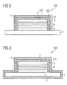
- FIG. 2 An exemplary embodiment of an optoelectronic component 200 is shown.
- the optoelectronic component 200 has an encapsulation arrangement 10, which has a barrier layer 6 on the second electrode 4. On the barrier layer 6, which is applied to the second electrode 4 by means of a first process substep B1 ', a wavelength conversion layer 5 is applied by means of a second process substep B2'.
- the encapsulation assembly 10 may further include a panarization layer (not shown) between the second electrode 4 and the barrier layer 6.
- FIG. 3 an exemplary embodiment of an optoelectronic component 300 is shown, in which the encapsulation arrangement 10 as in the optoelectronic component 100 of FIGS. 1A to 1C has a barrier layer 6 on the wavelength conversion layer 5.
- the barrier layer 6 additionally encloses the substrate 1, so that through the barrier layer 6 and thus through the encapsulation arrangement 10, the substrate 1 together with the electrodes 2, 4 and the radiation-emitting Layer sequence 3 is encapsulated.
- the encapsulation arrangement 10 can for this purpose have further layers on the substrate, such as planarization layers or further barrier layer (not shown).
- FIGS. 4 to 7 show sections of optoelectronic components according to further embodiments.
- an optoelectronic component 400 with an encapsulation arrangement 10 with a layer stack is shown, which has a first barrier layer 61 on the second electrode 4.
- a wavelength conversion layer 5 is applied, on which a second barrier layer 62 is arranged.
- the first barrier layer 61 and the second barrier layer 62 are thus separated from each other by the wavelength conversion layer 5.
- microchannels which can occur, for example, in the first barrier layer 61 and which can represent permeation paths for oxygen and / or moisture, can not continue during the subsequent growth of the second barrier layer 62, since the first and second barrier layers 61, 62 are separated from each other by the wavelength conversion layer 5.
- an improvement in the encapsulation effect can be achieved by a reduction in the permeability of the encapsulation arrangement 10, as a result of which, for example, a smaller overall thickness of the barrier layer 61 and 62 can be possible in comparison to the barrier layers 6 of the preceding embodiments.
- an embodiment for an optoelectronic component 500 which has an encapsulation arrangement 10 with a first wavelength conversion layer 51 on the second electrode 4 having.
- a first barrier layer 6 is applied and on this a second wavelength conversion layer 52 is arranged.
- the two wavelength conversion layers 51, 52 may be the same or different from each other.
- FIG. 6 an embodiment of an optoelectronic device 600 is shown, which combines the advantages of the two preceding embodiments.
- the encapsulation arrangement 10 of the optoelectronic component 600 has a layer stack comprising a plurality of barrier layers 61, 62, 63 and a plurality of wavelength conversion layers 51, 52, which are arranged alternately one above the other.
- the respective numbers of the barrier layers and wavelength conversion layers are purely exemplary and may also differ from the exemplary embodiment shown.
- the thickness of the individual barrier layers 61, 62, 63 can be selected, for example, as approximately one quarter of the characteristic wavelength of the primary radiation or of the secondary radiation, whereby waveguide effects in the barrier layers and thus in the encapsulation arrangement 10 can be avoided.
- the plurality of wavelength conversion layers 51, 52 the color locus of the optoelectronic component awakened luminous impression are easily optimized.
- the encapsulation arrangement 10 offers an effective encapsulation effect while at the same time increasing the coupling-out efficiency of the radiated electromagnetic radiation.
- the optoelectronic component 700 of the embodiment in FIG. 7 2 shows a surface structure 70 on the surface of the encapsulation arrangement 10 facing away from the radiation-emitting layer sequence 3, by means of which the coupling-out efficiency for the radiated electromagnetic radiation can be further increased.
- the surface structure 70 is produced in an outer layer 7, which is formed by an additional polymer layer.
- such a surface structure 70 which is embodied in the embodiment shown as microprisms, can also be produced in a barrier layer or a wavelength conversion layer of the preceding exemplary embodiments.
Landscapes
- Chemical & Material Sciences (AREA)
- Inorganic Chemistry (AREA)
- Physics & Mathematics (AREA)
- Optics & Photonics (AREA)
- Electroluminescent Light Sources (AREA)
- Led Devices (AREA)
- Photovoltaic Devices (AREA)
Applications Claiming Priority (3)
| Application Number | Priority Date | Filing Date | Title |
|---|---|---|---|
| DE102007044865 | 2007-09-20 | ||
| DE102007052181A DE102007052181A1 (de) | 2007-09-20 | 2007-10-31 | Optoelektronisches Bauelement und Verfahren zur Herstellung eines optoelektronischen Bauelements |
| EP08164593.9A EP2040316B1 (fr) | 2007-09-20 | 2008-09-18 | Composant optoélectronique et procédé de fabrication d'un composant optoélectronique |
Related Parent Applications (2)
| Application Number | Title | Priority Date | Filing Date |
|---|---|---|---|
| EP08164593.9 Division | 2008-09-18 | ||
| EP08164593.9A Division-Into EP2040316B1 (fr) | 2007-09-20 | 2008-09-18 | Composant optoélectronique et procédé de fabrication d'un composant optoélectronique |
Publications (2)
| Publication Number | Publication Date |
|---|---|
| EP2429009A2 true EP2429009A2 (fr) | 2012-03-14 |
| EP2429009A3 EP2429009A3 (fr) | 2012-11-21 |
Family
ID=40384462
Family Applications (1)
| Application Number | Title | Priority Date | Filing Date |
|---|---|---|---|
| EP11183323A Withdrawn EP2429009A3 (fr) | 2007-09-20 | 2008-09-18 | Composant optoélectronique et procédé de fabrication d'un composant optoélectronique |
Country Status (4)
| Country | Link |
|---|---|
| US (1) | US20090091258A1 (fr) |
| EP (1) | EP2429009A3 (fr) |
| JP (1) | JP2009076911A (fr) |
| DE (1) | DE102007052181A1 (fr) |
Families Citing this family (34)
| Publication number | Priority date | Publication date | Assignee | Title |
|---|---|---|---|---|
| US9142740B2 (en) * | 2003-07-04 | 2015-09-22 | Epistar Corporation | Optoelectronic element and manufacturing method thereof |
| DE102007044597A1 (de) | 2007-09-19 | 2009-04-02 | Osram Opto Semiconductors Gmbh | Optoelektronisches Bauteil |
| US7955875B2 (en) * | 2008-09-26 | 2011-06-07 | Cree, Inc. | Forming light emitting devices including custom wavelength conversion structures |
| DE102008057720B4 (de) * | 2008-11-17 | 2024-10-31 | OSRAM Opto Semiconductors Gesellschaft mit beschränkter Haftung | Strahlungsemittierende Vorrichtung |
| KR100969100B1 (ko) * | 2010-02-12 | 2010-07-09 | 엘지이노텍 주식회사 | 발광소자, 발광소자의 제조방법 및 발광소자 패키지 |
| US8507872B2 (en) | 2010-03-23 | 2013-08-13 | Nova Scientific, Inc. | Neutron detection |
| DE102010044738A1 (de) * | 2010-09-08 | 2012-03-08 | Osram Opto Semiconductors Gmbh | Dünnschichtverkapselung, optoelektronischer Halbleiterkörper mit einer Dünnschichtverkapselung und Verfahren zur Herstellung einer Dünnschichtverkapselung |
| DE102010051286A1 (de) | 2010-11-12 | 2012-05-16 | Osram Opto Semiconductors Gmbh | Optoelektronischer Halbleiterchip und Verfahren zu dessen Herstellung |
| KR102138213B1 (ko) * | 2010-11-24 | 2020-07-27 | 가부시키가이샤 한도오따이 에네루기 켄큐쇼 | 유기 광 디바이스 및 유기 광 디바이스의 보호 부재 |
| DE102011012298A1 (de) | 2010-12-28 | 2012-06-28 | Osram Opto Semiconductors Gmbh | Verbundsubstrat, Halbleiterchip mit Verbundsubstrat und Verfahren zur Herstellung von Verbundsubstraten und Halbleiterchips |
| US9941438B2 (en) | 2011-03-23 | 2018-04-10 | Nova Scientific, Inc. | Neutron detection |
| DE102011016935A1 (de) * | 2011-04-13 | 2012-10-18 | Osram Opto Semiconductors Gmbh | Verfahren zur Herstellung eines Licht emittierenden Halbleiterbauelements und Licht emittierendes Halbleiterbauelement |
| KR101210180B1 (ko) * | 2011-04-21 | 2012-12-07 | 엘지이노텍 주식회사 | 광학 부재 및 이의 제조방법 |
| US9172057B2 (en) * | 2011-06-30 | 2015-10-27 | Osram Oled Gmbh | Encapsulation structure for an opto-electronic component |
| WO2013106312A2 (fr) * | 2012-01-10 | 2013-07-18 | Ppg Industries Ohio, Inc. | Verres revêtus à faible résistance de couche, à surface lisse et/ou à faible émissivité thermique |
| DE102012203466B4 (de) * | 2012-03-06 | 2021-10-28 | Pictiva Displays International Limited | Organisches licht emittierendes bauelement |
| KR101927055B1 (ko) * | 2012-05-09 | 2018-12-11 | 삼성디스플레이 주식회사 | 광학 시트의 제조 방법, 광학 시트를 구비하는 유기 발광 표시 장치 및 광학 시트를 구비하는 유기 발광 표시 장치의 제조 방법 |
| CN102832356B (zh) * | 2012-08-30 | 2015-04-08 | 京东方科技集团股份有限公司 | Oled封装结构及其制造方法、发光器件 |
| US10147906B2 (en) * | 2014-02-06 | 2018-12-04 | Emagin Corporation | High efficacy seal for organic light emitting diode displays |
| DE102014107167B4 (de) * | 2014-05-21 | 2022-04-21 | OSRAM Opto Semiconductors Gesellschaft mit beschränkter Haftung | Verfahren zur Herstellung eines Halbleiterbauelements mit einer Strukturschicht mit einer Mehrzahl von dreidimensionalen Strukturelementen und strahlungsemittierendes Halbleiterbauelement mit einer Strukturschicht mit einer Mehrzahl von dreidimensionalen Strukturelementen |
| US10622522B2 (en) * | 2014-09-05 | 2020-04-14 | Theodore Lowes | LED packages with chips having insulated surfaces |
| DE102014222920A1 (de) | 2014-11-11 | 2016-05-12 | Osram Oled Gmbh | Licht emittierendes Bauelement und Verfahren zur Herstellung eines Licht emittierenden Bauelements |
| DE102014117764A1 (de) * | 2014-12-03 | 2016-06-09 | Osram Opto Semiconductors Gmbh | Strahlungsemittierendes optoelektronisches Halbleiterbauteil und Verfahren zu dessen Herstellung |
| DE102014117983A1 (de) * | 2014-12-05 | 2016-06-09 | Osram Opto Semiconductors Gmbh | Konversionselement, optoelektronisches Halbleiterbauelement und Verfahren zur Herstellung von Konversionselementen |
| KR102444177B1 (ko) | 2015-12-28 | 2022-09-19 | 삼성디스플레이 주식회사 | 유기 발광 표시 장치 및 이의 제조 방법 |
| KR102651060B1 (ko) * | 2016-08-11 | 2024-03-26 | 삼성디스플레이 주식회사 | 유기 발광 표시 장치 |
| WO2018059702A1 (fr) * | 2016-09-29 | 2018-04-05 | Osram Opto Semiconductors Gmbh | Procédé de fabrication d'un système, système et composant optoélectronique |
| KR102120739B1 (ko) * | 2016-11-07 | 2020-06-09 | 후지필름 가부시키가이샤 | 형광체 함유 필름 및 백라이트 유닛 |
| DE102017101729A1 (de) * | 2017-01-30 | 2018-08-02 | Osram Opto Semiconductors Gmbh | Strahlungsemittierende Vorrichtung |
| KR102533078B1 (ko) * | 2017-06-16 | 2023-05-16 | 삼성디스플레이 주식회사 | 광학 부재 및 이를 포함하는 표시 장치 |
| CN109148709B (zh) * | 2018-09-04 | 2020-09-22 | 合肥鑫晟光电科技有限公司 | 一种电致发光显示面板及显示装置 |
| CN112397629A (zh) * | 2019-08-12 | 2021-02-23 | 深圳光峰科技股份有限公司 | 发光件、显示面板和显示装置 |
| KR20210079898A (ko) * | 2019-12-20 | 2021-06-30 | 엘지디스플레이 주식회사 | 표시장치 |
| US20230087120A1 (en) * | 2021-09-20 | 2023-03-23 | Osram Opto Semiconductiors Gmbh | Method for Producing a Structured Wavelength Conversion Layer and Optoelectronic Device with a Structured Wavelength Conversion Layer |
Citations (1)
| Publication number | Priority date | Publication date | Assignee | Title |
|---|---|---|---|---|
| DE102007049005A1 (de) | 2007-09-11 | 2009-03-12 | Osram Opto Semiconductors Gmbh | Strahlungsemittierende Vorrichtung |
Family Cites Families (37)
| Publication number | Priority date | Publication date | Assignee | Title |
|---|---|---|---|---|
| US5607789A (en) * | 1995-01-23 | 1997-03-04 | Duracell Inc. | Light transparent multilayer moisture barrier for electrochemical cell tester and cell employing same |
| US6712481B2 (en) * | 1995-06-27 | 2004-03-30 | Solid State Opto Limited | Light emitting panel assemblies |
| US6117529A (en) * | 1996-12-18 | 2000-09-12 | Gunther Leising | Organic electroluminescence devices and displays |
| US6252254B1 (en) * | 1998-02-06 | 2001-06-26 | General Electric Company | Light emitting device with phosphor composition |
| DE19853106A1 (de) * | 1998-11-18 | 2000-05-31 | Bayer Ag | Fluoreszierende, strukturierte Formkörper |
| US6566808B1 (en) * | 1999-12-22 | 2003-05-20 | General Electric Company | Luminescent display and method of making |
| CN1389085A (zh) * | 2000-08-23 | 2003-01-01 | 出光兴产株式会社 | 有机el显示装置 |
| WO2002035890A1 (fr) * | 2000-10-25 | 2002-05-02 | Matsushita Electric Industrial Co., Ltd. | Element lumineux, dispositif d'affichage et dispositif d'eclairage mettant cet element en application |
| JP4112800B2 (ja) * | 2000-12-05 | 2008-07-02 | 富士フイルム株式会社 | 発光素子及びその製造方法 |
| WO2002056394A1 (fr) * | 2001-01-09 | 2002-07-18 | Emcore Corporation | Structures d'electrodes pour semi-conducteurs de type p a base de nitrure et leurs procedes de fabrication |
| US6703780B2 (en) * | 2001-01-16 | 2004-03-09 | General Electric Company | Organic electroluminescent device with a ceramic output coupler and method of making the same |
| US6624568B2 (en) * | 2001-03-28 | 2003-09-23 | Universal Display Corporation | Multilayer barrier region containing moisture- and oxygen-absorbing material for optoelectronic devices |
| US6737753B2 (en) * | 2001-09-28 | 2004-05-18 | Osram Opto Semiconductor Gmbh | Barrier stack |
| US6903505B2 (en) * | 2001-12-17 | 2005-06-07 | General Electric Company | Light-emitting device with organic electroluminescent material and photoluminescent materials |
| EP1476000A1 (fr) * | 2002-02-12 | 2004-11-10 | Idemitsu Kosan Co., Ltd. | Ecran electroluminescent et son procede de fabrication |
| EP1492387A1 (fr) * | 2002-03-29 | 2004-12-29 | Pioneer Corporation | Ecran d'affichage organique electroluminescent |
| US7224116B2 (en) * | 2002-09-11 | 2007-05-29 | Osram Opto Semiconductors Gmbh | Encapsulation of active electronic devices |
| JP2004200141A (ja) * | 2002-10-24 | 2004-07-15 | Toyota Industries Corp | 有機el素子 |
| US6717176B1 (en) * | 2002-11-12 | 2004-04-06 | Opto Tech Corporation | White light emitting organic electro-luminescent device and method for fabricating the same |
| US7011983B2 (en) * | 2002-12-20 | 2006-03-14 | General Electric Company | Large organic devices and methods of fabricating large organic devices |
| JP2004220874A (ja) * | 2003-01-14 | 2004-08-05 | Tohoku Pioneer Corp | 有機el素子、およびその製造方法 |
| JP3717480B2 (ja) * | 2003-01-27 | 2005-11-16 | ローム株式会社 | 半導体発光装置 |
| US6847162B2 (en) * | 2003-04-29 | 2005-01-25 | General Electric Company | Light source with organic layer and photoluminescent layer |
| JP2005063926A (ja) * | 2003-06-27 | 2005-03-10 | Toyota Industries Corp | 発光デバイス |
| US20070201234A1 (en) * | 2003-07-21 | 2007-08-30 | Clemens Ottermann | Luminous element |
| JP4195352B2 (ja) * | 2003-09-10 | 2008-12-10 | 三星エスディアイ株式会社 | 発光素子基板およびそれを用いた発光素子 |
| US20050173724A1 (en) * | 2004-02-11 | 2005-08-11 | Heng Liu | Group III-nitride based LED having a transparent current spreading layer |
| US7230374B2 (en) * | 2003-09-22 | 2007-06-12 | Samsung Sdi Co., Ltd. | Full color organic light-emitting device having color modulation layer |
| JP4538784B2 (ja) * | 2003-10-07 | 2010-09-08 | 富士電機ホールディングス株式会社 | 色変換フィルタの製造方法および装置 |
| JP4590905B2 (ja) * | 2003-10-31 | 2010-12-01 | 豊田合成株式会社 | 発光素子および発光装置 |
| WO2005074330A1 (fr) * | 2004-01-28 | 2005-08-11 | Agency For Science, Technology And Research | Dispositifs electroluminescents organiques multicolores |
| US7250715B2 (en) * | 2004-02-23 | 2007-07-31 | Philips Lumileds Lighting Company, Llc | Wavelength converted semiconductor light emitting devices |
| JP2006156968A (ja) * | 2004-10-26 | 2006-06-15 | Doshisha Co Ltd | 発光素子 |
| US7344902B2 (en) * | 2004-11-15 | 2008-03-18 | Philips Lumileds Lighting Company, Llc | Overmolded lens over LED die |
| KR100635575B1 (ko) * | 2004-11-17 | 2006-10-17 | 삼성에스디아이 주식회사 | 풀 칼라 유기 전계 발광 표시 소자 및 그 제조방법 |
| JP2006313829A (ja) * | 2005-05-09 | 2006-11-16 | Konica Minolta Opto Inc | 白色発光ダイオード及びその製造方法 |
| US20070054149A1 (en) * | 2005-08-23 | 2007-03-08 | Chi-Ming Cheng | Substrate assembly of a display device and method of manufacturing the same |
-
2007
- 2007-10-31 DE DE102007052181A patent/DE102007052181A1/de not_active Withdrawn
-
2008
- 2008-09-18 JP JP2008239744A patent/JP2009076911A/ja active Pending
- 2008-09-18 EP EP11183323A patent/EP2429009A3/fr not_active Withdrawn
- 2008-09-22 US US12/235,121 patent/US20090091258A1/en not_active Abandoned
Patent Citations (1)
| Publication number | Priority date | Publication date | Assignee | Title |
|---|---|---|---|---|
| DE102007049005A1 (de) | 2007-09-11 | 2009-03-12 | Osram Opto Semiconductors Gmbh | Strahlungsemittierende Vorrichtung |
Also Published As
| Publication number | Publication date |
|---|---|
| DE102007052181A1 (de) | 2009-04-02 |
| US20090091258A1 (en) | 2009-04-09 |
| EP2429009A3 (fr) | 2012-11-21 |
| JP2009076911A (ja) | 2009-04-09 |
Similar Documents
| Publication | Publication Date | Title |
|---|---|---|
| DE102007052181A1 (de) | Optoelektronisches Bauelement und Verfahren zur Herstellung eines optoelektronischen Bauelements | |
| DE102007053286B4 (de) | Verfahren zur Herstellung eines optoelektronischen Bauelements | |
| EP1906462B1 (fr) | Composant optoélectronique doté d'une couche de conversion luminescente | |
| DE102011114641B4 (de) | Optoelektronisches Halbleiterbauelement und Verfahren zur Herstellung eines optoelektronischen Halbleiterbauelements | |
| EP2020038B1 (fr) | Puce de semi-conducteur optoélectronique munie de trois substances de conversion de longueur d'onde, composant semi-conducteur optoélectronique muni d'une telle puce et procédé de fabrication de cette puce de semi-conducteur optoélectronique | |
| EP2238634B1 (fr) | Procédé pour produire un composant électronique | |
| KR100872281B1 (ko) | 나노와이어 구조체를 이용한 반도체 발광소자 및 그제조방법 | |
| EP2193561B1 (fr) | Composant optoélectronique | |
| EP2258000B1 (fr) | Composant semiconducteur optoélectronique et procédé de fabrication d'un composant semiconducteur optoélectronique | |
| EP2054948A1 (fr) | Composant optoélectronique | |
| DE102007032280A1 (de) | Optoelektronisches Bauelement | |
| EP0854662A2 (fr) | Panneau d'affichage électroluminescent à couleurs | |
| DE102008020816A1 (de) | Organische Leuchtdiode, Kontaktanordnung und Verfahren zur Herstellung einer organischen Leuchtdiode | |
| DE102008012407A1 (de) | Strahlungsemittierende Vorrichtung | |
| EP2201624A1 (fr) | Composant optoélectronique | |
| DE102015113052A1 (de) | Optoelektronisches Bauelement umfassend ein Konversionselement, Verfahren zur Herstellung eines optoelektronischen Bauelements umfassend ein Konversionselement und Verwendung eines optoelektronischen Bauelements umfassend ein Konversionselement | |
| DE102015105484B4 (de) | Organisches Licht emittierendes Bauelement | |
| EP2040316B1 (fr) | Composant optoélectronique et procédé de fabrication d'un composant optoélectronique | |
| DE102016119539A1 (de) | Licht emittierender Halbleiterchip und Licht emittierende Vorrichtung | |
| WO2014048905A1 (fr) | Composant optoélectronique à semi-conducteurs | |
| DE102006045702A1 (de) | Optoelektronisches Bauteil | |
| DE102015100253B4 (de) | Licht emittierende Vorrichtung | |
| DE102013106992A1 (de) | Optoelektronisches Bauelement, Verfahren zum Herstellen eines optoelektronischen Bauelementes | |
| DE102018128167B4 (de) | OLED-Tafel für Beleuchtungsvorrichtung und Verfahren zu ihrer Herstellung | |
| DE102008018353A1 (de) | Strahlungsemittierendes optoelektronisches Bauelement und Verfahren zur Herstellung eines strahlungsemittierenden Bauelelements |
Legal Events
| Date | Code | Title | Description |
|---|---|---|---|
| 17P | Request for examination filed |
Effective date: 20110929 |
|
| AC | Divisional application: reference to earlier application |
Ref document number: 2040316 Country of ref document: EP Kind code of ref document: P |
|
| AK | Designated contracting states |
Kind code of ref document: A2 Designated state(s): DE FR GB |
|
| PUAI | Public reference made under article 153(3) epc to a published international application that has entered the european phase |
Free format text: ORIGINAL CODE: 0009012 |
|
| PUAL | Search report despatched |
Free format text: ORIGINAL CODE: 0009013 |
|
| AK | Designated contracting states |
Kind code of ref document: A3 Designated state(s): DE FR GB |
|
| RIC1 | Information provided on ipc code assigned before grant |
Ipc: H01L 33/50 20100101ALI20121015BHEP Ipc: H01L 51/52 20060101AFI20121015BHEP Ipc: H01L 33/52 20100101ALI20121015BHEP |
|
| RAP1 | Party data changed (applicant data changed or rights of an application transferred) |
Owner name: OSRAM OLED GMBH |
|
| GRAP | Despatch of communication of intention to grant a patent |
Free format text: ORIGINAL CODE: EPIDOSNIGR1 |
|
| RIC1 | Information provided on ipc code assigned before grant |
Ipc: H01L 33/50 20100101ALI20180614BHEP Ipc: H01L 51/52 20060101AFI20180614BHEP Ipc: H01L 33/52 20100101ALI20180614BHEP |
|
| INTG | Intention to grant announced |
Effective date: 20180706 |
|
| STAA | Information on the status of an ep patent application or granted ep patent |
Free format text: STATUS: THE APPLICATION IS DEEMED TO BE WITHDRAWN |
|
| 18D | Application deemed to be withdrawn |
Effective date: 20181117 |