EP2432040A2 - Organische lichtemittierende diode und verfahren zu ihrer herstellung - Google Patents
Organische lichtemittierende diode und verfahren zu ihrer herstellung Download PDFInfo
- Publication number
- EP2432040A2 EP2432040A2 EP10775055A EP10775055A EP2432040A2 EP 2432040 A2 EP2432040 A2 EP 2432040A2 EP 10775055 A EP10775055 A EP 10775055A EP 10775055 A EP10775055 A EP 10775055A EP 2432040 A2 EP2432040 A2 EP 2432040A2
- Authority
- EP
- European Patent Office
- Prior art keywords
- electrode
- layer
- group
- set forth
- transparent layer
- Prior art date
- Legal status (The legal status is an assumption and is not a legal conclusion. Google has not performed a legal analysis and makes no representation as to the accuracy of the status listed.)
- Withdrawn
Links
Images


Classifications
-
- H—ELECTRICITY
- H10—SEMICONDUCTOR DEVICES; ELECTRIC SOLID-STATE DEVICES NOT OTHERWISE PROVIDED FOR
- H10K—ORGANIC ELECTRIC SOLID-STATE DEVICES
- H10K50/00—Organic light-emitting devices
- H10K50/80—Constructional details
- H10K50/805—Electrodes
- H10K50/82—Cathodes
- H10K50/828—Transparent cathodes, e.g. comprising thin metal layers
-
- H—ELECTRICITY
- H05—ELECTRIC TECHNIQUES NOT OTHERWISE PROVIDED FOR
- H05B—ELECTRIC HEATING; ELECTRIC LIGHT SOURCES NOT OTHERWISE PROVIDED FOR; CIRCUIT ARRANGEMENTS FOR ELECTRIC LIGHT SOURCES, IN GENERAL
- H05B33/00—Electroluminescent light sources
- H05B33/10—Apparatus or processes specially adapted to the manufacture of electroluminescent light sources
-
- H—ELECTRICITY
- H05—ELECTRIC TECHNIQUES NOT OTHERWISE PROVIDED FOR
- H05B—ELECTRIC HEATING; ELECTRIC LIGHT SOURCES NOT OTHERWISE PROVIDED FOR; CIRCUIT ARRANGEMENTS FOR ELECTRIC LIGHT SOURCES, IN GENERAL
- H05B33/00—Electroluminescent light sources
- H05B33/12—Light sources with substantially two-dimensional [2D] radiating surfaces
- H05B33/22—Light sources with substantially two-dimensional [2D] radiating surfaces characterised by the chemical or physical composition or the arrangement of auxiliary dielectric or reflective layers
-
- H—ELECTRICITY
- H10—SEMICONDUCTOR DEVICES; ELECTRIC SOLID-STATE DEVICES NOT OTHERWISE PROVIDED FOR
- H10K—ORGANIC ELECTRIC SOLID-STATE DEVICES
- H10K50/00—Organic light-emitting devices
- H10K50/80—Constructional details
- H10K50/85—Arrangements for extracting light from the devices
- H10K50/858—Arrangements for extracting light from the devices comprising refractive means, e.g. lenses
-
- H—ELECTRICITY
- H10—SEMICONDUCTOR DEVICES; ELECTRIC SOLID-STATE DEVICES NOT OTHERWISE PROVIDED FOR
- H10K—ORGANIC ELECTRIC SOLID-STATE DEVICES
- H10K71/00—Manufacture or treatment specially adapted for the organic devices covered by this subclass
-
- H—ELECTRICITY
- H10—SEMICONDUCTOR DEVICES; ELECTRIC SOLID-STATE DEVICES NOT OTHERWISE PROVIDED FOR
- H10K—ORGANIC ELECTRIC SOLID-STATE DEVICES
- H10K2102/00—Constructional details relating to the organic devices covered by this subclass
- H10K2102/10—Transparent electrodes, e.g. using graphene
- H10K2102/101—Transparent electrodes, e.g. using graphene comprising transparent conductive oxides [TCO]
- H10K2102/102—Transparent electrodes, e.g. using graphene comprising transparent conductive oxides [TCO] comprising tin oxides, e.g. fluorine-doped SnO2
-
- H—ELECTRICITY
- H10—SEMICONDUCTOR DEVICES; ELECTRIC SOLID-STATE DEVICES NOT OTHERWISE PROVIDED FOR
- H10K—ORGANIC ELECTRIC SOLID-STATE DEVICES
- H10K2102/00—Constructional details relating to the organic devices covered by this subclass
- H10K2102/10—Transparent electrodes, e.g. using graphene
- H10K2102/101—Transparent electrodes, e.g. using graphene comprising transparent conductive oxides [TCO]
- H10K2102/103—Transparent electrodes, e.g. using graphene comprising transparent conductive oxides [TCO] comprising indium oxides, e.g. ITO
-
- H—ELECTRICITY
- H10—SEMICONDUCTOR DEVICES; ELECTRIC SOLID-STATE DEVICES NOT OTHERWISE PROVIDED FOR
- H10K—ORGANIC ELECTRIC SOLID-STATE DEVICES
- H10K2102/00—Constructional details relating to the organic devices covered by this subclass
- H10K2102/301—Details of OLEDs
- H10K2102/302—Details of OLEDs of OLED structures
- H10K2102/3023—Direction of light emission
- H10K2102/3031—Two-side emission, e.g. transparent OLEDs [TOLED]
Definitions
- the present invention relates to an organic light emitting diode, and more particularly to an organic light emitting diode in which the light transmittance of a transparent cathode is improved, and to a method of manufacturing the same.
- an organic light emitting diode includes a substrate, a bottom electrode formed on the substrate, an organic layer formed on the bottom electrode and a top electrode formed on the organic layer.
- the OLED emits light using electrical conduction between an anode used as the bottom electrode and a cathode used as the top electrode. Specifically, the light emission of the OLED occurs at the organic layer disposed between the top electrode and the bottom electrode by means of electrons of the top electrode and holes of the bottom electrode.
- OLEDs are classified into, depending on the light emission manner, transparent OLEDs which emit light through a top electrode and a bottom electrode, top OLEDs that emit light through a top electrode, and bottom OLEDs that emit light through a bottom electrode.
- the light emission manner of the OLED is achieved by either or both of the electrodes that are transparent among the top electrode and the bottom electrode.
- both the top electrode and the bottom electrode must be transparent.
- the bottom electrode may be a transparent indium-tin-oxide (ITO) electrode
- the top electrode may be a transparent metal film. As such, when the thickness of such a metal film is reduced, transmittance may be increased.
- ITO indium-tin-oxide
- the sheet resistance of the top electrode may increase. Specifically, as the thickness of the top electrode is reduced in order to increase the transmittance thereof, resistance thereof increases, undesirably deteriorating total performance of the OLED.
- the present invention has been made keeping in mind the problems encountered in the related art and the present invention is intended to provide an OLED, which is able to increase the transmittance of a cathode.
- the present invention is intended to provide an OLED, which is efficiently configured such that resistance of a cathode is prevented from increasing in proportion to the increase in transmittance thereof.
- the present invention is intended to provide a method of manufacturing the OLED.
- An aspect of the present invention provides an OLED, including a substrate, a first electrode formed on the substrate, an organic layer formed on the first electrode, a second electrode formed on the organic layer, and a transparent layer formed at either one or both of a position between the organic layer and the second electrode and a position on the upper surface of the second electrode and including any one selected from the group consisting of an oxide, a nitride, a salt and mixtures thereof.
- the oxide may include any one selected from the group consisting of MoO 3 , ITO, IZO, IO, ZnO, TO, TiO 2 , SiO 2 , WO 3 , Al 2 O 3 , Cr 2 O 3 , TeO 2 , and SrO 2 .
- the nitride may include any one selected from the group consisting of Si 3 N 4 and AlN.
- the salt may include any one selected from the group consisting of Cs 2 CO 3 , Li 2 CO 3 , K 2 CO 3 , Na 2 CO 3 , LiF, CsF, and ZnSe.
- the transparent layer may have a thickness ranging from 0.1 nm to less than 100 nm.
- the organic layer may include an electron transporting layer formed by doping any one selected from the group consisting of a metal having low work function and a compound thereof, in order to facilitate the injection of electrons from the second electrode.
- the metal having low work function may include any one selected from the group consisting of Cs, Li, Na, K, and Ca.
- the compound thereof may include any one selected from the group consisting of Li-Al, LiF, CsF, and Cs 2 CO 3 .
- the OLED may exhibit a transmittance of 70 - 99% depending on a wavelength (nm).
- Another aspect of the present invention provides a method of manufacturing an OLED, including forming a first electrode on a substrate, forming an organic layer on the first electrode, forming a second electrode on the organic layer, and forming a transparent layer including any one selected from the group consisting of an oxide, a nitride, a salt and mixtures thereof at either one or both of a position between the organic layer and the second electrode and a position on the upper surface of the second electrode.
- the OLED is configured such that a transparent layer including any one selected from among an oxide, a nitride, a salt and mixtures thereof is formed at either one or both of a position between an organic layer and a second electrode (cathode) and a position on the upper surface of the second electrode, thereby achieving double-sided light emission and increasing transmittance.
- the transparent layer is formed of any one selected from among an oxide, a nitride, a salt and mixtures thereof, the internal resistance of the second electrode can be prevented from increasing, thus improving electrical performance of products.
- the OLED 1 may include a substrate 10, a first electrode 30, a second electrode 50, an organic layer 70, and a transparent layer 90.
- the substrate 10 supports the first electrode 30, the second electrode 50, the organic layer 70 and the transparent layer 90.
- the substrate 10 may be formed of a glass material or a plastic material, which is transparent so as to permit emitted light to pass therethrough.
- the first electrode 30 is typically referred to as a bottom electrode, and is formed on the substrate 10.
- the first electrode 30 is an anode which is a positive electrode and is formed on the substrate 10 using sputtering, ion plating or thermal evaporation using an e-gun.
- the first electrode 30 may be a transparent ITO electrode, or alternatively may be a transparent indium-zinc-oxide electrode.
- the second electrode 50 is typically referred to as a top electrode disposed to face the first electrode 30, and is formed on the organic layer 70.
- the second electrode 50 is a cathode which is a negative electrode oppositely charged to the first electrode 30 which is the positive electrode.
- the second electrode 50 may be formed of any one selected from among silver (Ag), aluminum (Al) and a magnesium-silver (Mg-Ag) alloy, so that it is transparent.
- the organic layer 70 is disposed between the first electrode 30 and the second electrode 50, and emits light using electrical conduction between the first electrode 30 and the second electrode 50.
- the organic layer 70 includes a hole injection layer (HIL) 72, a hole transporting layer (HTL) 74, an emissive layer (EML) 76, an electron transporting layer (ETL) 78 and an electron injection layer (EIL) 79, in order to emit light using electrical conduction between the first electrode 30 and the second electrode 50.
- HIL hole injection layer
- HTL hole transporting layer
- EML emissive layer
- ETL electron transporting layer
- EIL electron injection layer
- the organic layer 70 may be formed between the first electrode 30 and the second electrode 50 using spin coating, thermal evaporation, spin casting, sputtering, e-beam evaporation or chemical vapor deposition (CVD).
- spin coating thermal evaporation, spin casting, sputtering, e-beam evaporation or chemical vapor deposition (CVD).
- the hole injection layer 72 functions to inject holes from the first electrode 30, and the hole transporting layer 74 functions to transport the holes injected from the hole injection layer 72 so as to meet with electrons of the second electrode 50.
- the electron injection layer 79 functions to inject electrons from the second electrode 50
- the electron transporting layer 78 functions to transport the electrons injected from the electron injection layer 79 so as to meet with the holes transported from the hole transporting layer 74 at the emissive layer 76.
- the electron transporting layer 78 may be formed by doping any one selected from among a metal having low work function and a compound thereof, in order to facilitate the injection of the electrons from the second electrode 50, and may be applied regardless of whether the electron injection layer 79 is provided or not.
- examples of the metal having low work function may include Cs, Li, Na, K, and Ca, and examples of the compound thereof may include Li-Al, LiF, CsF, and Cs 2 CO 3 .
- the emissive layer 76 is disposed between the hole transporting layer 74 and the electron transporting layer 78 and thus emits light by means of the holes from the hole transporting layer 74 and the electrons from the electron transporting layer 78. Specifically, light emission takes place by virtue of the holes and the electrons which meet and recombine with each other in the emissive layer 76, that is, at the interfaces between the hole transporting layer 74 and the electron transporting layer 78.
- the transparent layer 90 may be formed at either one or both of a position between the organic layer 70 and the second electrode 50 and a position on the upper surface of the second electrode 50.
- the transparent layer 90 may be formed on both the upper surface and the lower surface of the second electrode 50, or alternatively only on either of the lower surface and the upper surface of the second electrode 50.
- the configuration in which the transparent layer 90 is formed on both of the upper and lower surfaces of the second electrode 50 is illustrated.
- the present invention is not limited thereto, and it goes without saying that the configuration in which the transparent layer is formed only on either of the lower and upper surfaces of the second electrode 50 be able to be applied as well.
- the transparent layer 90 may include a first transparent layer 91 formed between the organic layer 70 and the second electrode 50, and a second transparent layer 92 formed on the upper surface of the second electrode 50.
- the first transparent layer 91 may be formed between the electron injection layer 79 of the organic layer 70 and the second electrode 50, or may be formed in the electron injection layer 79 itself.
- the second transparent layer 92 may be formed on the upper surface of the second electrode 50 opposite the surface on which the first transparent layer 91 is formed.
- the transparent layer 90 plays a role in imparting the second electrode 50 with transparency and high transmittance.
- the transparent layer 90 is provided in the form of a thin film to thus reduce the sheet resistance of the second electrode 50, thereby preventing the performance of the OLED 1 from deteriorating.
- the properties of the transparent layer 90 are specified with reference to FIGS. 2 to 4 after the following description of an oxide, a nitride, a salt and mixtures thereof is given.
- the transparent layer 90 according to the present invention may include any one selected from among an oxide, a nitride, a salt and mixtures thereof.
- Examples of the oxide may include MoO 3 , ITO, IZO, IO, ZnO, TO, TiO 2 , SiO 2 , WO 3 , Al 2 O 3 , Cr 2 O 3 , TeO 2 , and SrO 2
- examples of the nitride may include Si 3 N 4 , and A1N.
- examples of the salt may include Cs 2 CO 3 , Li 2 CO 3 , K 2 CO 3 , Na 2 CO 3 , LiF, CsF, and ZnSe.
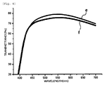
- the transparent layer 90 When the transparent layer 90 is formed using an oxide, a nitride, a salt or a mixture thereof, it preferably exhibits superior transmittance and luminance as shown in FIGS. 2 to 4 . In addition to the above materials, any material may be used so long as the second electrode 50 is transparent and has high transmittance.
- the first transparent layer 91 and the second transparent layer 92 may be formed of the same material, or alternatively may be formed of different materials.
- the first transparent layer 91 may include an oxide
- the second transparent layer 92 may include a nitride, a salt or a mixture thereof.
- the first transparent layer 91 may include a nitride
- the second transparent layer 92 may include an oxide, a salt or a mixture thereof.
- the first transparent layer 91 may include a salt
- the second transparent layer 92 may include an oxide, a nitride or a mixture thereof.
- the thickness of the transparent layer 90 may be set in the range from 0.1 nm to less than 100 nm. The reason why the thickness of the transparent layer 90 is limited is that if the thickness of the transparent layer 90 is less than 0.1 nm, transmittance is increased but resistance may also increase proportionally thereto, undesirably deteriorating the performance of the OLED 1.
- the transparent layer 90 may be formed using thermal evaporation.
- FIG. 2 is a graph showing the transmittance of the OLED 1 depending on whether the transparent layer 90 is provided or not.
- curve “a” depicts the transmittance of the OLED 1 with the transparent layer 90 according to the present invention
- curve “b” depicts the transmittance of the OLED 1 without the transparent layer 90, unlike the present invention.
- the OLED 1 according to the present invention may exhibit a transmittance of 70 - 99% depending on a wavelength (nm).
- the OLED 1 according to the present invention may show a transmittance of about 80% at 550 nm, and the OLED 1 without the transparent layer 90 may show a transmittance of about 47% at 550 nm.
- the transmittance of the OLED 1 with the transparent layer 90 can be seen to be 1.7 times higher than that of the OLED 1 without the transparent layer 90.
- FIG. 3 is a graph showing the luminance of the OLED 1 depending on whether the transparent layer 90 is provided or not.
- curve “c" depicts the luminance of the OLED 1 with the transparent layer 90 according to the present invention
- curve “d” depicts the luminance of the OLED 1 without the transparent layer 90.
- the OLED 1 with the transparent layer 90 manifests a luminance of about 25,000 at a voltage of 10 V, whereas the OLED 1 without the transparent layer 90 shows a luminance of about 20,000 at 10 V. From this, it can be seen that there is a 1.25 times difference in the luminance depending on whether the transparent layer 90 is provided or not.
- curve “e” depicts the transmittance when the transparent layer 90 is formed of an oxide such as MoO 3 , ITO, IZO, IO, ZnO, TO, TiO 2 , SiO 2 , WO 3 , Al 2 O 3 , Cr 2 O 3 , TeO 2 , or SrO 2
- curve "f” depicts the transmittance when the transparent layer 90 is formed of a salt such as Cs 2 CO 3 , Li 2 CO 3 , K 2 CO 3 , Na 2 CO 3 , LiF, CsF, or ZnSe.
- the transmittance is determined to be about 80% when the transparent layer 90 is formed of an oxide, and is determined to be about 75% when the transparent layer 90 is formed of a salt. Although the transmittance is about 5% higher when using the transparent layer 90 formed of an oxide than when using the transparent layer 90 formed of a salt, this is a small difference.
- an oxide, a salt and mixtures thereof may be selectively used as in the embodiment of the present invention.
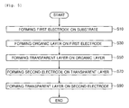
- FIG. 5 a method of manufacturing the OLED 1 according to the present invention is described below.
- a first electrode 30 which is a positive electrode is formed on a substrate 10 (S10).
- an organic layer 70 is formed on the first electrode 30 which has been formed on the substrate 10 (S30).
- the organic layer 70 formed on the first electrode 30 includes a hole injection layer 72, a hole transporting layer 74, an emissive layer 76, an electron transporting layer 78 and an electron injection layer 79, which are sequentially formed.
- the first transparent layer 91 is formed on the organic layer 70 (S50).
- the first transparent layer 91 may include an oxide such as MoO 3 , ITO, IZO, IO, ZnO, TO, TiO 2 , SiO 2 , WO 3 , Al 2 O 3 , Cr 2 O 3 , TeO 2 , or SrO 2 .
- the first transparent layer 91 is formed to a thickness ranging from 0.1 nm to less than 100 nm.
- the second electrode 50 which is a negative electrode may include a metal film.
- the metal film used as the second electrode 50 may include any one selected from among Ag, Al and an Mg-Ag alloy.
- a second transparent layer 92 is formed on the second electrode 50 (S90).
- the second transparent layer 92 may include an oxide as in S50.
- the second transparent layer 92 formed on the second electrode 50 may include a nitride such as Si 3 N 4 or A1N, a salt such as Cs 2 CO 3 , Li 2 CO 3 , K 2 CO 3 , Na 2 CO 3 , LiF, CsF or ZnSe, or a mixture thereof.
- the transparent layer 90 is formed on both surfaces of the second electrode 50 in this way, double-sided light emission is possible and the transmittance may be increased.
- the thickness of the second electrode 50 may be adjusted, thus improving the transmittance and electrical performance.
Landscapes
- Physics & Mathematics (AREA)
- Optics & Photonics (AREA)
- Engineering & Computer Science (AREA)
- Manufacturing & Machinery (AREA)
- Electroluminescent Light Sources (AREA)
Applications Claiming Priority (3)
| Application Number | Priority Date | Filing Date | Title |
|---|---|---|---|
| KR20090041540 | 2009-05-13 | ||
| KR1020090047783A KR101148886B1 (ko) | 2009-05-13 | 2009-05-29 | 유기전계발광소자 및 그 제조방법 |
| PCT/KR2010/002721 WO2010131853A2 (ko) | 2009-05-13 | 2010-04-29 | 유기전계발광소자 및 그 제조방법 |
Publications (2)
| Publication Number | Publication Date |
|---|---|
| EP2432040A2 true EP2432040A2 (de) | 2012-03-21 |
| EP2432040A4 EP2432040A4 (de) | 2013-10-23 |
Family
ID=43407665
Family Applications (2)
| Application Number | Title | Priority Date | Filing Date |
|---|---|---|---|
| EP10775055.6A Withdrawn EP2432040A4 (de) | 2009-05-13 | 2010-04-29 | Organische lichtemittierende diode und verfahren zu ihrer herstellung |
| EP10775056.4A Withdrawn EP2432041A4 (de) | 2009-05-13 | 2010-04-29 | Organische lichtemittierende diode und verfahren zu ihrer herstellung |
Family Applications After (1)
| Application Number | Title | Priority Date | Filing Date |
|---|---|---|---|
| EP10775056.4A Withdrawn EP2432041A4 (de) | 2009-05-13 | 2010-04-29 | Organische lichtemittierende diode und verfahren zu ihrer herstellung |
Country Status (6)
| Country | Link |
|---|---|
| US (2) | US20100289016A1 (de) |
| EP (2) | EP2432040A4 (de) |
| JP (2) | JP2012527083A (de) |
| KR (7) | KR101148886B1 (de) |
| CN (2) | CN102422453A (de) |
| WO (2) | WO2010131853A2 (de) |
Families Citing this family (18)
| Publication number | Priority date | Publication date | Assignee | Title |
|---|---|---|---|---|
| JP2011145344A (ja) | 2010-01-12 | 2011-07-28 | Seiko Epson Corp | 電気光学装置とその駆動方法、及び電子機器 |
| EP2696569A4 (de) * | 2011-04-06 | 2014-07-16 | Neoviewkolon Co Ltd | Bildschirm zur anzeige von informationen für eine optische vorrichtung |
| CN103137878A (zh) * | 2011-11-29 | 2013-06-05 | 海洋王照明科技股份有限公司 | 有机电致发光器件及其制备方法 |
| WO2013187119A1 (ja) * | 2012-06-14 | 2013-12-19 | コニカミノルタ株式会社 | 電界発光素子およびその電界発光素子を用いた照明装置 |
| KR20140040650A (ko) * | 2012-09-24 | 2014-04-03 | 네오뷰코오롱 주식회사 | 유기발광 표시장치 |
| WO2014046514A1 (ko) * | 2012-09-24 | 2014-03-27 | 네오뷰코오롱 주식회사 | 유기발광 표시장치 |
| KR102133451B1 (ko) * | 2013-02-22 | 2020-07-14 | 삼성전자주식회사 | 광전 소자 및 이미지 센서 |
| CN104183715A (zh) * | 2013-05-22 | 2014-12-03 | 海洋王照明科技股份有限公司 | 有机电致发光器件及其制作方法 |
| CN104183760A (zh) * | 2013-05-22 | 2014-12-03 | 海洋王照明科技股份有限公司 | 有机电致发光器件及其制作方法 |
| CN104183753A (zh) * | 2013-05-22 | 2014-12-03 | 海洋王照明科技股份有限公司 | 有机电致发光器件及其制作方法 |
| KR20150019620A (ko) | 2013-08-14 | 2015-02-25 | 삼성디스플레이 주식회사 | 유기발광 표시 장치 |
| KR102232945B1 (ko) * | 2014-07-24 | 2021-03-25 | 엘지디스플레이 주식회사 | 유기 발광 표시 장치 및 유기 발광 표시 장치 제조 방법 |
| KR20160116121A (ko) | 2015-03-25 | 2016-10-07 | 삼성디스플레이 주식회사 | 박막 트랜지스터 표시판 및 이를 포함하는 표시 장치 |
| WO2016182370A1 (ko) * | 2015-05-14 | 2016-11-17 | 서울대학교산학협력단 | 웨어러블 양자점 디스플레이 장치 및 이를 포함하는 웨어러블 전자 장치 |
| CN109360903A (zh) * | 2018-10-31 | 2019-02-19 | 武汉华星光电技术有限公司 | 有机发光二极管显示器及其制造方法 |
| US11239305B2 (en) | 2019-07-24 | 2022-02-01 | Taiwan Semiconductor Manufacturing Company, Ltd. | Display device and manufacturing method thereof |
| CN115997488A (zh) * | 2020-08-20 | 2023-04-21 | 应用材料公司 | Oled光场架构 |
| CN113707821B (zh) * | 2021-07-08 | 2024-10-25 | 上饶小姆软件中心(个人独资) | 用于电子传输层的组合物及其制备方法和应用 |
Family Cites Families (55)
| Publication number | Priority date | Publication date | Assignee | Title |
|---|---|---|---|---|
| JPH10125469A (ja) | 1996-10-24 | 1998-05-15 | Tdk Corp | 有機el発光素子 |
| DE69729394T2 (de) * | 1996-11-29 | 2005-06-02 | Idemitsu Kosan Co. Ltd. | Organische elektrolumineszente Vorrichtung |
| US5739545A (en) | 1997-02-04 | 1998-04-14 | International Business Machines Corporation | Organic light emitting diodes having transparent cathode structures |
| JP3374035B2 (ja) * | 1997-03-21 | 2003-02-04 | 三洋電機株式会社 | 有機エレクトロルミネッセンス素子 |
| US6468676B1 (en) * | 1999-01-02 | 2002-10-22 | Minolta Co., Ltd. | Organic electroluminescent display element, finder screen display device, finder and optical device |
| US6639357B1 (en) * | 2000-02-28 | 2003-10-28 | The Trustees Of Princeton University | High efficiency transparent organic light emitting devices |
| JP2001338755A (ja) * | 2000-03-21 | 2001-12-07 | Seiko Epson Corp | 有機el素子およびその製造方法 |
| KR100822569B1 (ko) * | 2000-09-07 | 2008-04-16 | 이데미쓰 고산 가부시키가이샤 | 유기 전계 발광 소자 |
| EP2226365B1 (de) * | 2001-10-25 | 2016-08-10 | Panasonic Intellectual Property Management Co., Ltd. | Tafellichtemittierender Körper |
| JP2003142262A (ja) * | 2001-11-06 | 2003-05-16 | Seiko Epson Corp | 電気光学装置、膜状部材、積層膜、低屈折率膜、多層積層膜、電子機器 |
| US6833667B2 (en) * | 2002-02-27 | 2004-12-21 | Matsushita Electric Industrial Co., Ltd. | Organic electroluminescence element and image forming apparatus or portable terminal unit using thereof |
| KR100480361B1 (ko) * | 2002-04-18 | 2005-03-30 | 네오뷰코오롱 주식회사 | 박막형 게터층이 형성된 밀봉형 유기 발광 소자 및 그제조방법 |
| JP4165145B2 (ja) * | 2002-08-07 | 2008-10-15 | 株式会社日立製作所 | 有機発光表示装置 |
| JP2004140267A (ja) * | 2002-10-18 | 2004-05-13 | Semiconductor Energy Lab Co Ltd | 半導体装置およびその作製方法 |
| KR100662297B1 (ko) * | 2002-10-18 | 2007-01-02 | 엘지전자 주식회사 | 유기 el 소자 |
| DE10252903A1 (de) * | 2002-11-12 | 2004-05-19 | Philips Intellectual Property & Standards Gmbh | Organische elektrolumineszente Lichtquelle mit Antireflexionsschicht |
| CN102281659B (zh) * | 2002-12-26 | 2014-06-04 | 株式会社半导体能源研究所 | 发光装置和制造发光装置的方法 |
| JP4186688B2 (ja) * | 2003-04-17 | 2008-11-26 | 三菱化学株式会社 | エレクトロルミネッセンス素子 |
| KR100527191B1 (ko) * | 2003-06-03 | 2005-11-08 | 삼성에스디아이 주식회사 | 저저항 캐소드를 사용하는 유기 전계 발광 소자 |
| KR100563058B1 (ko) * | 2003-11-21 | 2006-03-24 | 삼성에스디아이 주식회사 | 유기 전계 발광 소자 |
| GB0401613D0 (en) * | 2004-01-26 | 2004-02-25 | Cambridge Display Tech Ltd | Organic light emitting diode |
| JP4131243B2 (ja) * | 2004-02-06 | 2008-08-13 | セイコーエプソン株式会社 | 電気光学装置の製造方法、電気光学装置、及び電子機器 |
| JP4792732B2 (ja) * | 2004-11-18 | 2011-10-12 | 株式会社日立製作所 | 反射防止膜及び反射防止膜を用いた光学部品及び反射防止膜を用いた画像表示装置 |
| KR100629259B1 (ko) * | 2004-03-19 | 2006-09-29 | 삼성에스디아이 주식회사 | 유기 전계 발광 표시 장치 및 그의 제조 방법 |
| JP3813616B2 (ja) * | 2004-03-22 | 2006-08-23 | 三洋電機株式会社 | 有機エレクトロルミネッセンス素子 |
| JP4564773B2 (ja) * | 2004-04-07 | 2010-10-20 | 株式会社 日立ディスプレイズ | 発光素子及びその表示装置 |
| KR100730114B1 (ko) * | 2004-04-19 | 2007-06-19 | 삼성에스디아이 주식회사 | 평판표시장치 |
| WO2005112515A1 (ja) * | 2004-05-17 | 2005-11-24 | Zeon Corporation | エレクトロルミネッセンス素子、照明装置、および表示装置 |
| JP4461367B2 (ja) * | 2004-05-24 | 2010-05-12 | ソニー株式会社 | 表示素子 |
| JP2008226859A (ja) * | 2004-10-22 | 2008-09-25 | Seiko Epson Corp | 有機エレクトロルミネッセンス装置の製造方法、及び有機エレクトロルミネッセンス装置 |
| JP2006139932A (ja) * | 2004-11-10 | 2006-06-01 | Pentax Corp | 有機エレクトロルミネセンス素子、および有機エレクトロルミネセンス素子の製造方法 |
| KR100968191B1 (ko) * | 2004-11-16 | 2010-07-06 | 인터내셔널 비지네스 머신즈 코포레이션 | 유전체 캐핑층들을 포함하는 유기 발광 소자들 |
| KR100623356B1 (ko) * | 2004-12-29 | 2006-09-19 | 엘지전자 주식회사 | 유기 전계 발광 소자 및 이를 제조하는 방법 |
| KR20060091648A (ko) * | 2005-02-16 | 2006-08-21 | 삼성에스디아이 주식회사 | 다층 캐소드를 포함하는 유기 발광 소자 |
| US7602118B2 (en) * | 2005-02-24 | 2009-10-13 | Eastman Kodak Company | OLED device having improved light output |
| EP1701395B1 (de) * | 2005-03-11 | 2012-09-12 | Novaled AG | Transparentes lichtemittierendes Bauelement |
| JP2006269387A (ja) * | 2005-03-25 | 2006-10-05 | Aitesu:Kk | 有機el素子 |
| WO2006104118A1 (ja) * | 2005-03-29 | 2006-10-05 | Konica Minolta Holdings, Inc. | 有機エレクトロルミネッセンス素子、表示装置及び照明装置 |
| WO2007046246A1 (ja) * | 2005-10-17 | 2007-04-26 | Hirose Engineering Co., Ltd. | 発光性組成物及び発光素子 |
| JP4736890B2 (ja) * | 2006-03-28 | 2011-07-27 | 大日本印刷株式会社 | 有機エレクトロルミネッセンス素子 |
| JP5021998B2 (ja) * | 2006-05-15 | 2012-09-12 | ペンタックスリコーイメージング株式会社 | ファインダー装置 |
| JP2008041209A (ja) * | 2006-08-09 | 2008-02-21 | Tdk Corp | 受光素子及びそれを用いた光ヘッド並びにそれを用いた光記録再生装置 |
| US20080049431A1 (en) * | 2006-08-24 | 2008-02-28 | Heather Debra Boek | Light emitting device including anti-reflection layer(s) |
| JP2008065984A (ja) * | 2006-09-04 | 2008-03-21 | Shin Etsu Polymer Co Ltd | Elシートおよび押釦スイッチ用カバー部材 |
| JP2008098475A (ja) * | 2006-10-13 | 2008-04-24 | Fuji Electric Holdings Co Ltd | 有機発光素子の構造 |
| KR100777744B1 (ko) * | 2006-10-27 | 2007-11-19 | 삼성에스디아이 주식회사 | 평판 디스플레이 장치 |
| KR100796603B1 (ko) * | 2006-11-28 | 2008-01-21 | 삼성에스디아이 주식회사 | 유기전계발광소자 및 그의 제조방법 |
| JP2008153590A (ja) * | 2006-12-20 | 2008-07-03 | Canon Inc | 有機発光表示装置 |
| KR20080067877A (ko) * | 2007-01-17 | 2008-07-22 | 삼성전자주식회사 | 표시장치 |
| JP5042685B2 (ja) * | 2007-03-30 | 2012-10-03 | 双葉電子工業株式会社 | 有機el素子及びその製造方法 |
| DE102007024152A1 (de) * | 2007-04-18 | 2008-10-23 | Osram Opto Semiconductors Gmbh | Organisches optoelektronisches Bauelement |
| JP2008282652A (ja) * | 2007-05-10 | 2008-11-20 | Canon Inc | 有機el素子の製造方法 |
| JP2009088419A (ja) * | 2007-10-03 | 2009-04-23 | Canon Inc | 電界発光素子及びその製造方法、並びに表示装置 |
| KR101528242B1 (ko) * | 2007-10-10 | 2015-06-15 | 삼성디스플레이 주식회사 | 백색 유기 전계 발광소자 및 이를 이용한 컬러 디스플레이장치 |
| JP5551369B2 (ja) * | 2008-02-28 | 2014-07-16 | ユー・ディー・シー アイルランド リミテッド | 有機電界発光素子 |
-
2009
- 2009-05-29 KR KR1020090047783A patent/KR101148886B1/ko not_active Expired - Fee Related
- 2009-05-29 KR KR1020090047786A patent/KR101182673B1/ko active Active
- 2009-06-29 KR KR1020090058225A patent/KR101092967B1/ko not_active Expired - Fee Related
- 2009-08-13 KR KR1020090074677A patent/KR101086881B1/ko active Active
-
2010
- 2010-04-29 WO PCT/KR2010/002721 patent/WO2010131853A2/ko not_active Ceased
- 2010-04-29 CN CN2010800211356A patent/CN102422453A/zh active Pending
- 2010-04-29 JP JP2012510738A patent/JP2012527083A/ja active Pending
- 2010-04-29 JP JP2012510739A patent/JP2012527084A/ja active Pending
- 2010-04-29 WO PCT/KR2010/002722 patent/WO2010131854A2/ko not_active Ceased
- 2010-04-29 EP EP10775055.6A patent/EP2432040A4/de not_active Withdrawn
- 2010-04-29 EP EP10775056.4A patent/EP2432041A4/de not_active Withdrawn
- 2010-04-29 CN CN2010800211360A patent/CN102422454A/zh active Pending
- 2010-05-13 US US12/779,859 patent/US20100289016A1/en not_active Abandoned
- 2010-05-13 US US12/779,869 patent/US20100289017A1/en not_active Abandoned
-
2011
- 2011-09-26 KR KR1020110097094A patent/KR101352370B1/ko not_active Expired - Fee Related
- 2011-09-30 KR KR1020110099879A patent/KR101196329B1/ko active Active
-
2012
- 2012-05-23 KR KR1020120054911A patent/KR20120073183A/ko not_active Withdrawn
Also Published As
| Publication number | Publication date |
|---|---|
| KR101092967B1 (ko) | 2011-12-12 |
| KR101196329B1 (ko) | 2012-11-01 |
| CN102422453A (zh) | 2012-04-18 |
| KR20100122829A (ko) | 2010-11-23 |
| WO2010131853A2 (ko) | 2010-11-18 |
| JP2012527084A (ja) | 2012-11-01 |
| EP2432041A4 (de) | 2013-10-23 |
| KR101148886B1 (ko) | 2012-05-29 |
| US20100289017A1 (en) | 2010-11-18 |
| EP2432040A4 (de) | 2013-10-23 |
| KR101182673B1 (ko) | 2012-09-14 |
| KR20100122831A (ko) | 2010-11-23 |
| WO2010131853A3 (ko) | 2011-01-27 |
| KR20110120850A (ko) | 2011-11-04 |
| KR20100122828A (ko) | 2010-11-23 |
| KR101352370B1 (ko) | 2014-01-27 |
| US20100289016A1 (en) | 2010-11-18 |
| WO2010131854A2 (ko) | 2010-11-18 |
| KR101086881B1 (ko) | 2011-11-24 |
| WO2010131854A3 (ko) | 2011-01-27 |
| JP2012527083A (ja) | 2012-11-01 |
| KR20120073183A (ko) | 2012-07-04 |
| KR20100122834A (ko) | 2010-11-23 |
| CN102422454A (zh) | 2012-04-18 |
| KR20110124180A (ko) | 2011-11-16 |
| EP2432041A2 (de) | 2012-03-21 |
Similar Documents
| Publication | Publication Date | Title |
|---|---|---|
| EP2432040A2 (de) | Organische lichtemittierende diode und verfahren zu ihrer herstellung | |
| KR100890862B1 (ko) | 유기 발광 소자 및 이의 제조 방법 | |
| KR100718765B1 (ko) | 버퍼층을 포함하는 유기 발광 소자 및 이의 제작 방법 | |
| KR101003232B1 (ko) | 유기 발광 소자 및 이의 제작 방법 | |
| US9231228B2 (en) | Anode containing metal oxide and organic light emitting device having the same | |
| US20040219389A1 (en) | Organic electroluminescence device | |
| JP2011249436A (ja) | 有機el素子 | |
| KR101573710B1 (ko) | 유기 발광 다이오드 및 그 제조 방법 | |
| KR100861640B1 (ko) | 유기발광소자의 제조방법 및 이에 의하여 제조된유기발광소자 | |
| CN100420066C (zh) | 有机电激发光元件及包括其的显示装置 | |
| CN115528074A (zh) | 一种显示面板、显示面板制备方法及显示装置 | |
| CN108539033A (zh) | 一种有机电致发光器件及其制备方法 | |
| JP2008135625A (ja) | 有機発光表示装置 | |
| CN114695704B (zh) | 一种量子点发光二极管及其制备方法 | |
| CN114695703B (zh) | 一种量子点发光二极管及其制备方法 | |
| CN114695713B (zh) | 一种量子点发光二极管及其制备方法 | |
| CN114695721B (zh) | 一种量子点发光二极管及其制备方法 | |
| KR100855487B1 (ko) | 전계발광소자 | |
| TWI711685B (zh) | 有機發光二極體及其製備方法 | |
| JP2010080146A (ja) | 有機elパネル | |
| US20050227110A1 (en) | Organic electroluminescent element | |
| KR20090085238A (ko) | 화학 기상 증착법을 이용한 유기 전기 발광 소자의 전극제조방법 |
Legal Events
| Date | Code | Title | Description |
|---|---|---|---|
| PUAI | Public reference made under article 153(3) epc to a published international application that has entered the european phase |
Free format text: ORIGINAL CODE: 0009012 |
|
| 17P | Request for examination filed |
Effective date: 20111212 |
|
| AK | Designated contracting states |
Kind code of ref document: A2 Designated state(s): AT BE BG CH CY CZ DE DK EE ES FI FR GB GR HR HU IE IS IT LI LT LU LV MC MK MT NL NO PL PT RO SE SI SK SM TR |
|
| RIN1 | Information on inventor provided before grant (corrected) |
Inventor name: KIM, YOUNG EUN Inventor name: SHIN, EUN CHUL Inventor name: PARK, HYUN SIK Inventor name: HA, YOUNG BO Inventor name: IM, WOO BIN |
|
| DAX | Request for extension of the european patent (deleted) | ||
| A4 | Supplementary search report drawn up and despatched |
Effective date: 20130925 |
|
| RIC1 | Information provided on ipc code assigned before grant |
Ipc: H01L 51/52 20060101AFI20130919BHEP |
|
| STAA | Information on the status of an ep patent application or granted ep patent |
Free format text: STATUS: THE APPLICATION IS DEEMED TO BE WITHDRAWN |
|
| 18D | Application deemed to be withdrawn |
Effective date: 20151103 |