EP2432071A1 - Vorrichtung zur erhöhung einer übertragungsbandbreite - Google Patents
Vorrichtung zur erhöhung einer übertragungsbandbreite Download PDFInfo
- Publication number
- EP2432071A1 EP2432071A1 EP10838631A EP10838631A EP2432071A1 EP 2432071 A1 EP2432071 A1 EP 2432071A1 EP 10838631 A EP10838631 A EP 10838631A EP 10838631 A EP10838631 A EP 10838631A EP 2432071 A1 EP2432071 A1 EP 2432071A1
- Authority
- EP
- European Patent Office
- Prior art keywords
- transmission line
- signal transmission
- substrate
- capacitor
- disposed
- Prior art date
- Legal status (The legal status is an assumption and is not a legal conclusion. Google has not performed a legal analysis and makes no representation as to the accuracy of the status listed.)
- Ceased
Links
Images


Classifications
-
- H—ELECTRICITY
- H01—ELECTRIC ELEMENTS
- H01P—WAVEGUIDES; RESONATORS, LINES, OR OTHER DEVICES OF THE WAVEGUIDE TYPE
- H01P3/00—Waveguides; Transmission lines of the waveguide type
- H01P3/003—Coplanar lines
-
- H—ELECTRICITY
- H01—ELECTRIC ELEMENTS
- H01P—WAVEGUIDES; RESONATORS, LINES, OR OTHER DEVICES OF THE WAVEGUIDE TYPE
- H01P5/00—Coupling devices of the waveguide type
- H01P5/02—Coupling devices of the waveguide type with invariable factor of coupling
- H01P5/022—Transitions between lines of the same kind and shape, but with different dimensions
- H01P5/028—Transitions between lines of the same kind and shape, but with different dimensions between strip lines
Definitions
- the present invention relates to the field of electronic communications technologies, and in particular, to an apparatus for improving transmission bandwidth.
- a substrate and a package are connected through a bonding wire, thereby implementing signal transmission.
- a photoelectric conversion module of a conventional photoelectric component such as a Transmitter Optical Sub-Assembly (TOSA)
- TOSA Transmitter Optical Sub-Assembly
- the inventor finds that the prior art at least has the following defects.
- the bonding wire present certain inductance characteristics, the impedance of a transmission channel is discontinuous, and the transmission bandwidth is greatly restricted.
- Embodiments of the present invention provide an apparatus for improving transmission bandwidth, the apparatus is disposed on a transmission channel connected through a bonding wire, and a capacitor is disposed between a signal transmission line and side grounds, thereby expanding the bandwidth of the transmission channel.
- An apparatus for improving transmission bandwidth includes: a signal transmission line, side grounds located at two sides of the signal transmission line, and a capacitor disposed between the signal transmission line and the side grounds, where the signal transmission line is a microstrip line, and the signal transmission line and the side grounds form a coplanar waveguide transmission line together.
- a communication device includes a substrate, a package, and an apparatus for improving transmission bandwidth, where the apparatus for improving transmission bandwidth is disposed on the substrate or the package, or both the substrate and the package are disposed with the apparatus for improving transmission bandwidth; and the apparatus for improving transmission bandwidth includes: a signal transmission line, side grounds located at two sides of the signal transmission line, and a capacitor disposed between the signal transmission line and the side grounds, the signal transmission line is a microstrip line, and the signal transmission line and the side grounds form a coplanar waveguide transmission line together.
- a capacitor is disposed between a signal transmission line and side grounds.
- An inductor-capacitor (LC) resonance circuit is formed by using inductance characteristics presented by the bonding wire and the capacitor connected in parallel with the bonding wire, and a resonance point is formed within a frequency band in a frequency domain, so that a rising trend of a return loss curve is forced to slow down, thereby expanding frequency bandwidth and further expanding bandwidth of a transmission channel of Radio Frequency (RF) signal.
- LC inductor-capacitor
- FIG 1 is a schematic diagram of an apparatus for improving transmission bandwidth according to an embodiment of the present invention
- FIG. 2 is a schematic circuit diagram of an apparatus for improving transmission bandwidth according to the present invention
- FIG. 3 is a schematic diagram of a return loss curve effect of an apparatus for improving transmission bandwidth according to the present invention.
- FIG. 4 is a schematic diagram of an apparatus for improving transmission bandwidth located on a substrate according to the present invention.
- FIG. 5 is a schematic diagram of a Metal Insulation Metal (MIM) capacitor adopted in an apparatus for improving transmission bandwidth according to the present invention
- FIG. 6 is a schematic diagram of a Vertical Interdigital Capacitor (VIC) adopted in an apparatus for improving transmission bandwidth according to the present invention
- FIG. 7 is a schematic diagram of an application scenario of an apparatus for improving transmission bandwidth according to the present invention.
- FIG. 8 is a schematic diagram of another application scenario of an apparatus for improving transmission bandwidth according to the present invention.
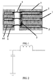
- an apparatus for improving transmission bandwidth includes: a signal transmission line 1, side grounds 2 located at two sides of the signal transmission line 1, and a capacitor 3 located between the signal transmission line 1 and the side grounds 2.
- the signal transmission line may be a microstrip line, and the signal transmission line and the side grounds form a coplanar waveguide transmission line together.
- the apparatus for improving transmission bandwidth may be applied to a transmission channel connected through a bonding wire.
- the signal transmission line 1 and the side grounds 2 are disposed on a substrate 7 having an optical component, an electric component or a photoelectric component, where the substrate 7 and a pad 61 of a package 6 are connected through a bonding wire 4.
- FIG. 2 is a schematic circuit diagram of the apparatus for improving transmission bandwidth, the bonding wire 4 presents inductance characteristics and is equivalent to an inductor.
- an LC resonance circuit is formed by using the inductance characteristics presented by the bonding wire 4 and the capacitor connected in parallel with the bonding wire 4, and a resonance point is formed within a frequency band in a frequency domain, so that a rising trend of a return loss curve is forced to slow down, thereby expanding frequency bandwidth and further expanding bandwidth of the transmission channel of a Radio Frequency (RF) signal.
- RF Radio Frequency
- the pad of the package may be a pad of an electrical interface of the photoelectric component package.
- the signal transmission line and the side grounds may be disposed on the package, for example, the signal transmission line and the side grounds may be disposed on the pad inside the package.
- the signal transmission line 1, the side grounds 2 and the capacitor 3 are disposed on the substrate 7, and moreover, the transmission line 1, the side grounds 2 and the capacitor 3 are also disposed on the package 6.
- the substrate 7 and the package 6 are connected through the bonding wire 4.
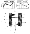
- FIG. 3 is a transmission channel connected through the bonding wire, and shows a change of a cut-off frequency point of a return loss of -10 dB before and after the capacitor is added, and a condition of insertion loss being reduced after the capacitor is adopted.
- m1 and m3 are conditions that no capacitor is disposed; m2 and m4 are conditions that an interdigital capacitor is disposed. It can be seen from FIG.
- the capacitor may be a plate capacitor, an interdigital capacitor, an MIM capacitor, or a VIC.
- the VIC when the capacitor is a VIC, the VIC includes multiple layers of metal surfaces.
- the multiple layers of metal surfaces overlap each other, and are respectively located on multiple metal conductor layers inside the substrate, where the multiple layers of metal surfaces that overlap each other form two electrodes of the VIC, and the metal surface on a top layer of the VIC is located at the same metal conductor layer with the signal transmission line.
- the multiple layers of metal surfaces located at one electrode of the VIC are connected via a through hole, and are connected to the side grounds; and the multiple layers of metal surfaces located at the other electrode of the VIC are connected to the metal surface on the top layer of the VIC via a through hole, and are connected to the signal transmission line.
- the capacitor may be integrated inside the substrate, which does not increase the area or the cost of the substrate. Moreover, the capacitor does not need to be assembled subsequently, and the capacity of the capacitor does not change with change of the external environment.
- the capacitor when the capacitor is disposed between the signal transmission line and the side grounds, if the signal transmission line or a side ground is connected to a pad, the capacitor may be connected to the signal transmission line or the side ground by being connected to the pad, thereby forming an LC resonance circuit with the bonding wire connected to the pad.
- adding the capacitor may also increase the area of the pad of the bonding wire, so that when multiple bonding wires are disposed, the distance between the bonding wires may be further increased, and the total inductance of all bonding wires connected between the substrate and the package may be reduced, thereby further improving the bandwidth of the transmission channel.
- the operation and control can be carried out more conveniently, and an error is not easily incurred, when multiple bonding wires need to be connected.
- the signal transmission line 1 and the second pad 92 (such as a signal pad) of the optical component 9 are not in the same plane, the signal transmission line 1 and the second pad 92 of the optical component 9 need to be connected through the bonding wire 4.
- the capacitor 3 may be disposed in parallel with the matching resistor 8 and disposed between the signal transmission line 1 and the side grounds 2, thereby expanding the bandwidth of the transmission channel.
- the apparatus for improving transmission bandwidth may be disposed on a TOSA, a Receiver Optical Sub-Assembly (ROSA), a Bidirectional Optical Sub-Assembly (BOSA) or a Balance Receiver (BLRX) and so on.
- the TOSA, ROSA, BOSA or BLRX may be located on the following communication devices: a 10 Gigabit Small Form Factor Pluggable Module (XFP), a Small Form Factor Pluggable Module plus (SFP+), or a 300PIN transponder.
Landscapes
- Waveguides (AREA)
- Semiconductor Integrated Circuits (AREA)
- Structure Of Printed Boards (AREA)
- Optical Modulation, Optical Deflection, Nonlinear Optics, Optical Demodulation, Optical Logic Elements (AREA)
- Semiconductor Lasers (AREA)
Applications Claiming Priority (2)
| Application Number | Priority Date | Filing Date | Title |
|---|---|---|---|
| CN200910189398.7A CN101794929B (zh) | 2009-12-26 | 2009-12-26 | 一种提升传输带宽的装置 |
| PCT/CN2010/079745 WO2011076068A1 (zh) | 2009-12-26 | 2010-12-14 | 一种提升传输带宽的装置 |
Publications (2)
| Publication Number | Publication Date |
|---|---|
| EP2432071A1 true EP2432071A1 (de) | 2012-03-21 |
| EP2432071A4 EP2432071A4 (de) | 2012-06-13 |
Family
ID=42587420
Family Applications (1)
| Application Number | Title | Priority Date | Filing Date |
|---|---|---|---|
| EP10838631A Ceased EP2432071A4 (de) | 2009-12-26 | 2010-12-14 | Vorrichtung zur erhöhung einer übertragungsbandbreite |
Country Status (4)
| Country | Link |
|---|---|
| US (1) | US8558645B2 (de) |
| EP (1) | EP2432071A4 (de) |
| CN (1) | CN101794929B (de) |
| WO (1) | WO2011076068A1 (de) |
Cited By (1)
| Publication number | Priority date | Publication date | Assignee | Title |
|---|---|---|---|---|
| WO2020219173A1 (en) * | 2019-04-24 | 2020-10-29 | Raytheon Company | Frequency selective capacitively tuned ground bonds for high isolation in rf devices |
Families Citing this family (10)
| Publication number | Priority date | Publication date | Assignee | Title |
|---|---|---|---|---|
| CN101794929B (zh) | 2009-12-26 | 2013-01-02 | 华为技术有限公司 | 一种提升传输带宽的装置 |
| CN105706223B (zh) | 2013-11-07 | 2019-02-12 | 恩智浦美国有限公司 | 键合线布置的可调损耗 |
| US9692386B2 (en) | 2013-12-23 | 2017-06-27 | Qualcomm Incorporated | Three-dimensional wire bond inductor |
| CN104836619B (zh) | 2015-03-30 | 2017-08-29 | 青岛海信宽带多媒体技术有限公司 | 一种光器件 |
| CN108063362A (zh) | 2015-03-30 | 2018-05-22 | 青岛海信宽带多媒体技术有限公司 | 一种激光器 |
| EP3845915B1 (de) * | 2018-09-20 | 2022-11-02 | Huawei Technologies Co., Ltd. | Photoelektronenkomponente und herstellungsverfahren dafür |
| CN114556724B (zh) * | 2019-10-25 | 2024-04-02 | 三菱电机株式会社 | 光半导体装置 |
| CN213342769U (zh) * | 2019-12-31 | 2021-06-01 | 华为机器有限公司 | 光发射组件、半导体光电子器件和设备 |
| CN112040643B (zh) * | 2020-09-23 | 2024-01-30 | 北京安石科技有限公司 | 一种采用并联电容的高速信号链路设计 |
| CN115831936B (zh) * | 2021-09-16 | 2023-09-05 | 安徽奥飞声学科技有限公司 | 一种具有埋容的基板及其埋容测试方法 |
Family Cites Families (15)
| Publication number | Priority date | Publication date | Assignee | Title |
|---|---|---|---|---|
| US3593208A (en) * | 1969-03-17 | 1971-07-13 | Bell Telephone Labor Inc | Microwave quadrature coupler having lumped-element capacitors |
| US4600907A (en) * | 1985-03-07 | 1986-07-15 | Tektronix, Inc. | Coplanar microstrap waveguide interconnector and method of interconnection |
| US5485131A (en) * | 1994-10-13 | 1996-01-16 | Motorola, Inc. | Transmission line filter for MIC and MMIC applications |
| US5777532A (en) * | 1997-01-15 | 1998-07-07 | Tfr Technologies, Inc. | Interdigital slow wave coplanar transmission line |
| US6057954A (en) | 1998-09-18 | 2000-05-02 | Lucent Technologies Inc. | Asymmetric inductive peaking for optoelectronic devices |
| US6242992B1 (en) * | 1999-07-30 | 2001-06-05 | Tfr Technologies, Inc. | Interdigital slow-wave coplanar transmission line resonator and coupler |
| GB0128418D0 (en) | 2001-11-28 | 2002-01-16 | Koninl Philips Electronics Nv | Dual-band antenna arrangement |
| JP2003264405A (ja) * | 2002-03-08 | 2003-09-19 | Opnext Japan Inc | 高周波伝送線路およびそれを用いた電子部品並びに電子装置 |
| US7061949B1 (en) | 2002-08-16 | 2006-06-13 | Jds Uniphase Corporation | Methods, apparatus, and systems with semiconductor laser packaging for high modulation bandwidth |
| JP3805736B2 (ja) * | 2002-10-10 | 2006-08-09 | 日本オプネクスト株式会社 | 伝送線路及びこれを用いた光モジュール |
| US7276987B2 (en) * | 2002-10-29 | 2007-10-02 | Kyocera Corporation | High frequency line-to-waveguide converter and high frequency package |
| JP4192009B2 (ja) * | 2003-02-24 | 2008-12-03 | 寛治 大塚 | 電子回路装置 |
| CN100442596C (zh) * | 2005-07-29 | 2008-12-10 | 华东师范大学 | 非周期性电容加载的移相器 |
| CN100511827C (zh) * | 2005-09-29 | 2009-07-08 | 中国科学院物理研究所 | 铁电薄膜移相器及检测与优化其反射特性的方法 |
| CN101794929B (zh) * | 2009-12-26 | 2013-01-02 | 华为技术有限公司 | 一种提升传输带宽的装置 |
-
2009
- 2009-12-26 CN CN200910189398.7A patent/CN101794929B/zh not_active Expired - Fee Related
-
2010
- 2010-12-14 EP EP10838631A patent/EP2432071A4/de not_active Ceased
- 2010-12-14 WO PCT/CN2010/079745 patent/WO2011076068A1/zh not_active Ceased
-
2011
- 2011-12-02 US US13/310,408 patent/US8558645B2/en not_active Expired - Fee Related
Cited By (1)
| Publication number | Priority date | Publication date | Assignee | Title |
|---|---|---|---|---|
| WO2020219173A1 (en) * | 2019-04-24 | 2020-10-29 | Raytheon Company | Frequency selective capacitively tuned ground bonds for high isolation in rf devices |
Also Published As
| Publication number | Publication date |
|---|---|
| WO2011076068A1 (zh) | 2011-06-30 |
| CN101794929A (zh) | 2010-08-04 |
| US8558645B2 (en) | 2013-10-15 |
| CN101794929B (zh) | 2013-01-02 |
| EP2432071A4 (de) | 2012-06-13 |
| US20120075042A1 (en) | 2012-03-29 |
Similar Documents
| Publication | Publication Date | Title |
|---|---|---|
| US8558645B2 (en) | Apparatus for improving transmission bandwidth | |
| US9413335B2 (en) | High-frequency module | |
| KR101119910B1 (ko) | 모바일 rfid 리더 송수신 시스템 | |
| US20140217570A1 (en) | Transistor outline housing and method for producing same | |
| KR101222257B1 (ko) | 다층 기판 | |
| KR101786083B1 (ko) | 데이터 통신 선로 구조 및 데이터 통신 선로 설계 방법 | |
| CN103430457B (zh) | 高频模块 | |
| US10263315B2 (en) | Directional coupler and communication module | |
| US11245386B2 (en) | High-frequency module | |
| US8060156B2 (en) | Filter having impedance matching circuits | |
| US9461619B2 (en) | High-frequency module | |
| JP2013229801A (ja) | 光受信モジュールおよび光受信機 | |
| CN100477519C (zh) | 表面声波滤波器 | |
| JP3916072B2 (ja) | 交流結合回路 | |
| US11722115B2 (en) | Radio frequency duplexer circuit and radio frequency substrate | |
| JP2009302167A (ja) | パッケージ | |
| WO2013054596A1 (ja) | 分波装置 | |
| JP5720261B2 (ja) | 電子回路及び送受信システム | |
| KR100714598B1 (ko) | 방향성 커플러 및 이를 구비한 복합소자 | |
| JP4969193B2 (ja) | 分波器 | |
| KR100442669B1 (ko) | 세라믹 커패시터의 고주파 특성 개선방법 및 이를 이용한 디씨 블록 | |
| JP2016208345A (ja) | アンテナ内蔵モジュール実装基板及びアンテナモジュールユニット | |
| KR20050053828A (ko) | 통신 모듈 측정 장치 | |
| CN110429072A (zh) | 一种倒装射频芯片及一种射频器件 | |
| JPH11251804A (ja) | 帯域阻止フィルタ |
Legal Events
| Date | Code | Title | Description |
|---|---|---|---|
| PUAI | Public reference made under article 153(3) epc to a published international application that has entered the european phase |
Free format text: ORIGINAL CODE: 0009012 |
|
| 17P | Request for examination filed |
Effective date: 20111203 |
|
| AK | Designated contracting states |
Kind code of ref document: A1 Designated state(s): AL AT BE BG CH CY CZ DE DK EE ES FI FR GB GR HR HU IE IS IT LI LT LU LV MC MK MT NL NO PL PT RO RS SE SI SK SM TR |
|
| A4 | Supplementary search report drawn up and despatched |
Effective date: 20120516 |
|
| RIC1 | Information provided on ipc code assigned before grant |
Ipc: H01P 3/08 20060101AFI20120510BHEP |
|
| DAX | Request for extension of the european patent (deleted) | ||
| 17Q | First examination report despatched |
Effective date: 20131206 |
|
| REG | Reference to a national code |
Ref country code: DE Ref legal event code: R003 |
|
| STAA | Information on the status of an ep patent application or granted ep patent |
Free format text: STATUS: THE APPLICATION HAS BEEN REFUSED |
|
| 18R | Application refused |
Effective date: 20180129 |