EP2432075B1 - Phasenverschieber, drahtlose kommunikationsvorrichtung und phasenverschiebungssteuerverfahren - Google Patents
Phasenverschieber, drahtlose kommunikationsvorrichtung und phasenverschiebungssteuerverfahren Download PDFInfo
- Publication number
- EP2432075B1 EP2432075B1 EP10774668.7A EP10774668A EP2432075B1 EP 2432075 B1 EP2432075 B1 EP 2432075B1 EP 10774668 A EP10774668 A EP 10774668A EP 2432075 B1 EP2432075 B1 EP 2432075B1
- Authority
- EP
- European Patent Office
- Prior art keywords
- signals
- phase
- phase shifter
- signal
- baseband
- Prior art date
- Legal status (The legal status is an assumption and is not a legal conclusion. Google has not performed a legal analysis and makes no representation as to the accuracy of the status listed.)
- Active
Links
Images


Classifications
-
- H—ELECTRICITY
- H04—ELECTRIC COMMUNICATION TECHNIQUE
- H04B—TRANSMISSION
- H04B7/00—Radio transmission systems, i.e. using radiation field
- H04B7/02—Diversity systems; Multi-antenna system, i.e. transmission or reception using multiple antennas
- H04B7/04—Diversity systems; Multi-antenna system, i.e. transmission or reception using multiple antennas using two or more spaced independent antennas
- H04B7/06—Diversity systems; Multi-antenna system, i.e. transmission or reception using multiple antennas using two or more spaced independent antennas at the transmitting station
- H04B7/0613—Diversity systems; Multi-antenna system, i.e. transmission or reception using multiple antennas using two or more spaced independent antennas at the transmitting station using simultaneous transmission
- H04B7/0682—Diversity systems; Multi-antenna system, i.e. transmission or reception using multiple antennas using two or more spaced independent antennas at the transmitting station using simultaneous transmission using phase diversity (e.g. phase sweeping)
-
- H—ELECTRICITY
- H04—ELECTRIC COMMUNICATION TECHNIQUE
- H04B—TRANSMISSION
- H04B7/00—Radio transmission systems, i.e. using radiation field
- H04B7/02—Diversity systems; Multi-antenna system, i.e. transmission or reception using multiple antennas
- H04B7/04—Diversity systems; Multi-antenna system, i.e. transmission or reception using multiple antennas using two or more spaced independent antennas
- H04B7/06—Diversity systems; Multi-antenna system, i.e. transmission or reception using multiple antennas using two or more spaced independent antennas at the transmitting station
- H04B7/0613—Diversity systems; Multi-antenna system, i.e. transmission or reception using multiple antennas using two or more spaced independent antennas at the transmitting station using simultaneous transmission
- H04B7/0615—Diversity systems; Multi-antenna system, i.e. transmission or reception using multiple antennas using two or more spaced independent antennas at the transmitting station using simultaneous transmission of weighted versions of same signal
-
- Y—GENERAL TAGGING OF NEW TECHNOLOGICAL DEVELOPMENTS; GENERAL TAGGING OF CROSS-SECTIONAL TECHNOLOGIES SPANNING OVER SEVERAL SECTIONS OF THE IPC; TECHNICAL SUBJECTS COVERED BY FORMER USPC CROSS-REFERENCE ART COLLECTIONS [XRACs] AND DIGESTS
- Y02—TECHNOLOGIES OR APPLICATIONS FOR MITIGATION OR ADAPTATION AGAINST CLIMATE CHANGE
- Y02D—CLIMATE CHANGE MITIGATION TECHNOLOGIES IN INFORMATION AND COMMUNICATION TECHNOLOGIES [ICT], I.E. INFORMATION AND COMMUNICATION TECHNOLOGIES AIMING AT THE REDUCTION OF THEIR OWN ENERGY USE
- Y02D30/00—Reducing energy consumption in communication networks
- Y02D30/70—Reducing energy consumption in communication networks in wireless communication networks
Definitions
- the present invention relates to a phase shifter, a wireless communication apparatus, and a phase control method.
- the present invention relates to a phase shifter, a wireless communication apparatus, and a phase control method which are capable of adding a plurality of pieces of phase information.
- each transmitter can use the band of 2.5 GHz without a license. Accordingly, the use of such a radio enables communication at a speed of 1 Gbps or higher.
- array antenna As one method to control the radiation pattern of an electromagnetic wave output from a transmitter of a wireless communication apparatus, a method using a so-called array antenna is known. Specifically, in the method, the radiation pattern is changed by controlling a phase of a signal transmitted from each antenna element.
- array antenna herein described refers to an antenna in which a plurality of antenna elements are arranged in an array.
- Non Patent Literature 1 there is a method of adding phase information to a local signal output from a local oscillator by use of a phase shifter for processing a signal in a high-frequency band, in order to control a phase of a signal transmitted from an antenna.
- the phase shifter for a high-frequency band has a great loss, and thus a new amplifier is required so as to compensate for the loss. This causes a problem of an increase in circuit size and further an increase in power consumption.
- Patent Literature 1 which is the prior application of the present application, the applicant of the present application has proposed a method of configuring a phase shifter for a baseband signal band, and adding phase information about a signal transmitted from an antenna to baseband signals, without using a phase shifter for a high-frequency band having a great loss.
- Patent Literature 1 Japanese Unexamined Patent Application Publication No. 2008-247905 US2008212706 A1 discloses a transmitter including a quadrature modulation section including a phase shifter.
- No Patent Literature 1 Arun Natarajan et al., "A 77-GHz Phased-Array Transceiver With On-Chip Antennas in Silicon: Transmitter and Local LO-Path Phase Shifting", IEEE Journal of Sclid-State Circuits, pp. 2807-2819, 2006 .
- Fig. 8 is a diagram showing configurations of a transmitting baseband phase shifter 101 and a transmitting orthogonal modulator 102 which are proposed in Patent Literature 1.
- input terminals IN1 to IN4 receive baseband signals.
- a 90° step phase shifter 103 and a signal mixer 104 (a so-called Gilbert cell mixer) add phase information to the input signals.
- the signals each including the phase information are output from output terminals OUT1 to OUT4 and transmitted to the transmitting orthogonal modulator 102.
- mixers 105-1 to 105-4 mix the signals each including the phase information with local signals distributed by a distributor 107.
- the mixed signals are combined by a combiner 106 and output from the transmitting orthogonal modulator 102.
- the Gilbert cell mixer has low power consumption
- the Gilbert cell mixer is a current drive type mixer in which more than a little current flows. Therefore, an increase in the number of antennas causes a considerable amount of power consumption in the phase shifter.
- the present invention has been made in view of the above-mentioned problems, and has an object to provide a phase shifter, a wireless communication apparatus, and a phase control method in which power consumption is reduced.
- a phase shifter is a phase shifter that adds phase information to two baseband signals to be output to an orthogonal modulator so as to control a phase of an output signal of the orthogonal modulator, the phase shifter including: a 90° step phase shifter that contributes to adding any one of phases 0°, 90°, 180°, and 270° to the baseband signals according to a first control signal; and a 45° phase shifter that contributes to adding one of phases 0° and 45° to the baseband signals according to a second control signal.
- the phase shifter performs replacement of component signals of one of the baseband signals with component signals of the other of the baseband signals and inversion of polarities of the component signals.
- a wireless communication apparatus includes a phase shifter and an array antenna.
- the phase shifter includes: a 90° step phase shifter that contributes to adding any one of phases 0°, 90°, 180°, and 270° to the baseband signals according to a first control signal; and a 45° phase shifter that contributes to adding one of phases 0° and 45° to the baseband signals according to a second control signal.
- the phase shifter performs replacement of component signals of one of the baseband signals with component signals of the other of the baseband signals and inversion of polarities of the component signals.
- phase control method that adds phase information to two baseband signals to be mixed with a local signal so as to control a phase of an output signal of an orthogonal modulator
- the phase control method comprising:performing replacement of component signals of one of the baseband signals with component signals of the other of the baseband signals and inversion of polarities of the component signals, based on phase information indicating any one of 0°, 45°, 90°, 135°, 180°, 225°, 270°, and 315°, the phase information being added to the two baseband signals to be mixed with the local signal; and executing an orthogonal modulation, wherein the execution of the orthogonal modulation includes: mixing the component signals of one of the baseband signals with local signals having relative phases of 0° and 180°, respectively, and mixing the component signals of the other of the baseband signals with local signals having relative phases of 90° and 270°, respectively, when the phase information indicates any one of 0°, 90°, 180°, and 270°; and mixing the component signals of one of
- phase shifter a phase shifter, a wireless communication apparatus, and a phase control method according to the present invention will be described with reference to the drawings.
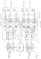
- the wireless communication apparatus shown in Fig. 1 includes a transmitter 1, a receiver 2, a transmitting baseband signal generation unit 3, a control unit 4, a receiving baseband signal processing unit 5, and a local oscillator 6.
- the transmitter 1 includes distributors 7-1 and 7-2, transmitting baseband phase shifters 8-1 to 8-n, transmitting orthogonal modulators 9-1 to 9-n, transmitting amplifiers 10-1 to 10-n, and transmitting antennas 11-1 to 11-n.
- the receiver 2 includes combiners 12-1 and 12-2, receiving baseband phase shifters 13-1 to 13-m, receiving orthogonal demodulators 14-1 to 14-m, receiving amplifiers 15-1 to 15-m, and receiving antennas 16-1 to 16-m.
- the transmitting antennas 11-1 to 11-n and the receiving antennas 16-1 to 16-m form an array antenna in which the antennas (antenna elements) are arranged in an array.
- a local signal output from the local oscillator 6 is divided into two signals to be input to the transmitter 1 and the receiver 2, respectively. In the transmitter 1, the local signal is divided into n number of signals corresponding to the antenna array number n. Similarly, also in the receiver 2, the received local signal is divided into m number of signals corresponding to the antenna array number m.
- the transmitting baseband signal generation unit 3 generates so-called I (In-phase) signal and Q (Quadrature-phase) signal from the received transmit data.
- the generated I signal and Q signal are divided into n number of signals by the distributors 7-1 and 7-2 and are input to the transmitting baseband phase shifters 8-1 to 8-n.
- the local signal output from the local oscillator 6 is divided into n number of signals to be input to the transmitting orthogonal modulators 9-1 to 9-n.
- the transmitting baseband phase shifters 8-1 to 8-n add phase information (phase control amount) corresponding to the transmitting antennas 11-1 to 11-n to the I signal and the Q signal according to a control signal output from the control unit 4.
- phase information phase control amount
- the operation and configuration of the transmitting baseband phase shifters 8-1 to 8-n will be described in detail later with reference to first to fourth exemplary embodiments to be described later.
- the I signal and the Q signal each including phase information are input to the transmitting orthogonal modulators 9-1 to 9-n.
- the transmitting orthogonal modulators 9-1 to 9-n modulate the received local signals (n number of divided local signals) according to the I signal and the Q signal each including phase information, and output the modulated signals to the transmitting amplifiers 10-1 to 10-n.
- the transmitting amplifiers 10-1 to 10-n amplify the received signals to a predetermined transmission power level, and deliver the amplified signals from the transmitting antenna11-1 to 11-n.
- the m number of divided local signals are input to the receiving orthogonal demodulators 14-1 to 14-m.
- the receiving amplifiers 15-1 to 15-m amplify signals received by the receiving antennas 16-1 to 16-m to a predetermined power level, and output the amplified signals to the receiving orthogonal demodulators 14-1 to 14-m.
- the receiving orthogonal demodulators 14-1 to 14-m demodulate the signals received from the receiving amplifiers 15-1 to 15-m with the local signals, and output the demodulated I signal and Q signal to the receiving baseband phase shifters 13-1 to 13-m.
- the receiving baseband phase shifters 13-1 to 13-m add phase information corresponding to the receiving antennas 16-1 to 16-m to the I signal and the Q signal, which are received from the receiving orthogonal demodulators 14-1 to 14-m, according to the control signal received from the control unit 4.
- the I signal and the Q signal each including phase information are combined by the combiners 12-1 and 12-2, respectively, and are input to the receiving baseband signal processing unit 5, thereby generating receive data.
- the transmitting baseband signal generation unit 3, the receiving baseband signal processing unit 5, and the control unit 4 may be implemented by hardware such as a so-called DSP (Digital Signal Processor) or may be implemented by causing a processor (CPU: Central Processing Unit) to execute the above-mentioned functions as software or programs.
- DSP Digital Signal Processor
- CPU Central Processing Unit
- These programs can be stored in various types of non-transitory computer readable media and supplied to a computer. Examples of the non-transitory computer readable media include various types of tangible storage media.
- non-transitory computer readable media include magnetic recording media (for example, flexible disks, magnetic tapes, and hard disk drives), magneto-optical media (for example, magneto-optical disks), read-only memories (CD-ROMs), CD-Rs, CD-R/Ws, and semiconductor memories (for example, mask ROMs, programmable ROMs (PROMs), erasable PROMs (EPROMs), flash ROMs, and RAMs).
- the programs may be stored in various types of transitory computer readable media to be supplied to a computer. Examples of the transitory computer readable media include electric signals, light signals, and electromagnetic waves.
- the transitory computer readable media allow the programs to be supplied to a computer through a wired communication path such as an electric wire or an optical fiber, or through a wireless communication path.
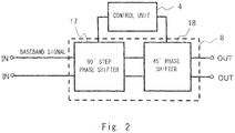
- the transmitting baseband phase shifter 8 includes a 90° step phase shifter 17 that contributes to adding phase information indicating any one of 0°, 90°, 180°, and 270°, and a 45° phase shifter 18 that contributes to adding phases of 0° and 45°.
- the 90° step phase shifter 17 and the 45°phase shifter 18 add phase information corresponding to the control signal to baseband signals based on the control signal from the control unit 4. Specifically, the 90° step phase shifter 17 and the 45° phase shifter 18 perform replacement of component signals of one of the baseband signals with component signals of the other of the baseband signals and inversion of polarities of the component signals. According to the configuration example shown in Fig. 2 , a Gilbert cell mixer is not used, thereby making it possible to reduce the power consumption in the phase shifter to approximately zero.
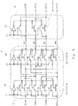
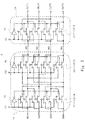
- the 90° step phase shifter 17 includes at least two inverters 19 and 20 and at least 16 switches (switching elements) 21-1 to 21-8 and 22-1 to 22-8.
- the switches 21-1 to 21-8 are controlled by a control signal C1
- the switches 22-1 to 22-8 are controlled by a control signal C2.
- the control signals C1 and C2 are supplied from the control unit 4.
- the I signal which is a differential signal, is input to each of an input terminal IN1 and an input terminal IN2 of the transmitting baseband phase shifter 8.
- the Q signal is input to each of an input terminal IN3 and an input terminal IN4. Paths for the input I signal and Q signal are switched by the control signal C1 and the control signal C2.
- the I signal and the Q signal are output from output terminals M1, M2, M3, and M4 depending on the switching state.
- the baseband signals output to the output terminal M1 and the output terminal M2 are a differential pair.
- the baseband signals output to the output terminal M3 and the output terminal M4 are also a differential pair.
- the 45° phase shifter 18 includes at least one inverter 23 and at least four switching elements 24-1 to 24-4.
- the switches 24-1 to 24-4 are controlled by a control signal C3.
- the control signal C3 is supplied from the control unit 4, as with the control signals C1 and C2.
- the 45° phase shifter 18 directly outputs the I signal and the Q signal, which are output from the 90° step phase shifter 17, to the transmitting orthogonal modulator, without performing any other operation on the I signal and the Q signal.
- the 45° phase shifter 18 branches a signal having one polarity among component signals of one of the baseband signals of the received I signal and Q signal into two signals, and outputs the two signals from the output terminal OUT1 and the output terminal OUT3.
- the 45° phase shifter 18 blocks a signal having the other polarity among the component signals of the baseband signal.
- the 45° phase shifter 18 outputs component signals of the baseband signal, which are not branched and blocked, from the output terminal OUT2 and the output terminal OUT4.
- Table 1 is a table showing the relation between the phase information and output signals in the first exemplary embodiment of the present invention.
- the 90° step phase shifter 17 and the 45° phase shifter 18 perform replacement of signals +I, -I, +Q, and -Q and inversion of polarities as illustrated in Table 1.
- the baseband signal output from the output terminal OUT1 of the transmitting baseband phase shifter 8 is input to the mixer 105-1, which receives a local signal having a relative phase of 0°, of the transmitting orthogonal modulator 102 in the same manner as in the transmitting baseband phase shifter 101 shown in Fig. 8 .
- the baseband signal output from the output terminal OUT2 is input to the mixer 105-2 which receives a local signal having a relative phase of 180°.
- the baseband signal output from the output terminal OUT3 is input to the mixer 105-3 which receives a local signal having a relative phase of 90°.
- the baseband signal output from the output terminal OUT4 is input to the mixer 105-4 which receives a local signal having a relative phase of 270°.
- values 0 and 1 are used to indicate each state of the control signals C1, C2, and C3.
- the values respectively represent a low voltage level ("0" logical level) and a high voltage level ("1" logical level) of the control signals (C1, C2, and C3). If the relation of the input-output is the same, the states of each control signal are not limited to those shown in table 1. Further, when it is a circuit satisfying the relation of table 1, the number of inverters and switches are not limited to the numbers shown in FIG. 3 .
- control unit 4 can refer to the information shown in Table 1 from the inside or from the outside of the control unit 4 as a table (look-up table), for example. In this case, the control unit 4 determines a combination of the control signals C1, C2, and C3 to be output according to the required phase.
- the phrase "can refer to the information from the inside of the control unit” means referring to a look-up table stored in a register provided in the control unit 4, for example.
- the look-up table is a loaded look-up table stored in an external storage medium (for example, a hard disk drive (HDD) or a flash memory) simultaneously with power ON.
- HDD hard disk drive
- the transmitting baseband phase shifter 8 serving as the transmitting baseband phase shifters 8-1 to 8-n adds phase information indicating any one of 0°, 45°, 90°, 135°, 180°, 225°, 270°, and 315°. This enables reduction in power consumption to approximately zero and setting of the resolution of added phase information to 45°.
- the transmitting baseband phase shifter 8 shown in Fig. 4 includes the transmitting baseband phase shifters 8-1 to 8-n shown in Fig. 1 .
- the transmitting baseband phase shifter 8 shown in Fig. 4 adds phase information indicating any one of 0°, 45°, 90°, 135°, 180°, 225°, 270°, and 315° to baseband signals output from the transmitting baseband signal generation unit 3.
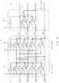
- the baseband phase shifter 8 includes the 90° step phase shifter 17 that contributes to a 90° step phase change, and a 45° phase shifter 25 that contributes to a 45° phase change.
- the 90° step phase shifter 17 is identical with that of the first exemplary embodiment, so the description thereof is omitted.
- the 45° phase shifter 25 includes an inverter 26 that inverts a control signal, an inverter 27 that inverts polarities of baseband signals, and at least four switching elements 28-1 to 28-4.
- the switches 28-1 to 28-4 are controlled by the control signal C3.
- the control signal C3 is supplied from the control unit 4, as with the control signals C1 and C2.
- the path switching is executed based on the relation between the phase information ( ⁇ ) and output signals shown in Table 1 according to the phase information to be added.
- the 45° phase shifter 25 outputs a signal having one polarity among component signals of one of the baseband signals of the received I signal and Q signal from the output terminal OUT1.
- the inverter 27 inverts the polarity of a signal having the other polarity among the component signals of the baseband signal, and the inverted signal is output from the output terminal OUT3.
- the 45° phase shifter 25 outputs component signals of the baseband signal, which are not branched and blocked, from the output terminal OUT2 and the output terminal OUT4. Consequently, the relation between the phase information and output signals shown in Table 1 can be achieved without branching the component signals of the baseband signals.
- the baseband signals output from the output terminals OUT1 to OUT4 of the transmitting baseband phase shifter 8 are input to the orthogonal modulator as in the first exemplary embodiment.
- the transmitting baseband phase shifter 8 shown in Fig. 5 constitutes the transmitting baseband phase shifters 8-1 to 8-n shown in Fig. 1 .
- the transmitting baseband phase shifter 8 shown in Fig. 5 adds phase information indicating any one of 0°, 45°, 90°, 135°, 180°, 225°, 270°, and 315° to baseband signals output from the transmitting baseband signal generation unit 3.
- the baseband phase shifter 8 includes the 90° step phase shifter 17 that contributes to a 90° step phase change, and a 45° phase shifter 29 that contributes to a 45° phase change.
- the 90° step phase shifter 17 is identical with that of the first exemplary embodiment, so the description thereof is omitted.
- the 45° phase shifter 29 includes at least one inverter 30 and eight switching elements 31-1 to 31-8.
- the switches 31-1 to 31-8 are controlled by the control signal C3.
- the control signal C3 is supplied from the control unit 4, as with the control signals C1 and C2.
- the path switching is executed based on the relation between the phase information ( ⁇ ) and output signals shown in Table 1 according to the phase information to be added.
- the switches 31-1, 31-4, 31-5, and 31-6 are disposed at the same positions as the switches 24-1 to 24-4 shown in Fig. 3 and contribute to a 45° phase change.
- the provision of the other switches 31-2, 31-3, 31-7, and 31-8 enables compensation for a delay associated with the path switching in the 45° phase shifter 29. Assume that among the switches 31, the switch 31-1 is located at the top of Fig. 5 and the switch 31-8 is located at the bottom of Fig. 5 .
- the base band signals output from the output terminals OUT1 to OUT4 of the transmitting baseband phase shifter 8 are input to the orthogonal modulator as in the first exemplary embodiment.
- the transmitting baseband phase shifter 8 shown in Fig. 6 includes the transmitting baseband phase shifters 8-1 to 8-n shown in Fig. 1 .
- the transmitting baseband phase shifter 8 shown in Fig. 5 adds phase information indicating any one of 0°, 45°, 90°, 135°, 180°, 225°, 270°, and 315° to baseband signals output from the transmitting baseband signal generation unit 3.
- the baseband phase shifter 8 includes the 90° step phase shifter 17 that contributes to a 90° step phase change, and the 45° phase shifter 29 that contributes to a 45° phase change.
- the 45° phase shifter 29 has output terminals respectively connected to gain variable amplifiers 32-1 to 32-4.
- the 90° step phase shifter 17 and the 45° phase shifter 29 are identical with those of the third exemplary embodiment, so the description thereof is omitted.
- the gain variable amplifiers 32-1 to 32-4 change the amplitude of each baseband signal output from the 45° phase shifter 29 according to a control signal C4 from the control unit 4.
- the gain of each of the gain variable amplifiers 32-1 to 32-4 is variable. This makes it possible to correct an amplitude error generated in the 90° step phase shifter 17 and the 45° phase shifter 29.
- the baseband signals output from the output terminals OUT1, OUT2, OUT3, and OUT4 of the transmitting baseband phase shifter 8 are input to the orthogonal modulator as in the first exemplary embodiment.
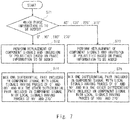
- the control unit 4 determines which one of the phase information indicating any one of 0°, 90°, 180°, and 270° and the phase information indicating any one of 45°, 135°, 225°, and 315° is added to the baseband signals (S71).
- the transmitting baseband phase shifter 8 performs replacement of the component signals +I, -I, +Q, and -Q of the baseband signals and inversion of polarities according to the relation between the phase information ( ⁇ ) and output signals illustrated in Table 1 (S72, S73).
- the transmitting orthogonal modulators 9 mix a differential pair of signals forming one of the I signal and the Q signal with local signals having relative phases of 0° and 180°, respectively. Further, the transmitting orthogonal modulators 9 mix a differential pair of signals forming the other of the baseband signals with local signals having relative phases of 90° and 270°, respectively (S74).
- the transmitting orthogonal modulators 9 mix a differential pair of signals forming one of the I signal and the Q signal with local signals having relative phases of 0° and 90°, respectively. Further, the transmitting orthogonal modulators 9 mix a differential pair of signals forming the other of the baseband signals with local signals having relative phases of 180° and 270°, respectively (S75). This enables phase control with a phase resolution of 45°.
Landscapes
- Engineering & Computer Science (AREA)
- Computer Networks & Wireless Communication (AREA)
- Signal Processing (AREA)
- Transmitters (AREA)
- Waveguide Switches, Polarizers, And Phase Shifters (AREA)
- Variable-Direction Aerials And Aerial Arrays (AREA)
- Circuits Of Receivers In General (AREA)
- Radio Transmission System (AREA)
Claims (13)
- Phasenschieber (8) zum Empfangen von Komponentensignalen von zwei Basisbandsignalen und zum Hinzufügen von Phaseninformation zu den zwei Basisbandsignalen, der Folgendes umfasst:einen 90°-Stufenphasenschieber (17), der angepasst ist, zum Hinzufügen von einer der Phasen 0°, 90°, 180° und 270° zu den Basisbandsignalen entsprechend einem ersten Steuersignal (C1, C2) beizutragen; undeinen 45°-Phasenschieber (18), der angepasst ist, zum Hinzufügen einer der Phasen 0° und 45° zu den Basisbandsignalen, die von dem 90°-Stufenphasenschieber ausgegeben werden, entsprechend einem zweiten Steuersignal (C3) beizutragen;wobei der Phasenschieber angepasst ist, den Ersatz von Komponentensignalen von einem der Basisbandsignale durch Komponentensignale des anderen der Basisbandsignale und Inversion von Polaritäten der Komponentensignale durchzuführen, und wobei der Phasenschieber weiter angepasst ist, die zwei Basisbandsignale einschließlich der Phaseninformation an einen orthogonalen Modulator auszugeben, um so eine Phase eines Ausgangssignals des orthogonalen Modulators zu steuern.
- Phasenschieber (8) gemäß Anspruch 1, wobei
die Phaseninformation einen der Werte 0°, 45°, 90°, 135°, 180°, 225°, 270° und 315° angibt und
wobei der Phasenschieber so angepasst ist, dass, wenn die Phaseninformation eines von 0°, 90°, 180° und 270° angibt, der Phasenschieber die Komponentensignale von einem der Basisbandsignale, die von dem Phasenschieber empfangen werden, an die Mischer ausgibt, die lokale Signale empfangen, die jeweils relative Phasen von 0° und 180° aufweisen, unter den Mischern, die den orthogonalen Modulator bilden, und die Komponentensignale der anderen der Basisbandsignale an die Mischer ausgibt, die lokale Signale empfangen, die jeweils relative Phasen von 90° und 270° aufweisen, unter den Mischern, und
wobei der Phasenschieber daran angepasst ist, dass, wenn die Phaseninformation eines von 45°, 135°, 225° und 315° angibt, der Phasenschieber die Komponentensignale eines der Basisbandsignale an die Mischer ausgibt, welche die lokalen Signale empfangen, die jeweils die relativen Phasen von 0° und 90° aufweisen, und die Komponentensignale der anderen der Basisbandsignale an die Mischer ausgibt, welche die lokalen Signale empfangen, die jeweils die relativen Phasen von 180° und 270° aufweisen, unter den Mischern, die den orthogonalen Modulator bilden. - Phasenschieber (8) gemäß Anspruch 1 oder 2, wobei
der Phasenschieber so angepasst ist, dass, wenn die Phaseninformation eines von 45°, 135°, 225° und 315° angibt, der Phasenschieber die Komponentensignale von einem der Basisbandsignale an die Mischer ausgibt, die lokale Signale empfangen, die jeweils relative Phasen von 0° und 90° aufweisen, unter den Mischern, die den orthogonalen Modulator bilden, und
der Phasenschieber ein Signal, das eine Polarität unter den Komponentensignalen der Basisbandsignale aufweist, in zwei Signale verzweigt, die zwei verzweigten Signale an die Mischer ausgibt, welche die lokalen Signale empfangen, die jeweils die relativen Phasen von 0° und 90° aufweisen, und ein Signal, dass die andere Polarität aufweist, blockiert. - Phasenschieber (8) gemäß Anspruch 1 oder 2, wobei
der Phasenschieber so angepasst ist, dass, wenn die Phaseninformation eines von 45°, 135°, 225° und 315° angibt, der Phasenschieber die Komponentensignale von einem der Basisbandsignale an die Mischer ausgibt, die lokale Signale empfangen, die jeweils relative Phasen von 0° und 90° aufweisen, unter den Mischern, die den orthogonalen Modulator bilden, und
der Phasenschieber ein Signal, das eine Polarität aufweist, unter den Komponentensignalen der Basisbandsignale an den Mischer ausgibt, der das lokale Signal empfängt, das die relative Phase von 0° aufweist, unter den Mischern, die den orthogonalen Modulator bilden, und eine Polarität eines Signals, das die andere Polarität aufweist, invertiert und das invertierte Signal an den Mischer ausgibt, der das lokale Signal empfängt, das die relative Phase von 90° aufweist. - Phasenschieber (8) gemäß einem der Ansprüche 1 bis 4, wobei der 45°-Phasenschieber ein Verzögerungselement für jeden Pfad einschließt.
- Phasenschieber (8) gemäß Anspruch 5, wobei das Verzögerungselement ein Schaltelement zum Schalten jedes Pfades ist.
- Phasenschieber (8) gemäß einem der Ansprüche 1 bis 6, der weiter einen Signalverstärker mit variabler Verstärkung umfasst, wobei der Signalverstärker an einem Ausgang des 45°-Phasenschieber angeordnet ist.
- Drahtlose Kommunikationsvorrichtung, die Folgendes umfasst:einen Phasenschieber (8) gemäß einem der Ansprüche 1 bis 7; undeine Antennengruppe.
- Drahtloser Sender, der Folgendes umfasst:einen Phasenschieber (8) gemäß einem der Ansprüche 1 bis 7; undeine Antennengruppe.
- Drahtloser Empfänger, der Folgendes umfasst:einen Phasenschieber (8) gemäß einem der Ansprüche 1 bis 7; undeine Antennengruppe.
- Phasensteuerverfahren zum Hinzufügen von Phaseninformation zu zwei Basisbandsignalen zur Mischung mit einem lokalen Signal, um so eine Phase eines Ausgangssignals eines orthogonalen Modulators zu steuern, wobei das Phasensteuerverfahren Folgendes umfasst:Erzeugen der lokalen Signale durch einen lokalen Oszillator,Durchführen von Ersetzung (S72, S73) von Komponentensignalen von einem der Basisbandsignale durch Komponentensignale des anderen der Basisbandsignale und Inversion von Polaritäten der Komponentensignale, basierend auf Phaseninformation, die eines von 0°, 45°, 90°, 135°, 180°, 225°, 270° und 315° angibt, wobei die Phaseninformation zu den zwei Basisbandsignalen zur Mischung mit dem lokalen Signal hinzugefügt wird; undAusführen einer orthogonalen Modulation basierend auf den Basisbandsignalen einschließlich der Phaseninformation,wobei die Ausführung der orthogonalen Modulation einschließt:Mischen (S74) der Komponentensignale eines der Basisbandsignale mit lokalen Signalen, die jeweils relative Phasen von 0 und 180° aufweisen, und mischen der Komponentensignale des anderen der Basisbandsignale mit lokalen Signalen, die jeweils relative Phasen von 90° und 270° aufweisen, wenn die Phaseninformation eines von 0°, 90°, 180° und 270° angibt; undMischen (S75) der Komponentensignale eines der Basisbandsignale mit den lokalen Signalen, die jeweils die relativen Phasen von 0° und 90° aufweisen, und Mischen der Komponentensignale des anderen der Basisbandsignale mit den lokalen Signalen, die jeweils die relativen Phasen von 180° und 270° aufweisen, wenn die Phaseninformation eines von 45°, 135°, 225° und 315° angibt.
- Phasensteuerverfahren gemäß Anspruch 11, wobei,
wenn die Phaseninformation eines von 45°, 135°, 225° und 315° angibt, ein Signal, das eine Polarität unter den Komponentensignalen von einem der Basisbandsignale aufweist, in zwei Signale aufgeteilt wird und
die zwei Signale mit den lokalen Signalen, die jeweils die relativen Phasen von 0° und 90° aufweisen, gemischt werden und ein Signal, das die andere Polarität aufweist, blockiert wird. - Phasensteuerverfahren gemäß Anspruch 11, wobei
wenn die Phaseninformation eines von 45°, 135°, 225° und 315° angibt, ein Signal, das eine Polarität unter den Komponentensignalen von einem der Basisbandsignale aufweist, mit dem lokalen Signal gemischt wird, das die relative Phase von 0° aufweist, und die Polarität eines Signals, das die andere Polarität aufweist, invertiert wird und mit dem lokalen Signal, das die relative Phase von 90° aufweist, gemischt wird.
Applications Claiming Priority (2)
| Application Number | Priority Date | Filing Date | Title |
|---|---|---|---|
| JP2009117221 | 2009-05-14 | ||
| PCT/JP2010/002221 WO2010131408A1 (ja) | 2009-05-14 | 2010-03-26 | 移相器、無線通信装置及び位相制御方法 |
Publications (3)
| Publication Number | Publication Date |
|---|---|
| EP2432075A1 EP2432075A1 (de) | 2012-03-21 |
| EP2432075A4 EP2432075A4 (de) | 2017-04-26 |
| EP2432075B1 true EP2432075B1 (de) | 2018-11-14 |
Family
ID=43084794
Family Applications (1)
| Application Number | Title | Priority Date | Filing Date |
|---|---|---|---|
| EP10774668.7A Active EP2432075B1 (de) | 2009-05-14 | 2010-03-26 | Phasenverschieber, drahtlose kommunikationsvorrichtung und phasenverschiebungssteuerverfahren |
Country Status (4)
| Country | Link |
|---|---|
| US (1) | US8665989B2 (de) |
| EP (1) | EP2432075B1 (de) |
| JP (1) | JP5360204B2 (de) |
| WO (1) | WO2010131408A1 (de) |
Families Citing this family (3)
| Publication number | Priority date | Publication date | Assignee | Title |
|---|---|---|---|---|
| US9584231B2 (en) * | 2014-10-30 | 2017-02-28 | Samsung Electronics Co., Ltd. | Integrated two dimensional active antenna array communication system |
| KR101624287B1 (ko) | 2015-01-14 | 2016-05-25 | (주)엑스엠더블유 | 효율적인 디지털 위상변화기 |
| CN116886114A (zh) * | 2023-06-21 | 2023-10-13 | 北京巨束科技有限公司 | 信号相位补偿方法、相控阵及其控制方法、设备及介质 |
Family Cites Families (19)
| Publication number | Priority date | Publication date | Assignee | Title |
|---|---|---|---|---|
| US5535244A (en) * | 1993-06-07 | 1996-07-09 | Matsushita Electric Industrial Co., Ltd. | Digital modulating/demodulating apparatus and a digital demodulating apparatus |
| US5748680A (en) * | 1994-12-16 | 1998-05-05 | Lucent Technologies Inc. | Coarse frequency burst detector for a wireline communications system |
| JP3252639B2 (ja) * | 1995-03-03 | 2002-02-04 | 三菱電機株式会社 | 検波器及び受信装置並びに送信装置 |
| JP3608765B2 (ja) * | 1998-02-25 | 2005-01-12 | アイコム株式会社 | 周波数シンセサイザ装置 |
| JP3252820B2 (ja) * | 1999-02-24 | 2002-02-04 | 日本電気株式会社 | 復調及び変調回路並びに復調及び変調方法 |
| US6320480B1 (en) * | 1999-10-26 | 2001-11-20 | Trw Inc. | Wideband low-loss variable delay line and phase shifter |
| CN1379928A (zh) * | 2000-08-21 | 2002-11-13 | 三菱电机株式会社 | π/2移相器 |
| US6748024B2 (en) * | 2001-03-28 | 2004-06-08 | Nokia Corporation | Non-zero complex weighted space-time code for multiple antenna transmission |
| US6983024B2 (en) * | 2003-03-18 | 2006-01-03 | Qualcomm Inc. | Quadra-polar modulator |
| JP4443973B2 (ja) * | 2004-03-29 | 2010-03-31 | 三菱電機株式会社 | 移相器 |
| JP2006086857A (ja) * | 2004-09-16 | 2006-03-30 | Matsushita Electric Ind Co Ltd | 移相装置 |
| US8170130B2 (en) * | 2005-03-28 | 2012-05-01 | Panasonic Corporation | Transmission method and transmission system |
| WO2006126462A1 (ja) * | 2005-05-24 | 2006-11-30 | Matsushita Electric Industrial Co., Ltd. | 放送システム、ラジオ受信機、電子機器及びラジオ放送用変復調方法 |
| US7545856B2 (en) * | 2005-09-08 | 2009-06-09 | Broadcom Corporation | Current mode phase shifter, mixer and amplifier |
| US20070160168A1 (en) * | 2006-01-11 | 2007-07-12 | Beukema Troy J | Apparatus and method for signal phase control in an integrated radio circuit |
| JP4172805B2 (ja) * | 2006-07-12 | 2008-10-29 | 株式会社東芝 | 通信装置、直交誤差補償の設定値算出方法および直交誤差補償プログラム |
| US7904045B2 (en) * | 2006-08-04 | 2011-03-08 | Axiom Microdevices, Inc. | Phase detector comprising a switch configured to select a phase offset closest to a phase of an amplifier |
| EP1977743B1 (de) | 2007-03-20 | 2009-09-02 | Johnson & Johnson Consumer France SAS | Zusammensetzung enthältend Retinoid und Beta-aminoisobuttersäurederivate |
| JP2009117221A (ja) | 2007-11-08 | 2009-05-28 | Toyota Motor Corp | スタック構造を有する燃料電池 |
-
2010
- 2010-03-26 EP EP10774668.7A patent/EP2432075B1/de active Active
- 2010-03-26 JP JP2011513220A patent/JP5360204B2/ja active Active
- 2010-03-26 US US13/264,046 patent/US8665989B2/en active Active
- 2010-03-26 WO PCT/JP2010/002221 patent/WO2010131408A1/ja not_active Ceased
Non-Patent Citations (1)
| Title |
|---|
| None * |
Also Published As
| Publication number | Publication date |
|---|---|
| EP2432075A4 (de) | 2017-04-26 |
| JP5360204B2 (ja) | 2013-12-04 |
| EP2432075A1 (de) | 2012-03-21 |
| US8665989B2 (en) | 2014-03-04 |
| US20120039370A1 (en) | 2012-02-16 |
| JPWO2010131408A1 (ja) | 2012-11-01 |
| WO2010131408A1 (ja) | 2010-11-18 |
Similar Documents
| Publication | Publication Date | Title |
|---|---|---|
| US10171141B2 (en) | Hybrid beam-forming antenna array using selection matrix for antenna phase calibration | |
| US7697958B2 (en) | Wireless repeater | |
| CN108390703B (zh) | 一种多波束相控阵天线机构 | |
| CN106602265B (zh) | 波束成形网络及其输入结构、输入输出方法及三波束天线 | |
| US9287960B2 (en) | Radio communication apparatus, transmitter, and radio communication method | |
| CN114902493B (zh) | 相控阵模块 | |
| EP3739763B1 (de) | Kommunikationsvorrichtung | |
| EP2820774B1 (de) | Hf-strahlformung in einer phasengesteuerten gruppenanwendung | |
| CN112737511B (zh) | 具有相移功能的混频器及包括所述混频器的通信设备 | |
| US20060003808A1 (en) | Mobile radio base station | |
| US10700755B2 (en) | Antenna mapping and diversity | |
| US20180109404A1 (en) | Wireless Transceiver for Transmitting Circularly-Polarized Signals with Modulated Angular Speed | |
| US10256553B2 (en) | Efficient multi-polarization communications | |
| US11641228B2 (en) | Flexible beamforming architecture | |
| CN115004479B (zh) | 用于控制天线阵列的方法和系统 | |
| CN106603129B (zh) | 一种多天线的mimo系统 | |
| CN203277650U (zh) | 一种多波束宽度天线系统和馈电网络 | |
| KR101847133B1 (ko) | 단일의 이중편파 복사소자에 의한 4중편파 안테나 장치 | |
| WO2009101993A1 (ja) | 移相器及びその制御方法、アレイアンテナを備える無線通信装置 | |
| EP2432075A1 (de) | Phasenverschieber, drahtlose kommunikationsvorrichtung und phasenverschiebungssteuerverfahren | |
| US6738019B1 (en) | Apparatus and method for driving a sectored antenna | |
| EP3847747B1 (de) | Lokaloszillatorverteilungsnetzwerk mit kaskadiertem senden und empfangen | |
| US20230179237A1 (en) | Transmitter arrangement, transceiver, radio communication system and method | |
| CN206003971U (zh) | 波束成形网络及其输入结构、三波束天线 | |
| US11923878B2 (en) | Wireless signal processing circuit and wireless device |
Legal Events
| Date | Code | Title | Description |
|---|---|---|---|
| PUAI | Public reference made under article 153(3) epc to a published international application that has entered the european phase |
Free format text: ORIGINAL CODE: 0009012 |
|
| 17P | Request for examination filed |
Effective date: 20111013 |
|
| AK | Designated contracting states |
Kind code of ref document: A1 Designated state(s): AT BE BG CH CY CZ DE DK EE ES FI FR GB GR HR HU IE IS IT LI LT LU LV MC MK MT NL NO PL PT RO SE SI SK SM TR |
|
| DAX | Request for extension of the european patent (deleted) | ||
| RA4 | Supplementary search report drawn up and despatched (corrected) |
Effective date: 20170328 |
|
| RIC1 | Information provided on ipc code assigned before grant |
Ipc: H04J 11/00 20060101ALI20170322BHEP Ipc: H04B 7/08 20060101ALI20170322BHEP Ipc: H04B 7/10 20170101ALI20170322BHEP Ipc: H01Q 23/00 20060101AFI20170322BHEP Ipc: H04J 99/00 20090101ALI20170322BHEP |
|
| GRAP | Despatch of communication of intention to grant a patent |
Free format text: ORIGINAL CODE: EPIDOSNIGR1 |
|
| STAA | Information on the status of an ep patent application or granted ep patent |
Free format text: STATUS: GRANT OF PATENT IS INTENDED |
|
| INTG | Intention to grant announced |
Effective date: 20180615 |
|
| GRAS | Grant fee paid |
Free format text: ORIGINAL CODE: EPIDOSNIGR3 |
|
| GRAA | (expected) grant |
Free format text: ORIGINAL CODE: 0009210 |
|
| STAA | Information on the status of an ep patent application or granted ep patent |
Free format text: STATUS: THE PATENT HAS BEEN GRANTED |
|
| AK | Designated contracting states |
Kind code of ref document: B1 Designated state(s): AT BE BG CH CY CZ DE DK EE ES FI FR GB GR HR HU IE IS IT LI LT LU LV MC MK MT NL NO PL PT RO SE SI SK SM TR |
|
| REG | Reference to a national code |
Ref country code: GB Ref legal event code: FG4D |
|
| REG | Reference to a national code |
Ref country code: CH Ref legal event code: EP Ref country code: AT Ref legal event code: REF Ref document number: 1065935 Country of ref document: AT Kind code of ref document: T Effective date: 20181115 |
|
| REG | Reference to a national code |
Ref country code: DE Ref legal event code: R096 Ref document number: 602010055122 Country of ref document: DE |
|
| REG | Reference to a national code |
Ref country code: DE Ref legal event code: R082 Ref document number: 602010055122 Country of ref document: DE Representative=s name: GLAWE DELFS MOLL PARTNERSCHAFT MBB VON PATENT-, DE |
|
| REG | Reference to a national code |
Ref country code: IE Ref legal event code: FG4D |
|
| REG | Reference to a national code |
Ref country code: NL Ref legal event code: MP Effective date: 20181114 |
|
| REG | Reference to a national code |
Ref country code: LT Ref legal event code: MG4D |
|
| REG | Reference to a national code |
Ref country code: AT Ref legal event code: MK05 Ref document number: 1065935 Country of ref document: AT Kind code of ref document: T Effective date: 20181114 |
|
| PG25 | Lapsed in a contracting state [announced via postgrant information from national office to epo] |
Ref country code: AT Free format text: LAPSE BECAUSE OF FAILURE TO SUBMIT A TRANSLATION OF THE DESCRIPTION OR TO PAY THE FEE WITHIN THE PRESCRIBED TIME-LIMIT Effective date: 20181114 Ref country code: HR Free format text: LAPSE BECAUSE OF FAILURE TO SUBMIT A TRANSLATION OF THE DESCRIPTION OR TO PAY THE FEE WITHIN THE PRESCRIBED TIME-LIMIT Effective date: 20181114 Ref country code: BG Free format text: LAPSE BECAUSE OF FAILURE TO SUBMIT A TRANSLATION OF THE DESCRIPTION OR TO PAY THE FEE WITHIN THE PRESCRIBED TIME-LIMIT Effective date: 20190214 Ref country code: ES Free format text: LAPSE BECAUSE OF FAILURE TO SUBMIT A TRANSLATION OF THE DESCRIPTION OR TO PAY THE FEE WITHIN THE PRESCRIBED TIME-LIMIT Effective date: 20181114 Ref country code: LT Free format text: LAPSE BECAUSE OF FAILURE TO SUBMIT A TRANSLATION OF THE DESCRIPTION OR TO PAY THE FEE WITHIN THE PRESCRIBED TIME-LIMIT Effective date: 20181114 Ref country code: IS Free format text: LAPSE BECAUSE OF FAILURE TO SUBMIT A TRANSLATION OF THE DESCRIPTION OR TO PAY THE FEE WITHIN THE PRESCRIBED TIME-LIMIT Effective date: 20190314 Ref country code: NO Free format text: LAPSE BECAUSE OF FAILURE TO SUBMIT A TRANSLATION OF THE DESCRIPTION OR TO PAY THE FEE WITHIN THE PRESCRIBED TIME-LIMIT Effective date: 20190214 Ref country code: FI Free format text: LAPSE BECAUSE OF FAILURE TO SUBMIT A TRANSLATION OF THE DESCRIPTION OR TO PAY THE FEE WITHIN THE PRESCRIBED TIME-LIMIT Effective date: 20181114 Ref country code: LV Free format text: LAPSE BECAUSE OF FAILURE TO SUBMIT A TRANSLATION OF THE DESCRIPTION OR TO PAY THE FEE WITHIN THE PRESCRIBED TIME-LIMIT Effective date: 20181114 |
|
| PG25 | Lapsed in a contracting state [announced via postgrant information from national office to epo] |
Ref country code: GR Free format text: LAPSE BECAUSE OF FAILURE TO SUBMIT A TRANSLATION OF THE DESCRIPTION OR TO PAY THE FEE WITHIN THE PRESCRIBED TIME-LIMIT Effective date: 20190215 Ref country code: SE Free format text: LAPSE BECAUSE OF FAILURE TO SUBMIT A TRANSLATION OF THE DESCRIPTION OR TO PAY THE FEE WITHIN THE PRESCRIBED TIME-LIMIT Effective date: 20181114 Ref country code: NL Free format text: LAPSE BECAUSE OF FAILURE TO SUBMIT A TRANSLATION OF THE DESCRIPTION OR TO PAY THE FEE WITHIN THE PRESCRIBED TIME-LIMIT Effective date: 20181114 Ref country code: PT Free format text: LAPSE BECAUSE OF FAILURE TO SUBMIT A TRANSLATION OF THE DESCRIPTION OR TO PAY THE FEE WITHIN THE PRESCRIBED TIME-LIMIT Effective date: 20190314 |
|
| PG25 | Lapsed in a contracting state [announced via postgrant information from national office to epo] |
Ref country code: DK Free format text: LAPSE BECAUSE OF FAILURE TO SUBMIT A TRANSLATION OF THE DESCRIPTION OR TO PAY THE FEE WITHIN THE PRESCRIBED TIME-LIMIT Effective date: 20181114 Ref country code: PL Free format text: LAPSE BECAUSE OF FAILURE TO SUBMIT A TRANSLATION OF THE DESCRIPTION OR TO PAY THE FEE WITHIN THE PRESCRIBED TIME-LIMIT Effective date: 20181114 Ref country code: CZ Free format text: LAPSE BECAUSE OF FAILURE TO SUBMIT A TRANSLATION OF THE DESCRIPTION OR TO PAY THE FEE WITHIN THE PRESCRIBED TIME-LIMIT Effective date: 20181114 Ref country code: IT Free format text: LAPSE BECAUSE OF FAILURE TO SUBMIT A TRANSLATION OF THE DESCRIPTION OR TO PAY THE FEE WITHIN THE PRESCRIBED TIME-LIMIT Effective date: 20181114 |
|
| REG | Reference to a national code |
Ref country code: DE Ref legal event code: R097 Ref document number: 602010055122 Country of ref document: DE |
|
| PG25 | Lapsed in a contracting state [announced via postgrant information from national office to epo] |
Ref country code: RO Free format text: LAPSE BECAUSE OF FAILURE TO SUBMIT A TRANSLATION OF THE DESCRIPTION OR TO PAY THE FEE WITHIN THE PRESCRIBED TIME-LIMIT Effective date: 20181114 Ref country code: EE Free format text: LAPSE BECAUSE OF FAILURE TO SUBMIT A TRANSLATION OF THE DESCRIPTION OR TO PAY THE FEE WITHIN THE PRESCRIBED TIME-LIMIT Effective date: 20181114 Ref country code: SM Free format text: LAPSE BECAUSE OF FAILURE TO SUBMIT A TRANSLATION OF THE DESCRIPTION OR TO PAY THE FEE WITHIN THE PRESCRIBED TIME-LIMIT Effective date: 20181114 Ref country code: SK Free format text: LAPSE BECAUSE OF FAILURE TO SUBMIT A TRANSLATION OF THE DESCRIPTION OR TO PAY THE FEE WITHIN THE PRESCRIBED TIME-LIMIT Effective date: 20181114 |
|
| PLBE | No opposition filed within time limit |
Free format text: ORIGINAL CODE: 0009261 |
|
| STAA | Information on the status of an ep patent application or granted ep patent |
Free format text: STATUS: NO OPPOSITION FILED WITHIN TIME LIMIT |
|
| 26N | No opposition filed |
Effective date: 20190815 |
|
| PG25 | Lapsed in a contracting state [announced via postgrant information from national office to epo] |
Ref country code: MC Free format text: LAPSE BECAUSE OF FAILURE TO SUBMIT A TRANSLATION OF THE DESCRIPTION OR TO PAY THE FEE WITHIN THE PRESCRIBED TIME-LIMIT Effective date: 20181114 Ref country code: SI Free format text: LAPSE BECAUSE OF FAILURE TO SUBMIT A TRANSLATION OF THE DESCRIPTION OR TO PAY THE FEE WITHIN THE PRESCRIBED TIME-LIMIT Effective date: 20181114 |
|
| REG | Reference to a national code |
Ref country code: CH Ref legal event code: PL |
|
| GBPC | Gb: european patent ceased through non-payment of renewal fee |
Effective date: 20190326 |
|
| PG25 | Lapsed in a contracting state [announced via postgrant information from national office to epo] |
Ref country code: LU Free format text: LAPSE BECAUSE OF NON-PAYMENT OF DUE FEES Effective date: 20190326 |
|
| REG | Reference to a national code |
Ref country code: BE Ref legal event code: MM Effective date: 20190331 |
|
| PG25 | Lapsed in a contracting state [announced via postgrant information from national office to epo] |
Ref country code: LI Free format text: LAPSE BECAUSE OF NON-PAYMENT OF DUE FEES Effective date: 20190331 Ref country code: CH Free format text: LAPSE BECAUSE OF NON-PAYMENT OF DUE FEES Effective date: 20190331 Ref country code: IE Free format text: LAPSE BECAUSE OF NON-PAYMENT OF DUE FEES Effective date: 20190326 Ref country code: GB Free format text: LAPSE BECAUSE OF NON-PAYMENT OF DUE FEES Effective date: 20190326 |
|
| PG25 | Lapsed in a contracting state [announced via postgrant information from national office to epo] |
Ref country code: BE Free format text: LAPSE BECAUSE OF NON-PAYMENT OF DUE FEES Effective date: 20190331 Ref country code: FR Free format text: LAPSE BECAUSE OF NON-PAYMENT OF DUE FEES Effective date: 20190331 |
|
| PG25 | Lapsed in a contracting state [announced via postgrant information from national office to epo] |
Ref country code: TR Free format text: LAPSE BECAUSE OF FAILURE TO SUBMIT A TRANSLATION OF THE DESCRIPTION OR TO PAY THE FEE WITHIN THE PRESCRIBED TIME-LIMIT Effective date: 20181114 |
|
| PG25 | Lapsed in a contracting state [announced via postgrant information from national office to epo] |
Ref country code: MT Free format text: LAPSE BECAUSE OF NON-PAYMENT OF DUE FEES Effective date: 20190326 |
|
| PG25 | Lapsed in a contracting state [announced via postgrant information from national office to epo] |
Ref country code: CY Free format text: LAPSE BECAUSE OF FAILURE TO SUBMIT A TRANSLATION OF THE DESCRIPTION OR TO PAY THE FEE WITHIN THE PRESCRIBED TIME-LIMIT Effective date: 20181114 |
|
| PG25 | Lapsed in a contracting state [announced via postgrant information from national office to epo] |
Ref country code: HU Free format text: LAPSE BECAUSE OF FAILURE TO SUBMIT A TRANSLATION OF THE DESCRIPTION OR TO PAY THE FEE WITHIN THE PRESCRIBED TIME-LIMIT; INVALID AB INITIO Effective date: 20100326 |
|
| PG25 | Lapsed in a contracting state [announced via postgrant information from national office to epo] |
Ref country code: MK Free format text: LAPSE BECAUSE OF FAILURE TO SUBMIT A TRANSLATION OF THE DESCRIPTION OR TO PAY THE FEE WITHIN THE PRESCRIBED TIME-LIMIT Effective date: 20181114 |
|
| REG | Reference to a national code |
Ref country code: DE Ref legal event code: R082 Ref document number: 602010055122 Country of ref document: DE Representative=s name: GLAWE DELFS MOLL PARTNERSCHAFT MBB VON PATENT-, DE Ref country code: DE Ref legal event code: R082 Ref document number: 602010055122 Country of ref document: DE Representative=s name: GLAWE DELFS MOLL PARTGMBB, DE |
|
| PGFP | Annual fee paid to national office [announced via postgrant information from national office to epo] |
Ref country code: DE Payment date: 20260319 Year of fee payment: 17 |