EP2432143B1 - Verfahren und Vorrichtung zum Durchführen einer automatischen Leistungseinstellung für ein optisches Signal - Google Patents
Verfahren und Vorrichtung zum Durchführen einer automatischen Leistungseinstellung für ein optisches Signal Download PDFInfo
- Publication number
- EP2432143B1 EP2432143B1 EP10195464.2A EP10195464A EP2432143B1 EP 2432143 B1 EP2432143 B1 EP 2432143B1 EP 10195464 A EP10195464 A EP 10195464A EP 2432143 B1 EP2432143 B1 EP 2432143B1
- Authority
- EP
- European Patent Office
- Prior art keywords
- optical
- signal
- transceiver
- span
- power level
- Prior art date
- Legal status (The legal status is an assumption and is not a legal conclusion. Google has not performed a legal analysis and makes no representation as to the accuracy of the status listed.)
- Active
Links
Images


Classifications
-
- H—ELECTRICITY
- H04—ELECTRIC COMMUNICATION TECHNIQUE
- H04B—TRANSMISSION
- H04B10/00—Transmission systems employing electromagnetic waves other than radio-waves, e.g. infrared, visible or ultraviolet light, or employing corpuscular radiation, e.g. quantum communication
- H04B10/07—Arrangements for monitoring or testing transmission systems; Arrangements for fault measurement of transmission systems
- H04B10/075—Arrangements for monitoring or testing transmission systems; Arrangements for fault measurement of transmission systems using an in-service signal
- H04B10/079—Arrangements for monitoring or testing transmission systems; Arrangements for fault measurement of transmission systems using an in-service signal using measurements of the data signal
- H04B10/0795—Performance monitoring; Measurement of transmission parameters
- H04B10/07955—Monitoring or measuring power
-
- H—ELECTRICITY
- H04—ELECTRIC COMMUNICATION TECHNIQUE
- H04B—TRANSMISSION
- H04B10/00—Transmission systems employing electromagnetic waves other than radio-waves, e.g. infrared, visible or ultraviolet light, or employing corpuscular radiation, e.g. quantum communication
- H04B10/03—Arrangements for fault recovery
- H04B10/035—Arrangements for fault recovery using loopbacks
-
- H—ELECTRICITY
- H04—ELECTRIC COMMUNICATION TECHNIQUE
- H04B—TRANSMISSION
- H04B10/00—Transmission systems employing electromagnetic waves other than radio-waves, e.g. infrared, visible or ultraviolet light, or employing corpuscular radiation, e.g. quantum communication
- H04B10/07—Arrangements for monitoring or testing transmission systems; Arrangements for fault measurement of transmission systems
- H04B10/075—Arrangements for monitoring or testing transmission systems; Arrangements for fault measurement of transmission systems using an in-service signal
- H04B10/077—Arrangements for monitoring or testing transmission systems; Arrangements for fault measurement of transmission systems using an in-service signal using a supervisory or additional signal
- H04B10/0775—Performance monitoring and measurement of transmission parameters
-
- H—ELECTRICITY
- H04—ELECTRIC COMMUNICATION TECHNIQUE
- H04B—TRANSMISSION
- H04B10/00—Transmission systems employing electromagnetic waves other than radio-waves, e.g. infrared, visible or ultraviolet light, or employing corpuscular radiation, e.g. quantum communication
- H04B10/29—Repeaters
- H04B10/291—Repeaters in which processing or amplification is carried out without conversion of the main signal from optical form
- H04B10/293—Signal power control
- H04B10/294—Signal power control in a multiwavelength system, e.g. gain equalisation
- H04B10/2942—Signal power control in a multiwavelength system, e.g. gain equalisation using automatic gain control [AGC]
-
- H—ELECTRICITY
- H04—ELECTRIC COMMUNICATION TECHNIQUE
- H04J—MULTIPLEX COMMUNICATION
- H04J14/00—Optical multiplex systems
- H04J14/02—Wavelength-division multiplex systems
- H04J14/0221—Power control, e.g. to keep the total optical power constant
- H04J14/02216—Power control, e.g. to keep the total optical power constant by gain equalization
-
- H—ELECTRICITY
- H04—ELECTRIC COMMUNICATION TECHNIQUE
- H04J—MULTIPLEX COMMUNICATION
- H04J14/00—Optical multiplex systems
- H04J14/02—Wavelength-division multiplex systems
- H04J14/0227—Operation, administration, maintenance or provisioning [OAMP] of WDM networks, e.g. media access, routing or wavelength allocation
- H04J14/0254—Optical medium access
- H04J14/0272—Transmission of OAMP information
- H04J14/0276—Transmission of OAMP information using pilot tones
-
- H—ELECTRICITY
- H04—ELECTRIC COMMUNICATION TECHNIQUE
- H04J—MULTIPLEX COMMUNICATION
- H04J14/00—Optical multiplex systems
- H04J14/02—Wavelength-division multiplex systems
- H04J14/0201—Add-and-drop multiplexing
-
- H—ELECTRICITY
- H04—ELECTRIC COMMUNICATION TECHNIQUE
- H04J—MULTIPLEX COMMUNICATION
- H04J14/00—Optical multiplex systems
- H04J14/02—Wavelength-division multiplex systems
- H04J14/0201—Add-and-drop multiplexing
- H04J14/0202—Arrangements therefor
- H04J14/0206—Express channels arrangements
-
- H—ELECTRICITY
- H04—ELECTRIC COMMUNICATION TECHNIQUE
- H04J—MULTIPLEX COMMUNICATION
- H04J14/00—Optical multiplex systems
- H04J14/02—Wavelength-division multiplex systems
- H04J14/0278—WDM optical network architectures
- H04J14/0283—WDM ring architectures
Definitions
- the invention relates to a method and apparatus for performing an automatic power adjustment for an optical signal and in particular of an optical signal within a wavelength division multiplexing WDM optical network.
- wavelength division multiplexing WDM networks multiple optical carrier signals are multiplexed on a single optical fiber by using different wavelengths (also called colours) of laser light to carry different signals. This increases data transmission capacity and enables bi-directional communication over the same strand of optical fibers.
- wavelength divisional multiplexing optical networks in particular in dense wavelength division multiplexing DWDM optical networks, it is desirable to attain a flat optical spectrum at the egress of each node of the network across all wavelengths.
- WDM wavelength divisional multiplexing
- WDM wavelength divisional multiplexing
- FOADM optical add/drop multiplexing
- the transmitted optical power levels for the transponders and muxponders installed in such FOADM nodes can vary up to 10 dB, i.e. the transmit powers can vary from e.g. -3 dB to +7 dB. These power variations can be further increased by the different loss of the different filters used by the wavelengths on the multiplexing path.
- U.S. Patent Publication No. 2010/226644 is directed to methods and systems for detecting small span loss changes in fiber optic networks.
- the reference utilizes existing equipment without additional hardware to provide span loss measurements in a highly accurate manner.
- the invention utilizes power measurements associated with an optical supervisory channel at both ends of a fiber span. These measurements are periodically sampled taking into account propagation delay along the fiber span. Further, these measurements are integrated or time-averaged to account for temporary fluctuations.
- U.S. Patent Publication No. 2004/240040 discloses a method for determining gain for an optical signal includes measuring a first power level that is an output power level of an optical signal at a first optical node, communicating the optical signal to a second optical node, and communicating the first power level to the second optical node in an optical supervisory channel of the optical signal. The method further includes receiving the optical signal at the second optical node, measuring a second power level of the optical signal at the second optical node, and determining a gain for the optical signal based on the first and second power levels.
- U.S. Patent Publication No. 2006/044645 is directed to a method of operating an optical amplifier, in particular an erbium doped fiber amplifier or a Raman amplifier, an output signal of which is supplied to an optical fiber, characterized by determining a span loss of said optical fiber and by controlling an output power of the optical amplifier depending on the span loss.
- the reference further refers to an optical amplifier, in particular an erbium doped fiber amplifier or a Raman amplifier.
- balancing the optical spectrum for an optical add/drop multiplexing node typically requires a manual power adjustment by a user using fixed in-line signal attenuators and power measuring devices such as power meters and/or spectrum analyzers.
- This procedure of manual balancing the optical power levels is very cumbersome and time consuming and affects all users of the optical platform including customers, installers, and customer service engineers. Therefore, there is a need to provide a more manageable solution for balancing the optical power levels which avoid a manual power adjustment to balance the optical spectrum at an optical add/drop multiplexing node of an optical network.
- the invention provides a method for performing an automatic power adjustment, wherein a signal power level of an optical signal transmitted by an optical transceiver via at least one optical span to a far-end device is adjusted automatically in response to a determined span loss to achieve a predetermined receive signal power level of the optical signal at the far-end device.
- At least one optical pilot signal is transmitted by said optical transceiver via a first fiber of said optical span towards the far-end device and looped back via a second fiber of said optical span to said optical transceiver which measures the signal power level of the looped back optical pilot signal received by said optical transceiver.
- the span loss of said optical span is determined on the basis of a transmit signal power level of a transmitted optical pilot signal and on the basis of the measured received signal power level of the received looped back optical pilot signal.
- the optical pilot signal is looped back by a signal loop back unit being formed by loop adapter connected to said optical span at the side of the far-end device or being plugged into the far-end device.
- the span loss is determined by comparing a measured signal power level of an optical data signal received by the optical transceiver via a fiber of the optical span from said far-end device with a predetermined desired receive signal power level.
- the far-end device is an optical transceiver and at least one communication channel is established via said optical span between both optical transceivers.
- the optical transceivers can be pluggable devices which can be plugged in the near-end device and the far-end device.
- each of the optical transceivers performs steps of:
- the established communication channel is formed by an embedded communication channel.
- the established communication channel is formed by an out of band communication channel.
- the power adjustment message is transmitted periodically by the optical transceiver via the established communication channel to the other optical transceiver.
- the signal power level of the optical signal is adjusted automatically such that it is balanced with signal power levels of other optical signals transmitted over the same optical span at different wavelengths.
- the signal power level of the optical signal transmitted by the optical transceiver is adjusted automatically in real time to compensate changes of the transmission characteristics of the optical span.
- the invention further provides an optical transceiver comprising at least one signal adjustment unit to adjust automatically a signal power level of an optical signal transmitted by said optical transceiver via at least one optical span to a far-end device in response to a determined span loss of said optical span to achieve a predetermined desired receive signal power level of the optical signal received by said far-end device.
- the signal adjustment unit can be formed by a variable optical attenuator or a variable gain optical amplifier.
- the optical transceiver is a pluggable optical transceiver. This pluggable transceiver can be plugged into a near end device.
- the near end device in which the pluggable optical transceiver is plugged into can comprise a transponder for a single client device or a muxponder for multiple client devices.
- the optical transceiver comprises a monitoring unit which is provided for monitoring at least one optical pilot signal transmitted by said optical transceiver via a first fiber of said optical span towards the far-end device and looped back via a second fiber of said optical span to said optical transceiver.
- the monitoring unit measures the received signal power level of the looped back optical pilot signal and determines the span loss of said optical span on the basis of the transmitted signal power of the transmitted optical pilot signal and on the basis of the measured receive signal power level of the received looped back optical pilot signal.
- the optical transceiver comprises a monitoring unit which is provided to determine a span loss of said optical span by comparing a measured signal power level of an optical signal received by said optical transceiver via a fiber of said optical span from the far-end device with a predetermined desired receive signal power level.
- the far-end device comprises at least one multichannel multiplexing/demultiplexing unit comprising a predetermined number of channel ports each being connectable to an optical transceiver.
- the optical transceiver comprises an integrated control unit generating a control signal to control the signal adjustment unit automatically in response to the determined span loss of said optical span.
- the optical transceiver comprises an interface for receiving a control signal to control the signal adjustment unit automatically in response to the determined span loss of the optical span, wherein the received control signal is provided by a near end device to which the optical transceiver is directed connected.
- the optical transceiver according to the present invention can be a pluggable optical transceiver which can be plugged into a transponder or a muxponder of a node in an optical network, in particular an optical WDM network.
- This node can comprise a multichannel multiplexing/demultiplexing unit having a predetermined number of channel ports each being connectable to an optical transceiver, according to the present invention, plugged into a transponder or a muxponder of the respective node.
- the transponder can be provided for a single client device such as a router or a switch and can be connected to an optical transceiver, according to the present invention, plugged into the respective client device and connected to a corresponding transceiver plugged into the transponder of the node.
- Each muxponder of the node can be provided for multiple client devices such as routers, switches etc.
- the node can be connected via an optical network to further nodes. In a possible embodiment, the node is connected to other nodes of the network in a ring structure. The node can be connected to other nodes in a network of any topology including linear, ring and mesh networks
- the present invention further provides an add/drop multiplexing node for an optical network comprising at least one network interface connected to a multichannel multiplexing/demultiplexing unit comprising a predetermined number of channel ports each being connected via an optical span to an optical transceiver having a signal adjustment unit to adjust automatically a signal power level of an optical signal transmitted by said optical transceiver towards the respective channel port to achieve a predetermined desired receive signal power level of the optical signal.
- the multichannel multiplexing/demultiplexing unit comprises a loop back unit to loop an optical pilot signal transmitted by said optical transceiver via a first fiber of said optical span to said channel port of said multiplexing/demultiplexing unit back to said optical transceiver via a second fiber of said optical span, wherein the optical transceiver determines the span loss of said optical span on the basis of the transmit signal power level of the transmitted optical pilot signal and on the basis of the looped back optical pilot signal.
- the node comprises a network west interface and a network east interface to connect said node to an optical network ring, wherein each network interface is connected to a multichannel multiplexing/demultiplexing unit having a predetermined number of channel ports.
- the add/drop multiplexing node can also comprise more than two network interfaces, for example within a mesh network.
- the channel port of a multichannel multiplexing/demultiplexing unit is either connectable to a channel port of the other multichannel multiplexing/demultiplexing unit to form a pass through channel or to a transponder of a single client device or to a muxponder for multiple client devices.
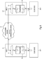
- an optical transceiver 1 can, in a possible embodiment, be plugged into a near end-device 2.
- a looped back optical signal is used for power adjustment.
- the near end-device 2 can be, for example, a transponder for a single client device or a muxponder for multiple client devices.
- the near-end device 2 can for example be also a router, a switch or any other device that can house the optical transceiver 1.
- Such a transponder or muxponder 2 can form part of an add/drop multiplexing node within an optical network.
- the optical span 4 can comprise optical fibers for transmitting an optical signal.
- the far-end device 3 is a passive device with a built-in or integrated unit which can loop back a certain percentage of the optical signal received by the far-end device 3 from the optical transceiver 1 via the optical span 4.
- the optical span 4 comprises two optical fibers 4-1, 4-2 and the integrated loop back unit 5 loops a certain percentage of the optical signal received by the far-end device 3 over the first optical fiber 4-1 via the second optical fiber 4-2 back to the optical transceiver 1.
- the optical transceiver 1 comprises a signal adjustment unit which is adapted to adjust automatically a signal power level of the optical signal transmitted by the optical transceiver 1 via the optical span 4 to the far-end device 3 in response to a determined span loss of the optical span to achieve a predetermined desired receive signal power level of the optical signal received by the far-end device 3.
- the signal adjustment unit integrated in the optical transceiver 1 is a variable optical attenuator.
- the signal adjustment unit integrated in the optical transceiver 1 is a variable gain optical amplifier.
- the loop back unit 5 is integrated in the far-end device 3.
- the loop back unit is integrated in a separate loop back adapter 6.
- the loop back adapter 6 can be connected in the vicinity of the far-end device 3 to the optical span 4 and can comprise an interface of a standard transceiver 7 of the far-end device 3.
- the far-end device 3 can also be formed by a transponder or muxponder for one or several client devices.
- the optical transceiver 1 transmits at least one optical pilot signal via the first fiber 4-1 of said optical span 4 towards the far-end device 3 wherein the optical pilot signal is looped back via the second fiber 4-2 of said optical span 4 to the optical transceiver 1.
- the optical transceiver 1 measures the signal power level of the looped back optical pilot signal received by the optical transceiver 1.
- the span loss of the optical span 4 is determined by the optical transceiver 1 on the basis of the transmit signal power level of the transmitted optical pilot signal transmitted via the first fiber 4-1 and on the basis of the measured receive signal power level of the received looped back optical pilot signal received via the second fiber 4-2.
- the optical pilot signal is looped back by the signal loop back unit which is either formed by a loop adapter 6 as shown in Fig. 1B connected to the optical span 4 at the side of the far-end device 3 or being plugged into the far-end device 3 or integrated into the far-end device 3 as shown in Fig. 1A .
- Attenuation voa Power Tx Near ⁇ End ⁇ EstimatedSpanLoss ⁇ Power Rx Far ⁇ End ⁇ Desired in dB
- the single ended operation for performing an automatic power adjustment in an optical transceiver 1 according to the present invention is correct if the span losses for both fibers 4-1, 4-2 between the near end and the far-end devices are the same. This is true for most applications, because the optical fibers 4-1, 4-2 are arranged within the same strand of optical fibers and undergo the same external influences.
- Fig. 2 shows a diagram for illustrating a further possible embodiment of a method and apparatus for performing an automatic power adjustment according to the present invention.
- a communication channel is used for power adjustment.
- the devices 2, 3, i.e. the near end device 2 as well as the far-end device 3 comprise an optical transceiver 1 according to the present invention.
- the optical transceivers 1-1 and 1-2 can be pluggable transceivers plugged into the respective devices 2, 3.
- the receiver calculates the difference between the received power and the desired received power and sends a message to the other transceiver to adjust the transmit power level by that amount.
- a communication channel can be established via the optical span 4 between both pluggable optical transceivers 1-1, 1-2.
- a communication channel can be formed by an embedded communication channel ECC or by an out of band communication channel.
- the optical transceiver 1-1 can perform the following steps. In a first step, the signal power level of an optical signal received by the optical transceiver 1-1 from the other optical transceiver 1-2 via the optical span 4 is measured an integrated measuring unit of the near end optical transceiver 1-1.
- the measured power level is compared with a predetermined desired receive power level to calculate a difference between the measured received power level and the desired received power level which can be performed by a calculation unit integrated in the near end optical transceiver 1-1.
- the near end optical transceiver 1-1 transmits a power adjustment message via the established communication channel to the other optical transceiver 1-2 to adjust an attenuation or an amplification of the signal power of the optical signal transmitted by the far end optical transceiver 1-2 via the optical span 4 to the near end optical transceiver 1-1.
- the power adjustment message can be transmitted, in a possible embodiment, periodically by the optical transceiver via the established communication channel to the other optical transceiver.
- An advantage of the dual ended operation for performing power adjustment as shown in Fig. 2 over the single ended operation as shown in connection with Figs. 1A, 1B is that in band cross-talk can be avoided.
- a fraction of the signal being looped back at the far-end device 2 towards the transceiver 1 of the near end device 2 may constitute in band crosstalk for the transceiver 1 of the far end device 3 in the direction towards the transceiver 1 of the near end device 2.
- This cross-talk depends on the power levels of the transmitters on both ends of the link, on the span loss in both directions, and on the fraction of the signal being looped back through a splitter/coupler combination of the far-end device.
- a high cross-talk value can degrade a signal performance.
- reducing the amount of looped back signal through selection of a higher ratio of the splitter/coupler pair can reduce the signal power of the optical pilot signal below an acceptable limit for a reliable operation. Accordingly, in the embodiment shown in Figs. 1A, 1B , an optimum signal power for both ends of the link is required to achieve a low cross-talk penalty and a valid optical pilot signal at the same time.
- optical transceiver having an integrated signal adjustment unit such as a variable optical attenuator or a variable gain optical amplifier, a desired balance between low cross-talk and sufficient optical pilot tone signal power can be achieved.
- An advantage of the embodiment shown in Figs. 1A, 1B resides in the fact that no separate communication channel between the optical transceivers has to be established.
- the signal power level of the optical signal is adjusted automatically such that it is balanced with signal power levels of other optical signals transmitted over the same optical span 4 at different wavelengths.
- the signal power level of an optical signal transmitted by the optical transceiver 1 can be adjusted automatically in real time to compensate changes of the transmission capability of the optical span 4. For example, if optical fibers of the optical span 4 are bent, the transmission capability of the span 4 is reduced.
- the signal power level of the optical signal transmitted by the optical transceiver 1 is adjusted automatically in real time to compensate for the reduced transmission capability of the optical span 4 caused by bending the fibers.
- the optical transceiver 1 adapts its transmit power levels until a far-end transceiver receives a flat optimal power level spectrum.
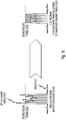
- a WDM optical network there are transmitted signals via different optical channels each having a different wavelength ⁇ .
- Fig. 10A there can be different optical channels transmitting optical signals with different power levels. Some channels have a power level which is beyond a desired receive power level and other optical channels transmit optical signals having signal levels which do not achieve the desired receive power level at the receiving transceiver.
- the near end transceiver adjusts its transmit power levels until a far-end transceiver receives the optimal power level as shown in Fig. 10B.
- Having all the wavelengths of the optical spectrum at the same power level helps to keep the power levels within acceptable limits and also helps to prevent signal degradation caused by the following impairments which can impact the signal performance with improper power levels at the receiver side. If the signal power level is low, the receiver noise is too high at the receiver. If the signal power is high, the receiver may saturate or become overpowered. If the signal power is low at the input of an optical amplifier, the optical signal noise ratio OSNR is low as the amplifier contributes amplified spontaneous emission ASE.
- the optical signal can be distorted due to fiber non-linear effects. Similar effects can occur with high signal power levels, for example in Erbium doped fiber amplifiers or dispersion compensation fiber.
- a large difference in wavelengths powers between adjacent wavelengths ⁇ within an optical spectrum furthermore can generate cross-talk from the high power wavelength ⁇ H to a low power wavelength ⁇ h . This kind of crosstalk can occur in optical filters or optical demultiplexing equipment. For a single ended optical transceiver which utilizes a percentage of the signal looped back towards the transceiver as shown in Figs.
- a high level signal power can result in high levels of cross-talk since the percentage of the signal being transmitted from the near end transceiver is combined on the return signal path with the signal being transmitted from the far-end, i.e. the percentage of the signal transmitted from the near end transceiver becomes cross-talk for the far-end transmitted signal.
- a further advantage of having a flat signal spectrum having all wavelength equalized is that this helps with trouble shooting optical networks as a wavelength power level that is too low or is too high can be easily identified for an equalized spectrum versus an unequalized spectrum when viewing or monitoring the entire optical spectrum. Accordingly, with the method and apparatus according to the present invention, the automatic power adjustment is performed in a preferred embodiment for each optical channel or wavelength ⁇ to achieve a flat receive signal spectrum at the far-end device.
- Fig. 3 shows the use of an optical transceiver 1 according to the present invention wherein the optical transceiver 1 is placed in a router device.
- the optical transceiver 1 is used in a point-to-point connection between a far-end device 3 and a near end device 2.
- the near-end device 3 can be, for example, a router module of a router 8.
- the far-end device 3 in the shown example can be a transponder or muxponder of an optical add/drop multiplexing node 9.
- the optical add/drop multiplexing node 9 can form a node of an optical network such as a DWDM optical network.
- Fig. 4 shows a diagram of an example for an optical network 10.
- the optical network 10 is a node ring network wherein several nodes 1-8 are connected to each other in a ring structure and can perform an add/drop function for adding and dropping channels to/from devices connected to the respective node 1-8.
- the nodes 9-1, 9-2, 9-3, 9-4 are connected with each other over long distance optical fibers wherein each optical node 9-i comprises a network east interface and a network west interface at both sides for connecting to the next two node 9-(i-1), 9-(i+1) of the optical network 10.
- Each network interface can be connected via a corresponding optical fiber pair to a next node.
- the optical network 10 comprises links between the nodes 9-i, each link comprising two optical fibers, wherein each optical fiber pair connects a network west interface of an optical node with a network east interface of the next optical node within the ring.
- the optical signal received by a node 8-i within the optical network can either be dropped at the respective node or pass through to the next node within the ring.
- An optical signal generated by a device connected to the optical node 9-i can be added to the network 10 by means of the node 9-i.
- Fig. 5 shows a block diagram of a possible embodiment of an add/drop multiplexing node 9-i for an optical network 10 according to the present invention.
- the optical network node 9-i comprises a first network interface 11 and a second network interface 12. Both network interfaces 11, 12 are bidirectional interfaces and connect the network node 9-i to the adjacent network nodes 9-(i-1) and 9-(i+1) within the optical network 10.
- the network interfaces 11, 12 are connected to a corresponding multichannel multiplexing/demultiplexing unit 13, 14 comprising a predetermined number of channel ports. In the embodiment shown in Fig. 5 , both multichannel multiplexing/demultiplexing units comprise forty channel ports.
- Both multichannel multiplexing/demultiplexing units 13, 14 comprise an internal optical loop 15, 16 which can reflect a small percentage of an optical signal back towards an optical transceiver.
- both optical network interfaces 11, 12 can comprise an attenuator 17, 18.
- An external fixed attenuator 17, 18 may be installed to adjust pass-through wavelength power levels to locally added wavelengths power levels.
- both ports 39 of the multichannel multiplexing/demultiplexing unit 13, 14 are connected with each other to form a pass through optical channel.
- the attenuators 17, 18 it is possible to adjust the power level of the pass through wavelength of this channel to locally added wavelength power levels.
- some channel ports of the multiplexing/demultiplexing units 13, 14 are connected to transponders or muxponders of the optical node 9-i.
- the first channel port of the first multichannel multiplexing/demultiplexing unit 13 is connected to a transponder 19 provided for a single client device 20 connected to the network node 9-i.
- the client device 20 can for example be a router or a switch.
- the second channel of the first multichannel multiplexing/demultiplexing unit 13 is connected to a muxponder 21 provided for multiple client devices 22-1 to 22-N.
- the last channel 40 of the first multiplexing/demultiplexing unit 13 is again connected to another transponder 19 of a further single client device 20.
- the channels 1, 2 of the second multiplexing/demultiplexing unit 14 are connected by means of transponders 19 to single client devices 20.
- the last channel 40 of the second multiplexing/demultiplexing unit 14 is connected via a muxponder 21 to client devices 22-1 to 22-N performing a group of client devices.
- each multiplexing/demultiplexing unit 13, 14 comprises 40 channel ports.
- the number of channel ports can be higher or lower.
- the number of client devices connectable to one muxponder 21 can vary.
- the muxponder 21 and the transponders 19 can comprise optical transceivers 1 according to the present invention.
- the optical transceivers 1 are connected to a channel port of a multiplexing/demultiplexing unit 13, 14.
- the optical transceiver 1 in a possible embodiment can be plugged into a corresponding transponder 19 or muxponder 21.
- the optical transceivers 1 comprise each a signal adjustment unit adapted to adjust automatically a signal power level of an optical signal transmitted by the respective optical transceiver 1 via an optical span towards the respective channel port of the multichannel multiplexing/demultiplexing unit 13, 14.
- the transmitting optical transceivers 1 comprise a monitoring unit for monitoring at least one optical pilot signal transmitted by the optical transceiver via a first fiber towards the multichannel multiplexing/demultiplexing unit 13, 14 and a looped back via a second fiber to the optical transceiver 1.
- the monitoring unit measures the received signal power level of the looped back optical pilot signal and determines the span loss of the optical span on the basis of the transmitted signal power of the transmitted optical pilot signal and on the basis of the measured received signal power level of the received looped back optical pilot signal.
- the optical pilot signal transmitted by a transceiver is looped back by means of loop back units 15, 16 to reflect a small percentage of the optical signal back towards to the transmitting optical transceiver 1.
- the automatic adjustment of the signal power level is performed in response to a determined span loss of at least one optical span connecting the transceiver with a receiving transceiver.
- An optical span can be formed by the optical connection between a transceiver 1 and the respective channel port of the multiplexing/demultiplexing unit 13, 14 (that may not contain the loop towards the transceiver) and a long distance optical span to a transceiver located in another node of the optical network.
- each optical transceiver 1 thus automatically adjusts a signal power level of an optical signal transmitted by the optical transceiver 1 towards the respective channel port corresponding to a determined span loss to achieve a predetermined desired receive signal power level of the optical signal received by a receiving transceiver within the same or another node. Consequently, different receiving transceivers receive the flat optical power spectrum as shown in Fig. 10B. Since each transponder and muxponder is connected to a multiplexer/demultiplexer, all other channels are filtered out. The flat spectrum is actually experienced on the fiber spans between nodes.
- the optical transceivers 1 connecting the transponders 19 and the muxponders 21 to the channels of the multichannel multiplexing/demultiplexing units 13, 14 are adapted to operate in a single-ended mode as explained in more detail with reference to the embodiments shown in Figs. 1A, 1B .
- Each transponder 19 comprises further an optical transceiver 1' connecting the transponder 19 to a client device 20 such as a router or a switch.
- the client device 20 can comprise a plugged-in optical transceiver 1" being connected to the optical transceiver 1' of the transponder 19 via optical fibers.
- the client device 20 can also be connected directly by means of an optical transceiver 1'' to a multiplexing/demultiplexing unit 13, 14 without going through a transponder or muxponder as illustrated also in Figure 5 .
- the optical transceivers 1', 1" can perform an automatic power adjustment according to the present invention.
- the optical transceiver 1' and 1" can operate in the shown embodiment in a dual-ended mode as explained in more detailed with reference to the embodiment shown in Fig. 2 .
- Fig. 6 shows a diagram for illustrating a dual-ended operation over an optical network using the method and transceiver for performing an automatic power adjustment according to the present invention.
- the transceiver 1 plugged into a transponder 19 of a first optical network node 9-1 turns on a light source such as a laser.
- the optical transceiver 1 transmits an optical signal via multiplexing/demultiplexing units 14 and the optical network 10 to a receiving optical network node 9-2 comprising also a transponder 19 with a plugged-in optical transceiver 1 for operating in a dual-ended node.
- the transceiver 1 within the receiving optical node 9-2 receives the optical signal and measures the power level of the received optical signal.
- the receiving optical transceiver 1 within the receiving node 9-2 calculates the difference between the received signal power level and a predetermined desired receive power level.
- the receiving optical transceiver 1 within the receiving node 9-2 then sends a message to the transmitting optical transceiver 1 within the transmitting node 9-1 indicating the required power adjustment over an established communication channel.
- the transceiver 1 within a transponder 19 of the first optical network node 9-1 receives message from the far-end optical network node 9-2 via the established communication channel.
- a signal adjustment unit integrated in the sending optical transceiver 1 within the first optical node 9-1 adjusts automatically the transmitted power to optimize the far-end receive power level.
- This signal power adjustment can be performed by means of a variable optical attenuator (VOA) or by means of a variable gain optical amplifier.
- VOA variable optical attenuator
- the receiving optical transceiver 1 within the second optical network 9-2 measures, in a further step, the received optical power level which corresponds to the desired optimal power level.
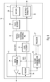
- Fig. 7 shows a block diagram of a possible embodiment of a transponder 19 comprising a pluggable long-reached transceiver 1 and a pluggable short-reached transceiver 1'.
- the pluggable long-reached transceiver 1 comprises a signal adjustment unit 23 being formed by a variable optical attenuator.
- the variable optical attenuator 23 is adapted to adjust automatically a signal power level of an optical signal transmitted by said pluggable long-reached transceiver 1 via one or several optical spans to a far-end device which can be integrated in a far-end optical node of the optical network 10.
- the pluggable long-reach transceiver 1 further can comprise a DWDM transmitter 24 controlled by an in band communication channel control device 25.
- the pluggable long-reach transceiver 1 further comprises a receiver 26 to receive an optical signal from the remote transceiver of the far-end device.
- the communication channel can be formed by an embedded communication channel ECC or by an out of band communication channel.
- the communication channel is provided for transmitting a power adjustment message to the other remote optical transceiver and to receive a power adjustment message from the remote optical transceiver.
- This power adjustment message is received by the receiver 26 via the established communication channel and is extracted by the in band communication channel control unit 25 to be processed by a processor 27 of the transponder 19.
- the processor 27 controls the variable optical attenuator 23 depending on the received power adjustment message.
- the transponder 19 as shown in Fig. 7 can comprise a further pluggable short-reach transceiver 1' for connecting a client device 20 with the transponder 19.
- the pluggable short-reach transceiver 1' comprises a receiver 28 and a short-reach transmitter 29.
- the transponder 19 can further comprise further data processing units for performing a processing of protocol frames or for performance monitoring and forward error correction. These processing units can be integrated into a processing unit 32 as shown in Fig. 7 . For both signal paths of the transponder 19, a clock recovery circuit 30, 31 can be provided.
- Fig. 8 shows a further possible embodiment of a transponder 19 comprising a pluggable long-reach transceiver 1.
- the pluggable long-reach transceiver 1 comprises a variable gain optical amplifier 33 instead of a variable optical attenuator.
- Fig. 9 shows a block diagram of a further possible embodiment of an optical transponder 19.
- the long-reach transceiver is not in the form of a plugged-in device but is integrated in the transponder 19.
- the optical transponder 19 comprises a long-reach interface consisting of discrete transmitter and receiver components and a variable optical attenuator 23.
- the short-reach transceiver 1' of the transponder 19 still forms a pluggable device.
Landscapes
- Engineering & Computer Science (AREA)
- Computer Networks & Wireless Communication (AREA)
- Signal Processing (AREA)
- Physics & Mathematics (AREA)
- Electromagnetism (AREA)
- Optical Communication System (AREA)
Claims (19)
- Verfahren zum Ausführen einer automatischen Leistungsregelung, umfassend:automatisches Regeln eines Signalleistungspegels eines optischen Signals, das durch einen optischen Transceiver (1) über mindestens ein optisches Überbrückungselement (4) zu einer am fernen Ende befindlichen Vorrichtung (3) übertragen wird, in Reaktion auf einen ermittelten Überbrückungselementverlust des optischen Überbrückungselements (4), um einen zuvor festgelegten Soll-Empfangssignalleistungspegel des optischen Signals in der am fernen Ende befindlichen Vorrichtung (3) zu erreichen,wobei eine Signalregelungseinheit in den optischen Transceiver (1) innerhalb eines ersten optischen Knotens eines optischen Netzwerks (10) integriert ist, undwobei der Signalleistungspegel des optischen Signals automatisch so geregelt wird, dass der Signalleistungspegel mit Signalleistungspegeln anderer optischer Signale ausgeglichen wird, die über dasselbe optische Überbrückungselement (4) mit anderen Wellenlängen übertragen werden.
- Verfahren nach Anspruch 1,
wobei mindestens ein optisches Pilotsignal durch den optischen Transceiver (1) über eine erste Faser des optischen Überbrückungselements (4) in Richtung der am fernen Ende befindlichen Vorrichtung (3) übertragen wird und über eine zweite Faser des optischen Überbrückungselements (4) zu dem optischen Transceiver (1) zurückübertragen wird, das den Signalleistungspegel des durch den optischen Transceiver (1) empfangenen zurückübertragenen optischen Pilotsignals misst. - Verfahren nach Anspruch 2, wobei der Überbrückungselementverlust des optischen Überbrückungselements (4) auf der Basis eines Sendesignalleistungspegels des übertragenen optischen Pilotsignals und auf der Basis des gemessenen Empfangssignalleistungspegels des empfangenen zurückübertragenen optischen Pilotsignals ermittelt wird.
- Verfahren nach Anspruch 3, wobei das optische Pilotsignal durch eine Signalrückübermittlungseinheit (5) zurückübertragen wird, die durch einen Schleifenadapter (6) gebildet wird, der mit dem optischen Überbrückungselement (4) auf der Seite der am fernen Ende befindlichen Vorrichtung (3) verbunden ist oder in die am fernen Ende befindliche Vorrichtung (3) eingesteckt ist.
- Verfahren nach Anspruch 1, wobei der Überbrückungselementverlust durch Vergleichen eines gemessenen Signalleistungspegels eines optischen Datensignals, das durch den optischen Transceiver (1) über eine Faser des optischen Überbrückungselements (4) der am fernen Ende befindlichen Vorrichtung (3) empfangen wird, mit einem zuvor festgelegten Soll-Empfangssignalleistungspegel ermittelt wird.
- Verfahren nach Anspruch 5, wobei die am fernen Ende befindliche Vorrichtung (3) ein optischer Transceiver (1) ist und wobei mindestens ein Kommunikationskanal über das optische Überbrückungselement (4) zwischen zwei einsteckbaren optischen Transceivern (1) eingerichtet wird.
- Verfahren nach Anspruch 6, wobei jeder der optischen Transceiver (1) die folgenden Schritte ausführt:- Messen des Signalleistungspegels eines optischen Datensignals, das durch den optischen Transceiver (1) von dem anderen optischen Transceiver (1) über das optische Überbrückungselement (4) empfangen wird,- Vergleichen des gemessenen Signalleistungspegels mit einem zuvor festgelegten Soll-Empfangsleistungspegel zum Berechnen einer Differenz zwischen dem gemessenen Empfangsleistungspegel und dem Soll-Empfangsleistungspegel,- Senden einer Leistungsregelungsmeldung über den eingerichteten Kommunikationskanal an den anderen optischen Transceiver (1) zum Regeln einer Dämpfung oder Verstärkung der Signalleistung des optischen Signals, das durch den anderen optischen Transceiver (1) über das optische Überbrückungselement (4) zu dem optischen Transceiver (1) übertragen wird.
- Verfahren nach Anspruch 6, wobei der eingerichtete Kommunikationskanal von einem eingebetteten Kommunikationskanal oder von einem Außerband-Kommunikationskanal gebildet wird.
- Verfahren nach Anspruch 7, wobei die Leistungsregelungsmeldung periodisch durch den optischen Transceiver (1) über den eingerichteten Kommunikationskanal zu dem anderen optischen Transceiver (1) übertragen wird.
- Verfahren nach Anspruch 1, wobei der Signalleistungspegel des optischen Signals, das durch den optischen Transceiver übertragen wird, automatisch in Echtzeit geregelt wird, um Veränderungen der Übertragungseigenschaften des optischen Überbrückungselements zu kompensieren.
- Optischer Transceiver (1), umfassend:eine Signalregelungseinheit, die dafür ausgelegt ist,einen Signalleistungspegel eines optischen Signals, das durch den optischen Transceiver (1) über mindestens ein optisches Überbrückungselement (4) zu einer am fernen Ende befindlichen Vorrichtung (3) übertragen wird, in Reaktion auf einen ermittelten Überbrückungselementverlust automatisch zu regeln, um einen zuvor festgelegten Soll-Empfangssignalleistungspegel des optischen Signals zu erreichen, das durch die am fernen Ende befindliche Vorrichtung (3) empfangen wird,wobei die Signalregelungseinheit in den optischen Transceiver (1) innerhalb eines ersten optischen Knotens eines optischen Netzwerks (10) integriert ist, und wobei die Signalregelungseinheit so ausgebildet ist, dass der Signalleistungspegel des optischen Signals automatisch so geregelt wird, dass der Signalleistungspegel mit Signalleistungspegeln von anderen optischen Signalen ausgeglichen wird, die über dasselbe optische Überbrückungselement (4) mit anderen Wellenlängen übertragen werden.
- Optischer Transceiver (1) nach Anspruch 11, wobei die Signalregelungseinheit ein variabler optischer Dämpfer oder ein optischer Verstärker mit variabler Verstärkung ist.
- Optischer Transceiver (1) nach Anspruch 11, wobei eine Überwachungseinheit zum Überwachen mindestens eines optischen Pilotsignals vorhanden ist, das durch den optischen Transceiver (1) über eine erste Faser des optischen Überbrückungselements (4) in Richtung der am fernen Ende befindlichen Vorrichtung (3) übertragen und über eine zweite Faser des optischen Überbrückungselements (4) zu dem optischen Transceiver (1) zurückübertragen wird, und
wobei die Überwachungseinheit dafür ausgelegt ist, den Empfangssignalleistungspegel des zurückübertragenen optischen Pilotsignals zu messen, und dafür ausgelegt ist, den Überbrückungselementverlust auf der Basis der Sendesignalleistung des übertragenen optischen Pilotsignals und auf der Basis des gemessenen Empfangssignalleistungspegels des empfangenen zurückübertragenen optischen Pilotsignals zu ermitteln. - Optischer Transceiver (1) nach Anspruch 11, wobei eine Überwachungseinheit vorhanden ist, die dafür ausgelegt ist, die Soll-Leistungsregelung für den am fernen Ende befindlichen Transceiver durch Vergleichen eines gemessenen Signalleistungspegels eines optischen Datensignals, das durch den optischen Transceiver (1) über eine Faser des optischen Überbrückungselements (4) der am fernen Ende befindlichen Vorrichtung (3) empfangen wird, mit einem zuvor festgelegten Soll-Empfangssignalleistungspegel zu ermitteln.
- Optischer Transceiver (1) nach Anspruch 11, wobei die am fernen Ende befindliche Vorrichtung (3) mindestens eine Mehrkanal-Multiplex/Demultiplex-Einheit umfasst, die eine zuvor festgelegte Anzahl von Kanalports umfasst, die jeweils mit einem optischen Transceiver (1) verbunden sind.
- Optischer Transceiver (1) nach Anspruch 11, wobei der optische Transceiver (1) ein einsteckbarer Transceiver ist, der in eine am nahen Ende befindliche Vorrichtung (2) eingesteckt wird und Folgendes umfasst:- einen Transponder für einen einzelnen Client, oder- einen Muxponder für mehrere Clients.
- Optischer Transceiver (1) nach Anspruch 11, wobei der optische Transceiver (1) eine integrierte Steuereinheit zum Generieren eines Steuersignals umfasst, um die Signalregelungseinheit automatisch in Reaktion auf den ermittelten Überbrückungselementverlust des optischen Überbrückungselements (4) zu steuern, oder wobei der optische Transceiver (1) eine Signalregelungseinheit zum Empfangen eines Steuersignals umfasst, um die Signalregelungseinheit automatisch in Reaktion auf den ermittelten Überbrückungselementverlust des optischen Überbrückungselements (4) zu steuern, wobei das empfangene Steuersignal durch eine am nahen Ende befindliche Vorrichtung (2), mit welcher der optische Transceiver (1) verbunden ist, bereitgestellt wird.
- Hinzufügungs-/Abwurf-Multiplexierknoten (9) für ein optisches Netzwerk (10), umfassend:mindestens eine Netzwerkschnittstelle, die mit einer Mehrkanal-Multiplex/Demultiplex-Einheit (13, 14) verbunden ist, die eine zuvor festgelegte Anzahl von Kanalports umfasst, die jeweils mit einem optischen Transceiver (1) verbunden ist, der eine Signalregelungseinheit aufweist, um automatisch einen Signalleistungspegel eines optischen Signals zu regeln, das durch den optischen Transceiver (1) in Richtung des jeweiligen Kanalports übertragen wird, um einen zuvor festgelegten Empfangssignalleistungspegel des optischen Signals bereitzustellen, wobei eine Signalregelungseinheit in den optischen Transceiver (1) innerhalb eines ersten optischen Knotens des optischen Netzwerks (10) integriert ist, undwobei die Signalregelungseinheit so ausgebildet ist, dass der Signalleistungspegel des optischen Signals automatisch so geregelt wird, dass der Signalleistungspegel mit Signalleistungspegeln anderer optischer Signale ausgeglichen wird, die über ein optisches Überbrückungselement, das dasselbe wie das Überbrückungselement des optischen Signals ist, mit anderen Wellenlängen übertragen werden.
- Hinzufügungs-/Abwurf-Multiplexierknoten (9) nach Anspruch 18, wobei die Mehrkanal-Multiplex/Demultiplex-Einheit (13, 14) eine Rückübermittlungseinheit (5) umfasst, die ein optisches Pilotsignal, das durch den optischen Transceiver (1) in Richtung des Kanalports der Multiplex/Demultiplex-Einheit übertragen wird, zu dem optischen Transceiver (1) zurück übermittelt, und
wobei der optische Transceiver (1) einen Überbrückungselementverlust auf der Basis des Sendesignalleistungspegels des übertragenen optischen Pilotsignals und auf der Basis des zurückübertragenen optischen Pilotsignals ermittelt.
Applications Claiming Priority (1)
| Application Number | Priority Date | Filing Date | Title |
|---|---|---|---|
| US12/887,245 US8620156B2 (en) | 2010-09-21 | 2010-09-21 | Method and apparatus for performing an automatic power adjustment for an optical signal |
Publications (2)
| Publication Number | Publication Date |
|---|---|
| EP2432143A1 EP2432143A1 (de) | 2012-03-21 |
| EP2432143B1 true EP2432143B1 (de) | 2017-05-24 |
Family
ID=44999641
Family Applications (1)
| Application Number | Title | Priority Date | Filing Date |
|---|---|---|---|
| EP10195464.2A Active EP2432143B1 (de) | 2010-09-21 | 2010-12-16 | Verfahren und Vorrichtung zum Durchführen einer automatischen Leistungseinstellung für ein optisches Signal |
Country Status (2)
| Country | Link |
|---|---|
| US (2) | US8620156B2 (de) |
| EP (1) | EP2432143B1 (de) |
Families Citing this family (15)
| Publication number | Priority date | Publication date | Assignee | Title |
|---|---|---|---|---|
| US9246580B2 (en) * | 2010-06-24 | 2016-01-26 | Mitsubishi Electric Corporation | Optical add-drop multiplexer (OADM) device |
| US9397754B2 (en) * | 2012-07-25 | 2016-07-19 | Finisar Corporation | Linecards with pluggable interfaces for pluggable optical amplifiers and other pluggable devices |
| CN104521159B (zh) * | 2012-07-31 | 2017-12-15 | 日本电气株式会社 | 波长复用装置和故障发生位置识别方法 |
| US9166722B2 (en) * | 2012-12-12 | 2015-10-20 | Adva Optical Networking Se | Method and apparatus for increasing a transmission performance of a hybrid wavelength division multiplexing system |
| US10481488B2 (en) * | 2012-12-27 | 2019-11-19 | Hoya Corporation | Mask blank substrate processing device, mask blank substrate processing method, mask blank substrate fabrication method, mask blank fabrication method, and transfer mask fabrication method |
| US9608733B2 (en) | 2014-06-09 | 2017-03-28 | Intel Corporation | Optical apparatus with multiple transmission power levels |
| CN106303765B (zh) * | 2015-05-26 | 2019-03-15 | 中兴通讯股份有限公司 | 一种分布式自动功率优化系统及方法 |
| CN106330302B (zh) * | 2015-06-17 | 2019-10-25 | 南京中兴软件有限责任公司 | 一种分布式自动功率优化的方法及装置 |
| EP3579459B1 (de) | 2018-06-06 | 2024-12-18 | Alcatel Submarine Networks | Kommunikationssystem mit verwendung von selbstabstimmenden optischen sendeempfängern |
| US11067478B2 (en) * | 2019-02-05 | 2021-07-20 | Exfo Inc. | Optical loss testing of multi-fiber array cables |
| CN110429984B (zh) * | 2019-09-16 | 2022-12-27 | 广州飞瑞敖电子科技股份有限公司 | 一种用于时分双工模拟光通信系统 |
| TWI731631B (zh) * | 2020-03-23 | 2021-06-21 | 四零四科技股份有限公司 | 在光纖通訊系統內進行動態功率最佳化之方法及相關光纖通訊系統 |
| CN113765583B (zh) * | 2020-06-02 | 2022-12-30 | 华为技术有限公司 | 一种光功率值的传输方法、系统以及相关设备 |
| US20230147398A1 (en) * | 2021-11-05 | 2023-05-11 | Fujitsu Limited | Span loss prediction with federated learning |
| US20240243812A1 (en) * | 2022-11-11 | 2024-07-18 | Infinera Corp. | Systems and methods for optimization of transmission signal quality in point-to-multipoint networks |
Citations (1)
| Publication number | Priority date | Publication date | Assignee | Title |
|---|---|---|---|---|
| WO2001047151A1 (en) * | 1999-12-20 | 2001-06-28 | Sycamore Networks, Inc. | Optical power balancer for optical amplified wdm networks |
Family Cites Families (20)
| Publication number | Priority date | Publication date | Assignee | Title |
|---|---|---|---|---|
| US5225922A (en) * | 1991-11-21 | 1993-07-06 | At&T Bell Laboratories | Optical transmission system equalizer |
| US6563614B1 (en) | 1999-05-21 | 2003-05-13 | Corvis Corporation | Optical transmission system and amplifier control apparatuses and methods |
| US6439777B1 (en) * | 2000-05-15 | 2002-08-27 | Joseph C. Harrison | Fiber optic loop support |
| JP4665344B2 (ja) * | 2001-06-04 | 2011-04-06 | 株式会社日立製作所 | 波長間レベル偏差や光sn偏差を補償する光伝送装置 |
| US20030035203A1 (en) * | 2001-08-09 | 2003-02-20 | Redc Optical Networks Ltd. | Method and apparatus for dynamic optical gain tilting in L-band |
| US7064890B2 (en) | 2001-12-10 | 2006-06-20 | Sumitomo Electric Industries, Ltd. | Optical amplifier and optical communication system including the same |
| IL150347A (en) * | 2002-06-20 | 2008-07-08 | Eci Telecom Ltd | Method and system for span optical power control |
| IL153941A (en) * | 2003-01-14 | 2008-06-05 | Eci Telecom Ltd | Technique for power control in optical networks |
| KR100462029B1 (ko) * | 2003-03-14 | 2004-12-18 | 한국전자통신연구원 | 광섬유 증폭기 및 이의 제어 방법 |
| US7027210B2 (en) | 2003-05-29 | 2006-04-11 | Fujitsu Limited | Method and system for determining gain for an optical signal |
| EP1630984A1 (de) * | 2004-08-30 | 2006-03-01 | Alcatel | Verfahren zur Leistungsregelung eines optischen Verstärkers |
| US7388657B2 (en) * | 2005-08-22 | 2008-06-17 | Tyco Telecommunications (Us) Inc. | System and method for monitoring an optical communication system |
| EP1940050A4 (de) * | 2005-09-21 | 2008-11-19 | Fujitsu Ltd | Überwachungs-steuerlicht-übertragungsverfahren und wellenlängenmultiplex-übertragungseinrichtung in einem wellenlängenmultiplex-übertragungssystem |
| JP4679411B2 (ja) * | 2006-03-31 | 2011-04-27 | 富士通株式会社 | 光通信装置 |
| US7446932B2 (en) * | 2006-06-15 | 2008-11-04 | At&T Corporation | Method, apparatus and system for cost effective optical transmission with fast Raman tilt transient control |
| US8873947B2 (en) * | 2007-09-05 | 2014-10-28 | Alcatel Lucent | Method and apparatus for determining fiber characteristics in an optical communication network |
| CN101911549B (zh) * | 2007-10-22 | 2014-03-05 | 爱立信电话股份有限公司 | 频谱倾斜补偿 |
| EP2071861B1 (de) * | 2007-12-12 | 2014-10-22 | ADVA Optical Networking SE | Verfahren und Netz für bidirektionalen Transport von Daten |
| JP5320973B2 (ja) * | 2008-10-22 | 2013-10-23 | 富士通株式会社 | 光ファイバ伝送路測定装置および光ファイバ伝送路測定システム |
| US8116625B2 (en) | 2009-03-04 | 2012-02-14 | Ciena Coporation | Methods and systems for detecting small span loss changes in fiber optic networks |
-
2010
- 2010-09-21 US US12/887,245 patent/US8620156B2/en not_active Expired - Fee Related
- 2010-12-16 EP EP10195464.2A patent/EP2432143B1/de active Active
-
2013
- 2013-08-29 US US14/014,316 patent/US9397749B2/en active Active
Patent Citations (1)
| Publication number | Priority date | Publication date | Assignee | Title |
|---|---|---|---|---|
| WO2001047151A1 (en) * | 1999-12-20 | 2001-06-28 | Sycamore Networks, Inc. | Optical power balancer for optical amplified wdm networks |
Also Published As
| Publication number | Publication date |
|---|---|
| US9397749B2 (en) | 2016-07-19 |
| US20120070154A1 (en) | 2012-03-22 |
| EP2432143A1 (de) | 2012-03-21 |
| US8620156B2 (en) | 2013-12-31 |
| US20140003809A1 (en) | 2014-01-02 |
Similar Documents
| Publication | Publication Date | Title |
|---|---|---|
| EP2432143B1 (de) | Verfahren und Vorrichtung zum Durchführen einer automatischen Leistungseinstellung für ein optisches Signal | |
| JP5292731B2 (ja) | 光伝送装置 | |
| US7826748B2 (en) | Systems and methods for adaptive gain control to compensate OSNR penalty caused by side-lobe of MEMS-based reconfigurable optical add-drop multiplexers | |
| JP5564692B2 (ja) | 光伝送システム、及び、光ノード | |
| EP0959578B1 (de) | Wellenlängenmultiplexsystem und entsprechender Abschluss | |
| JP4011187B2 (ja) | 光合分波装置 | |
| CN100375416C (zh) | 波分复用光通信系统的插入/分出多路复用器和均衡方法 | |
| EP0924888A2 (de) | Verfahren und Vorrichtung zum Kanalausgleich in Wellenlängen-Multiplex-Systemen | |
| US6904241B2 (en) | Power balanced optical add multiplexer and power balancing methods therefore | |
| JP2009118101A (ja) | 光波長多重伝送装置 | |
| US7081988B2 (en) | Optical amplifier, communication system and method for control tilt of a communication system | |
| US7689131B2 (en) | WDM system | |
| US6885825B2 (en) | Power balanced optical add/drop multiplexer and power balancing methods therefore | |
| EP2903185A1 (de) | Optischer Verstärkungsknoten für ein optisches Raummultiplexnetzwerk | |
| US7512343B2 (en) | Bidirectional communication system | |
| JP2014192615A (ja) | 伝送装置、伝送システム及び光入力パワー制御方法 | |
| JP2012058252A (ja) | ファイバスパンの損失および分散の測定 | |
| JP5909154B2 (ja) | コヒーレント光受信回路及びコヒーレント光受信方法 | |
| JP3589974B2 (ja) | Oadmノード及びそれを用いた波長多重ネットワーク | |
| EP1134925B1 (de) | Optisches Übertragungssystem mit Leistungsoptimierung | |
| US6961525B2 (en) | Method for channel balance | |
| JP4234382B2 (ja) | 光増幅方法、その装置およびその装置を用いた光増幅中継システム | |
| US20040208577A1 (en) | Methods for in-service wavelength upgrade and system performance optimization in WDM optical networks | |
| JP2008503886A (ja) | 波長分割多重(wdm)光分波器 | |
| US20250158708A1 (en) | Optical transmission system, transmission method of optical transmission system, and communication device |
Legal Events
| Date | Code | Title | Description |
|---|---|---|---|
| PUAI | Public reference made under article 153(3) epc to a published international application that has entered the european phase |
Free format text: ORIGINAL CODE: 0009012 |
|
| AK | Designated contracting states |
Kind code of ref document: A1 Designated state(s): AL AT BE BG CH CY CZ DE DK EE ES FI FR GB GR HR HU IE IS IT LI LT LU LV MC MK MT NL NO PL PT RO RS SE SI SK SM TR |
|
| AX | Request for extension of the european patent |
Extension state: BA ME |
|
| 17P | Request for examination filed |
Effective date: 20120921 |
|
| RAP1 | Party data changed (applicant data changed or rights of an application transferred) |
Owner name: ADVA OPTICAL NETWORKING SE |
|
| 17Q | First examination report despatched |
Effective date: 20150601 |
|
| REG | Reference to a national code |
Ref country code: DE Ref legal event code: R079 Ref document number: 602010042531 Country of ref document: DE Free format text: PREVIOUS MAIN CLASS: H04B0010170000 Ipc: H04B0010035000 |
|
| RIC1 | Information provided on ipc code assigned before grant |
Ipc: H04B 10/035 20130101AFI20161221BHEP Ipc: H04J 14/02 20060101ALI20161221BHEP Ipc: H04B 10/079 20130101ALI20161221BHEP Ipc: H04B 10/077 20130101ALI20161221BHEP |
|
| GRAP | Despatch of communication of intention to grant a patent |
Free format text: ORIGINAL CODE: EPIDOSNIGR1 |
|
| STAA | Information on the status of an ep patent application or granted ep patent |
Free format text: STATUS: GRANT OF PATENT IS INTENDED |
|
| INTG | Intention to grant announced |
Effective date: 20170207 |
|
| GRAS | Grant fee paid |
Free format text: ORIGINAL CODE: EPIDOSNIGR3 |
|
| GRAA | (expected) grant |
Free format text: ORIGINAL CODE: 0009210 |
|
| STAA | Information on the status of an ep patent application or granted ep patent |
Free format text: STATUS: THE PATENT HAS BEEN GRANTED |
|
| AK | Designated contracting states |
Kind code of ref document: B1 Designated state(s): AL AT BE BG CH CY CZ DE DK EE ES FI FR GB GR HR HU IE IS IT LI LT LU LV MC MK MT NL NO PL PT RO RS SE SI SK SM TR |
|
| REG | Reference to a national code |
Ref country code: GB Ref legal event code: FG4D |
|
| REG | Reference to a national code |
Ref country code: CH Ref legal event code: EP |
|
| REG | Reference to a national code |
Ref country code: IE Ref legal event code: FG4D |
|
| REG | Reference to a national code |
Ref country code: AT Ref legal event code: REF Ref document number: 896467 Country of ref document: AT Kind code of ref document: T Effective date: 20170615 |
|
| REG | Reference to a national code |
Ref country code: DE Ref legal event code: R096 Ref document number: 602010042531 Country of ref document: DE |
|
| REG | Reference to a national code |
Ref country code: NL Ref legal event code: MP Effective date: 20170524 |
|
| REG | Reference to a national code |
Ref country code: LT Ref legal event code: MG4D |
|
| REG | Reference to a national code |
Ref country code: AT Ref legal event code: MK05 Ref document number: 896467 Country of ref document: AT Kind code of ref document: T Effective date: 20170524 |
|
| PG25 | Lapsed in a contracting state [announced via postgrant information from national office to epo] |
Ref country code: NO Free format text: LAPSE BECAUSE OF FAILURE TO SUBMIT A TRANSLATION OF THE DESCRIPTION OR TO PAY THE FEE WITHIN THE PRESCRIBED TIME-LIMIT Effective date: 20170824 Ref country code: GR Free format text: LAPSE BECAUSE OF FAILURE TO SUBMIT A TRANSLATION OF THE DESCRIPTION OR TO PAY THE FEE WITHIN THE PRESCRIBED TIME-LIMIT Effective date: 20170825 Ref country code: FI Free format text: LAPSE BECAUSE OF FAILURE TO SUBMIT A TRANSLATION OF THE DESCRIPTION OR TO PAY THE FEE WITHIN THE PRESCRIBED TIME-LIMIT Effective date: 20170524 Ref country code: HR Free format text: LAPSE BECAUSE OF FAILURE TO SUBMIT A TRANSLATION OF THE DESCRIPTION OR TO PAY THE FEE WITHIN THE PRESCRIBED TIME-LIMIT Effective date: 20170524 Ref country code: AT Free format text: LAPSE BECAUSE OF FAILURE TO SUBMIT A TRANSLATION OF THE DESCRIPTION OR TO PAY THE FEE WITHIN THE PRESCRIBED TIME-LIMIT Effective date: 20170524 Ref country code: LT Free format text: LAPSE BECAUSE OF FAILURE TO SUBMIT A TRANSLATION OF THE DESCRIPTION OR TO PAY THE FEE WITHIN THE PRESCRIBED TIME-LIMIT Effective date: 20170524 Ref country code: ES Free format text: LAPSE BECAUSE OF FAILURE TO SUBMIT A TRANSLATION OF THE DESCRIPTION OR TO PAY THE FEE WITHIN THE PRESCRIBED TIME-LIMIT Effective date: 20170524 |
|
| PG25 | Lapsed in a contracting state [announced via postgrant information from national office to epo] |
Ref country code: LV Free format text: LAPSE BECAUSE OF FAILURE TO SUBMIT A TRANSLATION OF THE DESCRIPTION OR TO PAY THE FEE WITHIN THE PRESCRIBED TIME-LIMIT Effective date: 20170524 Ref country code: NL Free format text: LAPSE BECAUSE OF FAILURE TO SUBMIT A TRANSLATION OF THE DESCRIPTION OR TO PAY THE FEE WITHIN THE PRESCRIBED TIME-LIMIT Effective date: 20170524 Ref country code: RS Free format text: LAPSE BECAUSE OF FAILURE TO SUBMIT A TRANSLATION OF THE DESCRIPTION OR TO PAY THE FEE WITHIN THE PRESCRIBED TIME-LIMIT Effective date: 20170524 Ref country code: IS Free format text: LAPSE BECAUSE OF FAILURE TO SUBMIT A TRANSLATION OF THE DESCRIPTION OR TO PAY THE FEE WITHIN THE PRESCRIBED TIME-LIMIT Effective date: 20170924 Ref country code: BG Free format text: LAPSE BECAUSE OF FAILURE TO SUBMIT A TRANSLATION OF THE DESCRIPTION OR TO PAY THE FEE WITHIN THE PRESCRIBED TIME-LIMIT Effective date: 20170824 Ref country code: SE Free format text: LAPSE BECAUSE OF FAILURE TO SUBMIT A TRANSLATION OF THE DESCRIPTION OR TO PAY THE FEE WITHIN THE PRESCRIBED TIME-LIMIT Effective date: 20170524 |
|
| PG25 | Lapsed in a contracting state [announced via postgrant information from national office to epo] |
Ref country code: RO Free format text: LAPSE BECAUSE OF FAILURE TO SUBMIT A TRANSLATION OF THE DESCRIPTION OR TO PAY THE FEE WITHIN THE PRESCRIBED TIME-LIMIT Effective date: 20170524 Ref country code: DK Free format text: LAPSE BECAUSE OF FAILURE TO SUBMIT A TRANSLATION OF THE DESCRIPTION OR TO PAY THE FEE WITHIN THE PRESCRIBED TIME-LIMIT Effective date: 20170524 Ref country code: SK Free format text: LAPSE BECAUSE OF FAILURE TO SUBMIT A TRANSLATION OF THE DESCRIPTION OR TO PAY THE FEE WITHIN THE PRESCRIBED TIME-LIMIT Effective date: 20170524 Ref country code: CZ Free format text: LAPSE BECAUSE OF FAILURE TO SUBMIT A TRANSLATION OF THE DESCRIPTION OR TO PAY THE FEE WITHIN THE PRESCRIBED TIME-LIMIT Effective date: 20170524 Ref country code: EE Free format text: LAPSE BECAUSE OF FAILURE TO SUBMIT A TRANSLATION OF THE DESCRIPTION OR TO PAY THE FEE WITHIN THE PRESCRIBED TIME-LIMIT Effective date: 20170524 |
|
| REG | Reference to a national code |
Ref country code: DE Ref legal event code: R097 Ref document number: 602010042531 Country of ref document: DE |
|
| PG25 | Lapsed in a contracting state [announced via postgrant information from national office to epo] |
Ref country code: IT Free format text: LAPSE BECAUSE OF FAILURE TO SUBMIT A TRANSLATION OF THE DESCRIPTION OR TO PAY THE FEE WITHIN THE PRESCRIBED TIME-LIMIT Effective date: 20170524 Ref country code: PL Free format text: LAPSE BECAUSE OF FAILURE TO SUBMIT A TRANSLATION OF THE DESCRIPTION OR TO PAY THE FEE WITHIN THE PRESCRIBED TIME-LIMIT Effective date: 20170524 Ref country code: SM Free format text: LAPSE BECAUSE OF FAILURE TO SUBMIT A TRANSLATION OF THE DESCRIPTION OR TO PAY THE FEE WITHIN THE PRESCRIBED TIME-LIMIT Effective date: 20170524 |
|
| PLBE | No opposition filed within time limit |
Free format text: ORIGINAL CODE: 0009261 |
|
| STAA | Information on the status of an ep patent application or granted ep patent |
Free format text: STATUS: NO OPPOSITION FILED WITHIN TIME LIMIT |
|
| 26N | No opposition filed |
Effective date: 20180227 |
|
| PG25 | Lapsed in a contracting state [announced via postgrant information from national office to epo] |
Ref country code: SI Free format text: LAPSE BECAUSE OF FAILURE TO SUBMIT A TRANSLATION OF THE DESCRIPTION OR TO PAY THE FEE WITHIN THE PRESCRIBED TIME-LIMIT Effective date: 20170524 |
|
| REG | Reference to a national code |
Ref country code: CH Ref legal event code: PL |
|
| REG | Reference to a national code |
Ref country code: IE Ref legal event code: MM4A |
|
| PG25 | Lapsed in a contracting state [announced via postgrant information from national office to epo] |
Ref country code: LU Free format text: LAPSE BECAUSE OF NON-PAYMENT OF DUE FEES Effective date: 20171216 Ref country code: MT Free format text: LAPSE BECAUSE OF NON-PAYMENT OF DUE FEES Effective date: 20171216 |
|
| REG | Reference to a national code |
Ref country code: FR Ref legal event code: ST Effective date: 20180831 |
|
| REG | Reference to a national code |
Ref country code: BE Ref legal event code: MM Effective date: 20171231 |
|
| PG25 | Lapsed in a contracting state [announced via postgrant information from national office to epo] |
Ref country code: IE Free format text: LAPSE BECAUSE OF NON-PAYMENT OF DUE FEES Effective date: 20171216 Ref country code: FR Free format text: LAPSE BECAUSE OF NON-PAYMENT OF DUE FEES Effective date: 20180102 |
|
| PG25 | Lapsed in a contracting state [announced via postgrant information from national office to epo] |
Ref country code: LI Free format text: LAPSE BECAUSE OF NON-PAYMENT OF DUE FEES Effective date: 20171231 Ref country code: CH Free format text: LAPSE BECAUSE OF NON-PAYMENT OF DUE FEES Effective date: 20171231 Ref country code: BE Free format text: LAPSE BECAUSE OF NON-PAYMENT OF DUE FEES Effective date: 20171231 |
|
| PG25 | Lapsed in a contracting state [announced via postgrant information from national office to epo] |
Ref country code: HU Free format text: LAPSE BECAUSE OF FAILURE TO SUBMIT A TRANSLATION OF THE DESCRIPTION OR TO PAY THE FEE WITHIN THE PRESCRIBED TIME-LIMIT; INVALID AB INITIO Effective date: 20101216 Ref country code: MC Free format text: LAPSE BECAUSE OF FAILURE TO SUBMIT A TRANSLATION OF THE DESCRIPTION OR TO PAY THE FEE WITHIN THE PRESCRIBED TIME-LIMIT Effective date: 20170524 |
|
| PG25 | Lapsed in a contracting state [announced via postgrant information from national office to epo] |
Ref country code: CY Free format text: LAPSE BECAUSE OF NON-PAYMENT OF DUE FEES Effective date: 20170524 |
|
| PG25 | Lapsed in a contracting state [announced via postgrant information from national office to epo] |
Ref country code: MK Free format text: LAPSE BECAUSE OF FAILURE TO SUBMIT A TRANSLATION OF THE DESCRIPTION OR TO PAY THE FEE WITHIN THE PRESCRIBED TIME-LIMIT Effective date: 20170524 |
|
| PG25 | Lapsed in a contracting state [announced via postgrant information from national office to epo] |
Ref country code: TR Free format text: LAPSE BECAUSE OF FAILURE TO SUBMIT A TRANSLATION OF THE DESCRIPTION OR TO PAY THE FEE WITHIN THE PRESCRIBED TIME-LIMIT Effective date: 20170524 |
|
| PG25 | Lapsed in a contracting state [announced via postgrant information from national office to epo] |
Ref country code: PT Free format text: LAPSE BECAUSE OF FAILURE TO SUBMIT A TRANSLATION OF THE DESCRIPTION OR TO PAY THE FEE WITHIN THE PRESCRIBED TIME-LIMIT Effective date: 20170524 |
|
| PG25 | Lapsed in a contracting state [announced via postgrant information from national office to epo] |
Ref country code: AL Free format text: LAPSE BECAUSE OF FAILURE TO SUBMIT A TRANSLATION OF THE DESCRIPTION OR TO PAY THE FEE WITHIN THE PRESCRIBED TIME-LIMIT Effective date: 20170524 |
|
| P01 | Opt-out of the competence of the unified patent court (upc) registered |
Effective date: 20230630 |
|
| REG | Reference to a national code |
Ref country code: DE Ref legal event code: R081 Ref document number: 602010042531 Country of ref document: DE Owner name: ADTRAN NETWORKS SE, DE Free format text: FORMER OWNER: ADVA OPTICAL NETWORKING SE, 82152 PLANEGG, DE |
|
| PGFP | Annual fee paid to national office [announced via postgrant information from national office to epo] |
Ref country code: GB Payment date: 20260122 Year of fee payment: 16 |
|
| PGFP | Annual fee paid to national office [announced via postgrant information from national office to epo] |
Ref country code: DE Payment date: 20251229 Year of fee payment: 16 |