EP2436085B1 - Réseau réflecteur à phase variable à faibles pertes utilisant un élément déphaseur à résonance double - Google Patents
Réseau réflecteur à phase variable à faibles pertes utilisant un élément déphaseur à résonance double Download PDFInfo
- Publication number
- EP2436085B1 EP2436085B1 EP10781222.4A EP10781222A EP2436085B1 EP 2436085 B1 EP2436085 B1 EP 2436085B1 EP 10781222 A EP10781222 A EP 10781222A EP 2436085 B1 EP2436085 B1 EP 2436085B1
- Authority
- EP
- European Patent Office
- Prior art keywords
- phase
- reflect array
- shifting elements
- reflector
- array
- Prior art date
- Legal status (The legal status is an assumption and is not a legal conclusion. Google has not performed a legal analysis and makes no representation as to the accuracy of the status listed.)
- Active
Links
Images




Classifications
-
- H—ELECTRICITY
- H01—ELECTRIC ELEMENTS
- H01Q—ANTENNAS, i.e. RADIO AERIALS
- H01Q9/00—Electrically-short antennas having dimensions not more than twice the operating wavelength and consisting of conductive active radiating elements
- H01Q9/04—Resonant antennas
- H01Q9/06—Details
- H01Q9/14—Length of element or elements adjustable
-
- H—ELECTRICITY
- H01—ELECTRIC ELEMENTS
- H01Q—ANTENNAS, i.e. RADIO AERIALS
- H01Q19/00—Combinations of primary active antenna elements and units with secondary devices, e.g. with quasi-optical devices, for giving the antenna a desired directional characteristic
- H01Q19/10—Combinations of primary active antenna elements and units with secondary devices, e.g. with quasi-optical devices, for giving the antenna a desired directional characteristic using reflecting surfaces
- H01Q19/104—Combinations of primary active antenna elements and units with secondary devices, e.g. with quasi-optical devices, for giving the antenna a desired directional characteristic using reflecting surfaces using a substantially flat reflector for deflecting the radiated beam, e.g. periscopic antennas
-
- H—ELECTRICITY
- H01—ELECTRIC ELEMENTS
- H01Q—ANTENNAS, i.e. RADIO AERIALS
- H01Q3/00—Arrangements for changing or varying the orientation or the shape of the directional pattern of the waves radiated from an antenna or antenna system
- H01Q3/44—Arrangements for changing or varying the orientation or the shape of the directional pattern of the waves radiated from an antenna or antenna system varying the electric or magnetic characteristics of reflecting, refracting, or diffracting devices associated with the radiating element
- H01Q3/46—Active lenses or reflecting arrays
Definitions
- This disclosure relates to reflectors for microwave and millimeter wave radiation, in particular to a reflect array and a corresponding method.
- US 2008/024368 A1 relates to a microstrip reflectarray antenna.
- EP 2175523 A1 relates to a reflector array and antenna comprising such a reflector array.
- WO 2007/051487 A1 relates to a reflectarray and a millimetre wave radar.
- OREFICE M ET AL "Analysis of complex circular/square ring reflectarray elements", 3RD EUROPEAN CONFERENCE ON ANTENNAS AND PROPAGATION.
- a passive reflect array is an array of conductive elements adapted to reflect microwave or millimeter wave radiation within a predefined wavelength band.
- the array of conductive elements is typically separated from a continuous ground plane by a thin dielectric layer such that the incident microwave or millimeter wave radiation is reflected by the combined effect of the ground plane and the conductive elements. Since the incident radiation may be reflected with a phase shift that is dependent on the size, shape, or other characteristic of the conductive elements, the term "phase-shifting element" will be used to describe the conductive elements of a reflect array.
- the size, shape, or other characteristic of the phase-shifting elements may be varied to cause a varying phase shift across the extent of the array.
- the varying phase shift may be used to shape or steer the reflected radiation.
- Reflect arrays are typically used to provide a reflector of a defined physical curvature that emulates a reflector having a different curvature.
- a planar reflect array may be used to collimate a diverging microwave or millimeter wave beam, thus emulating a parabolic reflector.
- FIG. 8 shows a graph 800 of data, obtained by simulation, showing the performance of a cross-dipole reflect array as a function of the dipole length dimension L dipole for normally-incident radiation.
- the data summarized in the graph 800 was simulated for a frequency of 95 GHz using specific assumptions for the substrate material, substrate thickness, grid spacing D grid , and dipole width W dipole
- the plotted phase shift is defined as the phase difference between a simulated incident wavefront and a reflected wavefront, both measured at a reference plane displaced from the surface of the reflect array.
- the phase shift data contains a constant phase offset due to the round trip propagation from the reference plane to the reflect array and back.
- the phase shift may be varied from about +105 degrees to +156 degrees (after wrapping through +180 degrees) by varying the dipole length from less than 0.25 mm (10 mils (0.010 inches)) to more than 1.78 mm (70 mils (0.070 inches)).
- the dipole length may be varied from less than 0.25 mm (10 mils (0.010 inches)) to more than 1.78 mm (70 mils (0.070 inches)).
- the inability to achieve a continuously variable phase shift over a 360-degree range may limit the capability of a reflect array to accurately direct and form a reflected beam.
- the simulated reflection loss also varies with the dipole length.
- the reflection loss curve shows a single peak, at a dipole length about 1.07mm (0.042
- the reflection loss peak may occur when the dipole length is equal to one-half of the wavelength of the reflected radiation (including the effect of the dielectric constant of the substrate).
- the reflection loss peak may occur when the length of the dipole is such that the dipole resonates at the wavelength being reflected from the reflect array.
- the dependence of phase shift on the dipole length is strongest in the vicinity of the resonance.
- the phase shift varies substantially when the dipole length is varied from about 0.76 mm (0.03 inch) to about 1.27 mm (0.05 inch), but is relatively constant for dipole lengths less than about 0.76 mm (0.03 inch) or greater than about 1.27 mm (0.05 inch).
- shape is used specifically to describe the form of two-dimensional elements
- curvature is used to describe the form of three-dimensional surfaces.
- curvature may be appropriately applied to flat or planar surfaces, since a planar surface is mathematically equivalent to a curved surface with an infinite radius of curvature.
- solid means unbroken, but does not imply significant depth.
- microwave is used to describe the portions of the radio frequency spectrum above approximately 1 GHz, and thus encompasses the portions of the spectrum commonly called microwave, millimeter wave, and terahertz radiation.
- phase shift is used to describe the change in phase that occurs when a microwave beam is reflected from a surface or device.
- a phase shift is the difference in phase between the reflected and incident beams.
- phase shift will be measured in degrees and defined, by convention, to have a range from -180 degrees to +180 degrees.
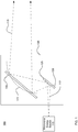
- an exemplary system for generating a beam of microwave energy may include a source of microwave energy 110 and a beam director 120.
- the source of microwave energy 110 may be a solid state source, a vacuum tube source, or another source providing microwave energy.
- the beam director 120 may include one or more beam forming elements such as a primary reflector 130 and a secondary reflector 126.
- the beam director 120 may receive microwave energy 112 from the microwave energy source 110 and may form the received microwave energy 112 into a beam of microwave energy 115.
- the beam of microwave energy 115 shown as a converging beam in FIG. 1 , may be a collimated beam, a diverging beam, or a beam having some other wavefront figure.
- the primary reflector 130 may need to function as an aspheric reflector, as indicated by the dashed shape 124.
- the primary reflector 130 may need to function as an off-axis parabolic reflector.
- the shape of the primary reflector may need to be accurate within a small fraction of a wavelength at a microwave frequency of operation. For example, at a wavelength of 95 GHz, the surface figure of the primary reflector 130 may need to be accurate within a few "25.4 ⁇ m" (thousandths of an inch). This accuracy may be required over a curved shape that may have a diameter of, for example, 0.91 m (3 feet) or larger. Maintaining tight tolerances over a large aspheric shape may greatly increase the cost of an aspheric primary reflector.
- the primary reflector 130 may be a reflect array comprised of an array of conductive phase-shifting elements on a planar substrate. By varying the geometry of the phase-shifting elements across the array, the phase of reflected microwave energy may be varied such that the wavefront reflected from a planar primary reflector 130 is the same as the wavefront reflected from the hypothetical curved reflector 124. In this manner, the planar reflect array 130 may be said to emulate the curved reflector 124.
- the secondary reflector may be a second planar reflect array 126 or a curved reflector as indicated by the curved surface 128.
- the system may or may not fall within the scope of the claims.
- a reflect array 230 not falling within the scope of the claims, which may be suitable for use as the primary reflector 130, may include a two-dimensional array 240 or grid of phase-shifting elements.
- the phase-shifting elements shown in FIG. 2A are uniform, the dimensions and shape of each phase-shifting element may determine the electrical phase shift induced when microwave radiation is reflected from the reflect array.
- the phase-shifting elements may be disposed on a triangular grid, which is to say that the phase-shifting elements in a given row may be laterally offset from the phase-shifting elements in an adjacent row.
- the distance between adjacent rows may be a dimension a.
- the reflect array 230 may be adapted to reflect microwave radiation within a predetermined wavelength band.
- the dimension a may be less than one wavelength, and may be about 0.5 wavelengths, of the microwave radiation in the predetermined frequency band.
- each phase-shifting element such as the phase-shifting element 241 may have a nested hexagon shape including an outer annular hexagonal ring 241a surrounding and concentric with a central hexagonal shape 241b.
- the outer annular hexagonal ring 241a may be characterized by the dimensions R 1 and R 2 , which are the radii of circles that may be drawn through the vertices of the outer and inner hexagons, respectively.
- the central hexagonal shape 241b may be characterized by a dimension R 3 , which is the radius of a circle that may be circumscribed about the shape 241b.
- the phase-shifting elements may have other shapes such as nested circles, nested squares, and other polygonal shapes.
- the reflect array 230 may include a dielectric substrate 232 having a first surface 233 and a second surface 234.
- the dielectric substrate may be a ceramic material, a composite material such as DUROID® (available from Rogers Corporation), or some other dielectric material suitable for use at the frequency of interest.
- the dielectric substrate 232 may have a thickness t.
- the thickness t may be greater or equal to about 1/16 of the free-space wavelength of the predetermined frequency band.
- the thickness t may be less than or equal to 1/4 of the free-space wavelength of the predetermined frequency band.
- the thickness may be about 0.0805 times the free-space wavelength of the predetermined frequency band.
- the thickness t may be 0.25 mm (0.010 inches) for operation at a frequency of 95 GHz.
- the thickness t may vary or may be constant over the extent of the reflect array 230.
- the second surface 234 may support a conductive layer 235.
- the conductive layer 235 may be continuous over all or almost all the second surface 234 and may function as a ground plane.
- the conductive layer 235 may be a thin metallic film deposited onto the second surface 234, or may be a metallic foil laminated to the second surface 234.
- the conductive layer 235 may be a metal element, such as a metal plate that may also function as a structural support and/or heat sink, bonded or otherwise affixed to the second surface 234.
- the first surface 233 may support the array 240 of conductive phase-shifting elements.
- the phase-shifting elements may be formed by patterning a thin metallic film deposited onto the first surface 233, or by patterning a thin metallic foil laminated onto the first surface 233, or by some other method.
- phase-shifting elements shown in FIG. 2A and FIG. 2B are uniform, at least one of the characteristic dimensions R 1 , R 2 , and R 3 of the phase-shifting elements may be varied across the reflect array 230.
- the variation in the dimension of the phase-shifting elements may result in a variation of the phase shift of microwave radiation reflected from specific portions of the reflect array 230.
- a reflect array having a first curvature may be adapted to emulate the optical characteristics of a reflector having a second curvature different from the first curvature.
- a planar reflect array may be adapted to emulate a parabolic reflector, a spherical reflector, a cylindrical reflector, a torroidal reflector, a conic reflector, a generalized aspheric reflector, or some other curved reflector.
- a reflect array having a simple curvature, such as a cylindrical or spherical curvature, may be adapted to emulate a reflector having a complex curvature such as a parabolic reflector, a torroidal reflector, a conic reflector, or a generalized aspheric reflector.
- a graph 300 summarizes simulated performance data for a reflect array not falling within the scope of the claims which incorporates nested hexagonal phase-shifting elements similar to those shown in FIG. 2 .
- the graph 300 shows the dependence of reflection phase shift and reflection loss on the dimension R 1 , which was defined in FIG. 2 .
- the phase shift, in degrees, is shown by a solid line 310.
- the reflection loss, in dB, is shown by a dashed line 320.
- a variable phase reflect array implemented with nested hexagonal- phase-shifting elements can produce any desired phase shift value from - 180 degrees to +180 degrees.
- the dashed line 320 the simulated reflection loss increased rapidly for values of the hexagon radius R 1 greater than about 0.81 mm (0.032 inch). The reflection loss is greater than 0.2 dB when the hexagon radius R 1 is greater than 0.86 mm (0.034 inch).
- phase shift values between +90 degrees and +60 degrees are only achieved, in this example, when the hexagon radius R 1 is greater than 0.86 mm (0.034 inch), which is to say that phase shift values between +90 degrees and +60 degrees are accompanied by relatively high reflection loss.
- the simulated reflection loss has a local peak at R 1 ⁇ 0.50 mm (0.0196") and a second resonance peak (not visible in FIG. 3 ) at R 1 ⁇ 9.04 mm (0.356"), indicating that resonance occurs at two different values of the hexagon radius R 1 .
- Phase-shifting elements that exhibit two resonances, or two loss peaks, as the size of the phase-shifting elements are varied over an allowable range will be referred to as "dual resonance" phase-shifting elements.
- the nested hexagon shapes assumed in this simulation are examples of dual resonance phase-shifting elements.
- the simulated phase shift depends strongly on the hexagon radius R 1 in the vicinity of both resonances. The broad range of phase shown in this simulation may be attributed to the use of dual resonance phase-shifting elements.
- Simulation of the current flowing in the phase-shifting elements indicates that the first resonance, at R 1 ⁇ 0.50 mm (0.0196 inch), may be related to current flowing primarily in the annular hexagon portion of each phase-shifting element.
- the second resonance, at R 1 ⁇ 0.90 mm (0.0356 inch) may be related to current flowing in both the annular hexagon ring and the central solid hexagon shape of each phase-shifting element.
- Similar nested shapes such as nested circles, nested squares, and other polygonal shapes may also exhibit dual resonance and thus be capable of providing a wide range of phase shift values.
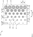
- an array of phase-shifting elements 430 includes a combination of nested hexagon, annular hexagon, and solid hexagon shapes.
- phase-shifting elements 441 and 442 are solid hexagons having an outer radius R 1 of 0.13 mm (0.005 inch) and 0.25 mm (0.010 inch), respectively.
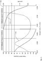
- a graph 500 summarizes simulated performance data for a reflect array which incorporates nested hexagon, annular hexagon, and solid hexagon phase-shifting elements similar to those shown in FIG. 4 .
- the graph 500 shows the dependence of reflection phase shift and reflection loss on the dimension R 1 , which was defined in FIG. 2 .
- the solid line 510 defines the phase shift, in degrees, provided by nested hexagonal phase-shifting elements having R 1 from 0.41 mm (0.016 inch) to 0.86 mm (0.034 inch).
- the dotted line 510A defines the phase shift provided by annular hexagonal phase-shifting elements having R 1 from 0.30 mm (0.012 inch) to 0.41 mm (0.016 inch).
- the dot-dash line 510B defines the phase shift provided by solid hexagonal phase-shifting elements having R 1 from 0 to 0.30 mm (0 to 0.012 inch).
- a variable phase reflect array implemented with a mixture of solid, annular, and nested hexagonal phase-shifting elements may produce any desired phase shift value from -180 degrees to +180 degrees.
- the dashed line 520 defines the reflection loss, in dB, provided by nested hexagonal phase-shifting elements having R 1 from 0.41 mm (0.016 inch) to 0.86 mm (0.034 inch).
- the dotted line 520A defines the reflection loss provided by annular hexagon phase-shifting elements having R 1 from 0.30 mm (0.012 inch) to 0.41 mm (0.016 inch).
- the dot-dash line 520B defines the reflection loss provided by solid hexagon phase-shifting elements having R 1 from 0 to 0.30 mm (0 to 0.012 inch).
- the reflection loss of a variable phase reflect array implemented with a mixture of solid, annular, and nested hexagon phase-shifting elements may be less than about 0.12 dB over the entire range of phase shift values.
- a graph 600 summarizes simulated performance data for another reflect array not falling within the scope of the claims which incorporates nested hexagon and solid hexagon phase-shifting elements similar to those shown in FIG. 4 .
- the graph 600 shows the dependence of reflection phase shift and reflection loss on the dimension R 1 which was defined in FIG. 2 .
- the solid line 610 defines the phase shift, in degrees, provided by nested hexagon phase-shifting elements having R 1 from 0.38 mm (0.015 inch) to 0.81 mm (0.032 inch).
- the dot-dash line 610B defines the phase shift provided by solid hexagon phase-shifting elements having R 1 from 0 to 0.38 mm (0 to 0.015 inch).
- the variable phase reflect array implemented with a mixture of solid and nested hexagon phase-shifting elements may produce any desired phase shift value from -180 degrees to +180 degrees.
- the dashed line 620 defines the reflection loss, in dB, provided by nested hexagon phase-shifting elements having R 1 from 0.38 mm (0.015 inch) to 0.81 mm (0.032 inch).
- the reflection loss of the nested hexagon phase-shifting elements exhibits dual resonance peaks.
- the dot-dash line 620B defines the reflection loss provided by solid hexagon phase-shifting elements having R 1 from 0 to 0.38 mm (0 to 0.015 inch). Similar to the data shown in FIG. 5 , the reflection loss of the variable phase reflect array implemented with a mixture of solid and nested hexagon phase-shifting elements may be less than about 0.125 dB over the entire range of phase shift values.
- FIG. 3 and FIG. 6 show simulation results for two variable phase reflect arrays not falling within the scope of the claims.
- FIG. 5 shows simulation results for an exemplary variable phase reflect array.
- the three simulated reflect arrays are point designs within a continuum of possible designs that may provide variable phase shift over a full 360° range and low reflection loss. Similar results may be obtained for other point designs within the range of dimensions and assumptions used in these three examples.
- FIG. 3 and FIG. 6 show simulation results for two variable- phase reflect arrays not falling within the scope of the claims assuming normally incident microwave energy at a specific frequency of 95 GHz.
- FIG. 5 shows simulation results for an exemplary variable-phase reflect array assuming normally incident microwave energy at a specific frequency of 95 GHz. Similar results may be obtained for non-normal angles of incidence or reflection by suitable choice of physical parameters. These results may extend to other frequencies about 95 GHz, where "about 95 GHz" includes any frequency within the 94 GHz atmospheric radio window. Similar results may be obtained for other frequencies by scaling the assumed physical parameters.
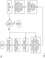
- a process for providing a beam of microwave energy may include generating microwave energy using a source such as microwave energy source 110, and forming the generated microwave energy into a beam of microwave energy, such as microwave energy beam 115, using a beam director such as beam director 120 which may include a dual resonance variable phase reflect array as described herein. Depending on the choice of reflector(s), the process may or may not fall within the scope of the claims.
- the optical performance desired for the reflect array may be defined.
- the defined performance may include converting an incident beam having a first wavefront into a reflected beam having a second wavefront, where the second wavefront is not a specular reflection of the first wavefront.
- the desired performance may also include a definition of an operating wavelength or range of wavelengths, and a maximum reflection loss.
- the reflect array may commonly be a component in a larger system and the desired performance of the reflect array may be defined in conjunction with the other components of the system.
- the required phase shift pattern, or phase shift as a function of position on the reflect array may be calculated from the wavelength and the first and second wavefronts defined at 710.
- the substrate material and thickness may be defined.
- the substrate material and thickness may be defined based upon manufacturing considerations or material availability, or some other basis.
- the grid spacing, phase-shifting element shape, degrees of freedom (how many dimensions that are allowed to vary during the design process), and range of dimensions for the array of phase-shifting elements may be defined. These parameters may be defined by assumption, experience, adaptation of prior designs, other methods, and combinations thereof.
- the reflection phase shift and reflection loss may be calculated by simulating the performance of the reflect array using a suitable simulation tool.
- the degrees of freedom defined at 740 are a selection of three different phase-shifting element shapes (i.e. solid, annular, and nested) and a single variable dimension.
- a plurality of values spanning the full range of the variable dimension may be selected, and the reflection phase shift and reflection loss may be calculated may be calculated for each phase-shifting element shape at all of the values.
- phase-shifting elements may be selected that provide the desired phase shifts at low reflection loss.
- the data from 750 may be graphed as shown in FIGs. 3 , 5 , and 6 , and the appropriate phase-shifting elements may be determined by observation.
- the appropriate phase-shifting elements may also be selected by numerical analysis of the data from 750.
- the performance of the entire reflect array may be simulated and the design may be optimized by adjustment and iteration.
- the simulated performance of the reflect array from 780 may be compared to the optical performance requirements defined at 710. If the design from 780 meets the performance requirements from 710, the process 700 may finish at 795. If the design from 780 does not meet the performance requirements from 710, the process may repeat from steps 710 (changing the optical performance requirements), from 730 (changing the substrate selection), or from 740 (changing the grid spacing, element shapes, degrees of freedom, or range of dimensions) until the optical performance requirements have been satisfied.
- the means are not intended to be limited to the means disclosed herein for performing the recited function, but are intended to cover in scope any means, known now or later developed, for performing the recited function.
- a "set" of items may include one or more of such items.
Landscapes
- Aerials With Secondary Devices (AREA)
Claims (9)
- Réseau réflecteur (130, 230, 430), comprenant
un substrat diélectrique (232) ayant une première surface (233) et une deuxième surface (234),
une couche conductrice (235) supportée par la deuxième surface,
une pluralité d'éléments déphaseurs (240) supportés par la première surface,
les éléments déphaseurs incluant des éléments déphaseurs à double résonance, des éléments déphaseurs hexagonaux annulaires (443), et des éléments déphaseurs hexagonaux pleins (441, 442),
les éléments déphaseurs à double résonance (241) étant des hexagones emboîtés (444, 445, 446) comportant un conducteur interne plein (241b) entouré par un conducteur annulaire concentrique (241a), et un rayon des éléments déphaseurs, représenté par un rayon d'un cercle qui circonscrit l'élément déphaseur, étant soumis à une variation à travers le réseau réflecteur. - Réseau réflecteur de la revendication 1, le déphasage d'un faisceau hyperfréquence (115) réfléchi par le réseau réflecteur étant déterminé, au moins en partie, par au moins une dimension variable des éléments déphaseurs, l'au moins une dimension variable étant un rayon d'un cercle qui circonscrit l'élément déphaseur.
- Réseau réflecteur de la revendication 2, dans lequel
le substrat diélectrique a une première courbure,
la dimension variable est soumise à une variation à travers le réseau réflecteur pour conduire le réseau réflecteur à émuler un réflecteur ayant une deuxième courbure (124) différente de la première courbure. - Réseau réflecteur de la revendication 3, dans lequel
le substrat diélectrique est plan,
le réseau réflecteur émule un réflecteur non plan. - Réseau réflecteur de la revendication 4, le réseau réflecteur émulant un réflecteur incurvé choisi dans le groupe constitué par un réflecteur parabolique, un réflecteur sphérique, un réflecteur cylindrique, un réflecteur toroïdal, un réflecteur conique, et un réflecteur asphérique généralisé.
- Réseau réflecteur de la revendication 3, dans lequel
le substrat diélectrique à une courbure choisie dans le groupe constitué par sphérique et cylindrique,
le réseau réflecteur émule un réflecteur asphérique choisi dans le groupe constitué par un réflecteur parabolique, un réflecteur toroïdal, un réflecteur conique, et un réflecteur asphérique généralisé. - Réseau réflecteur de la revendication 1, dans lequel
une fréquence de fonctionnement du réseau réflecteur est d'environ 95 GHz,
la pluralité d'éléments déphaseurs sont disposés dans un réseau triangulaire,
une distance entre rangées adjacentes du réseau triangulaire est une dimension a, où 1,42 mm < a < 1,65 mm,
une distance entre éléments déphaseurs adjacents dans chaque rangée du réseau triangulaire est une dimension b, où b = 2a cos(30°),
chacun de la pluralité d'éléments déphaseurs est caractérisé par une variable R1 qui est le rayon d'un cercle qui est circonscrit autour de l'élément déphaseur, où R1 < 0,90 mm. - Système (100) destiné à générer un faisceau d'énergie hyperfréquence, comprenant
une source d'énergie hyperfréquence (110),
un dispositif de direction de faisceau (120) pour diriger l'énergie reçue depuis la source d'énergie hyperfréquence en un faisceau d'énergie hyperfréquence (115), le dispositif de direction de faisceau comportant un réseau réflecteur selon une quelconque revendication précédente. - Procédé de génération d'un faisceau d'énergie hyperfréquence, comprenant
la génération d'énergie hyperfréquence,
la formation de l'énergie hyperfréquence en un faisceau avec un dispositif de direction de faisceau, le dispositif de direction de faisceau comportant un réflecteur primaire comprenantun substrat diélectrique (232) ayant une première surface (233) et une deuxième surface (234),une couche conductrice (235) supportée par la deuxième surface,une pluralité d'éléments déphaseurs (240) supportés par la première surface,les éléments déphaseurs incluant des éléments déphaseurs à double résonance, des éléments déphaseurs hexagonaux annulaires (443), et des éléments déphaseurs hexagonaux pleins (441, 442),les éléments déphaseurs à double résonance (241) étant des hexagones emboîtés (444, 445, 446) comportant un conducteur interne plein (241b) entouré par un conducteur annulaire concentrique (241a), et un rayon de l'élément déphaseur, représenté par un rayon d'un cercle qui circonscrit l'élément déphaseur, étant soumis à une variation à travers le réseau réflecteur.
Applications Claiming Priority (2)
| Application Number | Priority Date | Filing Date | Title |
|---|---|---|---|
| US12/475,383 US8149179B2 (en) | 2009-05-29 | 2009-05-29 | Low loss variable phase reflect array using dual resonance phase-shifting element |
| PCT/US2010/036425 WO2010138731A1 (fr) | 2009-05-29 | 2010-05-27 | Réseau réflecteur à phase variable à faibles pertes utilisant un élément déphaseur à résonance double |
Publications (3)
| Publication Number | Publication Date |
|---|---|
| EP2436085A1 EP2436085A1 (fr) | 2012-04-04 |
| EP2436085A4 EP2436085A4 (fr) | 2014-05-14 |
| EP2436085B1 true EP2436085B1 (fr) | 2021-06-23 |
Family
ID=43219630
Family Applications (1)
| Application Number | Title | Priority Date | Filing Date |
|---|---|---|---|
| EP10781222.4A Active EP2436085B1 (fr) | 2009-05-29 | 2010-05-27 | Réseau réflecteur à phase variable à faibles pertes utilisant un élément déphaseur à résonance double |
Country Status (4)
| Country | Link |
|---|---|
| US (1) | US8149179B2 (fr) |
| EP (1) | EP2436085B1 (fr) |
| JP (1) | JP2012528540A (fr) |
| WO (1) | WO2010138731A1 (fr) |
Families Citing this family (13)
| Publication number | Priority date | Publication date | Assignee | Title |
|---|---|---|---|---|
| JP5667887B2 (ja) * | 2011-01-07 | 2015-02-12 | 日本電産エレシス株式会社 | アンテナ装置及びレーダ装置 |
| FR2992780B1 (fr) * | 2012-06-28 | 2016-10-14 | Univ Paris Sud | Antenne a cavite resonante |
| JP6464124B2 (ja) * | 2016-09-08 | 2019-02-06 | 株式会社Soken | アンテナ装置 |
| JP6510394B2 (ja) * | 2015-12-15 | 2019-05-08 | 株式会社Soken | アンテナ装置 |
| WO2017104754A1 (fr) * | 2015-12-15 | 2017-06-22 | 株式会社日本自動車部品総合研究所 | Dispositif antenne |
| US11177577B2 (en) | 2017-02-21 | 2021-11-16 | 3M Innovative Properties Company | Passive repeater device, microwave network, and method of designing a repeater device |
| US11303020B2 (en) * | 2018-07-23 | 2022-04-12 | Metawave Corporation | High gain relay antenna system with multiple passive reflect arrays |
| CN110034413B (zh) * | 2019-05-24 | 2020-10-09 | 电子科技大学 | 一种加载超表面的无遮挡波束偏转天线 |
| US11424549B1 (en) * | 2019-11-27 | 2022-08-23 | Hrl Laboratories, Llc | Wireless coverage control thin film and wireless access system including the same |
| CN113131224B (zh) * | 2020-01-16 | 2022-08-19 | 华为技术有限公司 | 天线波束传播方向调节系统 |
| US11152715B2 (en) | 2020-02-18 | 2021-10-19 | Raytheon Company | Dual differential radiator |
| US20220173521A1 (en) * | 2020-12-02 | 2022-06-02 | Dupont Electronics, Inc. | Telecommunication signal range enhancement using panel reflectance |
| JP7743786B2 (ja) * | 2021-12-24 | 2025-09-25 | Agc株式会社 | 周波数選択表面装荷部材及び車両用窓部材 |
Family Cites Families (19)
| Publication number | Priority date | Publication date | Assignee | Title |
|---|---|---|---|---|
| US4905014A (en) | 1988-04-05 | 1990-02-27 | Malibu Research Associates, Inc. | Microwave phasing structures for electromagnetically emulating reflective surfaces and focusing elements of selected geometry |
| US5153061A (en) * | 1991-01-29 | 1992-10-06 | Westvaco Corporation | Barrier coating to reduce migration of contaminants from paperboard |
| AU1952397A (en) | 1996-01-23 | 1997-08-20 | Malibu Research Associates, Inc. | Dynamic plasma driven antenna |
| SE508356C2 (sv) | 1997-02-24 | 1998-09-28 | Ericsson Telefon Ab L M | Antennanordningar |
| US6020853A (en) | 1998-10-28 | 2000-02-01 | Raytheon Company | Microstrip phase shifting reflect array antenna |
| ES2153323B1 (es) | 1999-06-07 | 2001-07-16 | Univ Madrid Politecnica | Reflectores planos en tecnologia impresa multicapa y su procedimiento de diseño. |
| US6512494B1 (en) * | 2000-10-04 | 2003-01-28 | E-Tenna Corporation | Multi-resonant, high-impedance electromagnetic surfaces |
| US6396449B1 (en) | 2001-03-15 | 2002-05-28 | The Boeing Company | Layered electronically scanned antenna and method therefor |
| US6795020B2 (en) | 2002-01-24 | 2004-09-21 | Ball Aerospace And Technologies Corp. | Dual band coplanar microstrip interlaced array |
| US6900763B2 (en) | 2002-07-11 | 2005-05-31 | Harris Corporation | Antenna system with spatial filtering surface |
| US6885355B2 (en) | 2002-07-11 | 2005-04-26 | Harris Corporation | Spatial filtering surface operative with antenna aperture for modifying aperture electric field |
| US6882460B2 (en) | 2002-08-23 | 2005-04-19 | Energy Conversion Devices, Inc. | Phase angle controlled stationary elements for long wavelength electromagnetic radiation |
| US6744411B1 (en) | 2002-12-23 | 2004-06-01 | The Boeing Company | Electronically scanned antenna system, an electrically scanned antenna and an associated method of forming the same |
| FR2860107B1 (fr) * | 2003-09-23 | 2006-01-13 | Cit Alcatel | Antenne reseau reflecteur reconfigurable a faibles pertes |
| TWM255524U (en) | 2003-12-03 | 2005-01-11 | Tatung Co | Structure of laminated microstrip reflecting-array antenna |
| WO2007051487A1 (fr) | 2005-11-03 | 2007-05-10 | Centre National De La Recherche Scientifique (C.N.R.S.) | Reseau a reflexion et radar a ondes millimetriques |
| TW200807809A (en) | 2006-07-28 | 2008-02-01 | Tatung Co Ltd | Microstrip reflection array antenna |
| US8217847B2 (en) * | 2007-09-26 | 2012-07-10 | Raytheon Company | Low loss, variable phase reflect array |
| FR2936906B1 (fr) | 2008-10-07 | 2011-11-25 | Thales Sa | Reseau reflecteur a arrangement optimise et antenne comportant un tel reseau reflecteur |
-
2009
- 2009-05-29 US US12/475,383 patent/US8149179B2/en active Active
-
2010
- 2010-05-27 WO PCT/US2010/036425 patent/WO2010138731A1/fr not_active Ceased
- 2010-05-27 JP JP2012513258A patent/JP2012528540A/ja active Pending
- 2010-05-27 EP EP10781222.4A patent/EP2436085B1/fr active Active
Non-Patent Citations (1)
| Title |
|---|
| OREFICE M ET AL: "Analysis of complex circular/square ring reflectarray elements", 3RD EUROPEAN CONFERENCE ON ANTENNAS AND PROPAGATION. EUCAP 2009 , 23-27 MARCH 2009 - BERLIN, GERMANY, IEEE, PISCATAWAY, NJ, USA, 23 March 2009 (2009-03-23), pages 1357 - 1359, XP031470040, ISBN: 978-1-4244-4753-4 * |
Also Published As
| Publication number | Publication date |
|---|---|
| EP2436085A1 (fr) | 2012-04-04 |
| JP2012528540A (ja) | 2012-11-12 |
| US20100302120A1 (en) | 2010-12-02 |
| US8149179B2 (en) | 2012-04-03 |
| WO2010138731A1 (fr) | 2010-12-02 |
| EP2436085A4 (fr) | 2014-05-14 |
Similar Documents
| Publication | Publication Date | Title |
|---|---|---|
| EP2436085B1 (fr) | Réseau réflecteur à phase variable à faibles pertes utilisant un élément déphaseur à résonance double | |
| US8217847B2 (en) | Low loss, variable phase reflect array | |
| US7623088B2 (en) | Multiple frequency reflect array | |
| Thornton et al. | Modern lens antennas for communications engineering | |
| US6768468B2 (en) | Reflecting surfaces having geometries independent of geometries of wavefronts reflected therefrom | |
| JP5250764B2 (ja) | レンズアンテナ | |
| Pfeiffer et al. | An UWB hemispherical Vivaldi array | |
| Nguyen et al. | 94 GHz folded Fresnel reflector using C-patch elements | |
| Kedar | Sparse phased array antennas: theory and applications | |
| Sekiguchi et al. | Broadband corrugated horn array with direct machined fabrication | |
| JP4746090B2 (ja) | コリメートされたコヒーレントな波頭を発生するためのミリメートル波トランスリフレクタおよびシステム | |
| Shabbir et al. | A compact single layer reflectarray antenna based on circular delay-lines for X-band applications | |
| US10811787B1 (en) | Systems and methods for wavelength scaled array layout optimization | |
| US6593894B1 (en) | Highly directional receiver and source antennas using photonic band gap crystals | |
| Qasem et al. | Improved Beam Steering Method Using OAM Waves. | |
| Komljenovic et al. | Layered circular-cylindrical dielectric lens antennas—Synthesis and height reduction technique | |
| Foster | Antennas and UWB signals | |
| Hand et al. | Dual-band shared aperture reflector/reflectarray antenna: Designs, technologies and demonstrations for nasa's ACE radar | |
| Suárez et al. | Experimental validation of linear aperiodic array for grating lobe suppression | |
| Elwi et al. | Theory of gain enhancement of UC-PBG antenna structures without invoking Maxwell's equations: An array signal processing approach | |
| Semenikhina et al. | Effect of frequency selective shield of semielliptical shape on the characteristics of antenna array | |
| Caratelli et al. | Design and full-wave analysis of conformal ultra-wideband radio direction finders | |
| Han et al. | Design and performance of a W-band MMW/IR compound Cassegrain antenna system with a hyperbolic sub-reflector based on frequency selective surface | |
| US20240356235A1 (en) | Highly efficient parabolic antenna configured with corrective meta surface structure | |
| Zhang et al. | An OAM antenna with low RCS characteristic based on radiation-scattering-integration strategy |
Legal Events
| Date | Code | Title | Description |
|---|---|---|---|
| PUAI | Public reference made under article 153(3) epc to a published international application that has entered the european phase |
Free format text: ORIGINAL CODE: 0009012 |
|
| 17P | Request for examination filed |
Effective date: 20111213 |
|
| AK | Designated contracting states |
Kind code of ref document: A1 Designated state(s): AL AT BE BG CH CY CZ DE DK EE ES FI FR GB GR HR HU IE IS IT LI LT LU LV MC MK MT NL NO PL PT RO SE SI SK SM TR |
|
| DAX | Request for extension of the european patent (deleted) | ||
| A4 | Supplementary search report drawn up and despatched |
Effective date: 20140414 |
|
| RIC1 | Information provided on ipc code assigned before grant |
Ipc: H01Q 3/46 20060101ALI20140408BHEP Ipc: H01Q 9/14 20060101ALI20140408BHEP Ipc: H01Q 15/00 20060101AFI20140408BHEP Ipc: H01Q 19/10 20060101ALI20140408BHEP |
|
| STAA | Information on the status of an ep patent application or granted ep patent |
Free format text: STATUS: EXAMINATION IS IN PROGRESS |
|
| 17Q | First examination report despatched |
Effective date: 20171018 |
|
| GRAP | Despatch of communication of intention to grant a patent |
Free format text: ORIGINAL CODE: EPIDOSNIGR1 |
|
| STAA | Information on the status of an ep patent application or granted ep patent |
Free format text: STATUS: GRANT OF PATENT IS INTENDED |
|
| INTG | Intention to grant announced |
Effective date: 20201218 |
|
| GRAS | Grant fee paid |
Free format text: ORIGINAL CODE: EPIDOSNIGR3 |
|
| GRAA | (expected) grant |
Free format text: ORIGINAL CODE: 0009210 |
|
| STAA | Information on the status of an ep patent application or granted ep patent |
Free format text: STATUS: THE PATENT HAS BEEN GRANTED |
|
| AK | Designated contracting states |
Kind code of ref document: B1 Designated state(s): AL AT BE BG CH CY CZ DE DK EE ES FI FR GB GR HR HU IE IS IT LI LT LU LV MC MK MT NL NO PL PT RO SE SI SK SM TR |
|
| REG | Reference to a national code |
Ref country code: GB Ref legal event code: FG4D |
|
| REG | Reference to a national code |
Ref country code: CH Ref legal event code: EP |
|
| REG | Reference to a national code |
Ref country code: DE Ref legal event code: R096 Ref document number: 602010067162 Country of ref document: DE Ref country code: AT Ref legal event code: REF Ref document number: 1405113 Country of ref document: AT Kind code of ref document: T Effective date: 20210715 |
|
| REG | Reference to a national code |
Ref country code: IE Ref legal event code: FG4D |
|
| REG | Reference to a national code |
Ref country code: LT Ref legal event code: MG9D |
|
| PG25 | Lapsed in a contracting state [announced via postgrant information from national office to epo] |
Ref country code: FI Free format text: LAPSE BECAUSE OF FAILURE TO SUBMIT A TRANSLATION OF THE DESCRIPTION OR TO PAY THE FEE WITHIN THE PRESCRIBED TIME-LIMIT Effective date: 20210623 Ref country code: LT Free format text: LAPSE BECAUSE OF FAILURE TO SUBMIT A TRANSLATION OF THE DESCRIPTION OR TO PAY THE FEE WITHIN THE PRESCRIBED TIME-LIMIT Effective date: 20210623 Ref country code: BG Free format text: LAPSE BECAUSE OF FAILURE TO SUBMIT A TRANSLATION OF THE DESCRIPTION OR TO PAY THE FEE WITHIN THE PRESCRIBED TIME-LIMIT Effective date: 20210923 Ref country code: HR Free format text: LAPSE BECAUSE OF FAILURE TO SUBMIT A TRANSLATION OF THE DESCRIPTION OR TO PAY THE FEE WITHIN THE PRESCRIBED TIME-LIMIT Effective date: 20210623 |
|
| REG | Reference to a national code |
Ref country code: AT Ref legal event code: MK05 Ref document number: 1405113 Country of ref document: AT Kind code of ref document: T Effective date: 20210623 |
|
| PG25 | Lapsed in a contracting state [announced via postgrant information from national office to epo] |
Ref country code: LV Free format text: LAPSE BECAUSE OF FAILURE TO SUBMIT A TRANSLATION OF THE DESCRIPTION OR TO PAY THE FEE WITHIN THE PRESCRIBED TIME-LIMIT Effective date: 20210623 Ref country code: GR Free format text: LAPSE BECAUSE OF FAILURE TO SUBMIT A TRANSLATION OF THE DESCRIPTION OR TO PAY THE FEE WITHIN THE PRESCRIBED TIME-LIMIT Effective date: 20210924 Ref country code: SE Free format text: LAPSE BECAUSE OF FAILURE TO SUBMIT A TRANSLATION OF THE DESCRIPTION OR TO PAY THE FEE WITHIN THE PRESCRIBED TIME-LIMIT Effective date: 20210623 Ref country code: NO Free format text: LAPSE BECAUSE OF FAILURE TO SUBMIT A TRANSLATION OF THE DESCRIPTION OR TO PAY THE FEE WITHIN THE PRESCRIBED TIME-LIMIT Effective date: 20210923 |
|
| REG | Reference to a national code |
Ref country code: NL Ref legal event code: MP Effective date: 20210623 |
|
| PG25 | Lapsed in a contracting state [announced via postgrant information from national office to epo] |
Ref country code: EE Free format text: LAPSE BECAUSE OF FAILURE TO SUBMIT A TRANSLATION OF THE DESCRIPTION OR TO PAY THE FEE WITHIN THE PRESCRIBED TIME-LIMIT Effective date: 20210623 Ref country code: CZ Free format text: LAPSE BECAUSE OF FAILURE TO SUBMIT A TRANSLATION OF THE DESCRIPTION OR TO PAY THE FEE WITHIN THE PRESCRIBED TIME-LIMIT Effective date: 20210623 Ref country code: SK Free format text: LAPSE BECAUSE OF FAILURE TO SUBMIT A TRANSLATION OF THE DESCRIPTION OR TO PAY THE FEE WITHIN THE PRESCRIBED TIME-LIMIT Effective date: 20210623 Ref country code: SM Free format text: LAPSE BECAUSE OF FAILURE TO SUBMIT A TRANSLATION OF THE DESCRIPTION OR TO PAY THE FEE WITHIN THE PRESCRIBED TIME-LIMIT Effective date: 20210623 Ref country code: ES Free format text: LAPSE BECAUSE OF FAILURE TO SUBMIT A TRANSLATION OF THE DESCRIPTION OR TO PAY THE FEE WITHIN THE PRESCRIBED TIME-LIMIT Effective date: 20210623 Ref country code: RO Free format text: LAPSE BECAUSE OF FAILURE TO SUBMIT A TRANSLATION OF THE DESCRIPTION OR TO PAY THE FEE WITHIN THE PRESCRIBED TIME-LIMIT Effective date: 20210623 Ref country code: PT Free format text: LAPSE BECAUSE OF FAILURE TO SUBMIT A TRANSLATION OF THE DESCRIPTION OR TO PAY THE FEE WITHIN THE PRESCRIBED TIME-LIMIT Effective date: 20211025 Ref country code: NL Free format text: LAPSE BECAUSE OF FAILURE TO SUBMIT A TRANSLATION OF THE DESCRIPTION OR TO PAY THE FEE WITHIN THE PRESCRIBED TIME-LIMIT Effective date: 20210623 Ref country code: AT Free format text: LAPSE BECAUSE OF FAILURE TO SUBMIT A TRANSLATION OF THE DESCRIPTION OR TO PAY THE FEE WITHIN THE PRESCRIBED TIME-LIMIT Effective date: 20210623 |
|
| PG25 | Lapsed in a contracting state [announced via postgrant information from national office to epo] |
Ref country code: PL Free format text: LAPSE BECAUSE OF FAILURE TO SUBMIT A TRANSLATION OF THE DESCRIPTION OR TO PAY THE FEE WITHIN THE PRESCRIBED TIME-LIMIT Effective date: 20210623 |
|
| REG | Reference to a national code |
Ref country code: DE Ref legal event code: R097 Ref document number: 602010067162 Country of ref document: DE |
|
| PG25 | Lapsed in a contracting state [announced via postgrant information from national office to epo] |
Ref country code: DK Free format text: LAPSE BECAUSE OF FAILURE TO SUBMIT A TRANSLATION OF THE DESCRIPTION OR TO PAY THE FEE WITHIN THE PRESCRIBED TIME-LIMIT Effective date: 20210623 |
|
| PLBE | No opposition filed within time limit |
Free format text: ORIGINAL CODE: 0009261 |
|
| STAA | Information on the status of an ep patent application or granted ep patent |
Free format text: STATUS: NO OPPOSITION FILED WITHIN TIME LIMIT |
|
| 26N | No opposition filed |
Effective date: 20220324 |
|
| PG25 | Lapsed in a contracting state [announced via postgrant information from national office to epo] |
Ref country code: AL Free format text: LAPSE BECAUSE OF FAILURE TO SUBMIT A TRANSLATION OF THE DESCRIPTION OR TO PAY THE FEE WITHIN THE PRESCRIBED TIME-LIMIT Effective date: 20210623 |
|
| PG25 | Lapsed in a contracting state [announced via postgrant information from national office to epo] |
Ref country code: IT Free format text: LAPSE BECAUSE OF FAILURE TO SUBMIT A TRANSLATION OF THE DESCRIPTION OR TO PAY THE FEE WITHIN THE PRESCRIBED TIME-LIMIT Effective date: 20210623 |
|
| REG | Reference to a national code |
Ref country code: CH Ref legal event code: PL |
|
| REG | Reference to a national code |
Ref country code: BE Ref legal event code: MM Effective date: 20220531 |
|
| PG25 | Lapsed in a contracting state [announced via postgrant information from national office to epo] |
Ref country code: MC Free format text: LAPSE BECAUSE OF FAILURE TO SUBMIT A TRANSLATION OF THE DESCRIPTION OR TO PAY THE FEE WITHIN THE PRESCRIBED TIME-LIMIT Effective date: 20210623 Ref country code: LU Free format text: LAPSE BECAUSE OF NON-PAYMENT OF DUE FEES Effective date: 20220527 Ref country code: LI Free format text: LAPSE BECAUSE OF NON-PAYMENT OF DUE FEES Effective date: 20220531 Ref country code: CH Free format text: LAPSE BECAUSE OF NON-PAYMENT OF DUE FEES Effective date: 20220531 |
|
| PG25 | Lapsed in a contracting state [announced via postgrant information from national office to epo] |
Ref country code: IE Free format text: LAPSE BECAUSE OF NON-PAYMENT OF DUE FEES Effective date: 20220527 |
|
| PG25 | Lapsed in a contracting state [announced via postgrant information from national office to epo] |
Ref country code: BE Free format text: LAPSE BECAUSE OF NON-PAYMENT OF DUE FEES Effective date: 20220531 |
|
| P01 | Opt-out of the competence of the unified patent court (upc) registered |
Effective date: 20230530 |
|
| PG25 | Lapsed in a contracting state [announced via postgrant information from national office to epo] |
Ref country code: HU Free format text: LAPSE BECAUSE OF FAILURE TO SUBMIT A TRANSLATION OF THE DESCRIPTION OR TO PAY THE FEE WITHIN THE PRESCRIBED TIME-LIMIT; INVALID AB INITIO Effective date: 20100527 |
|
| PG25 | Lapsed in a contracting state [announced via postgrant information from national office to epo] |
Ref country code: MK Free format text: LAPSE BECAUSE OF FAILURE TO SUBMIT A TRANSLATION OF THE DESCRIPTION OR TO PAY THE FEE WITHIN THE PRESCRIBED TIME-LIMIT Effective date: 20210623 Ref country code: CY Free format text: LAPSE BECAUSE OF FAILURE TO SUBMIT A TRANSLATION OF THE DESCRIPTION OR TO PAY THE FEE WITHIN THE PRESCRIBED TIME-LIMIT Effective date: 20210623 |
|
| PG25 | Lapsed in a contracting state [announced via postgrant information from national office to epo] |
Ref country code: TR Free format text: LAPSE BECAUSE OF FAILURE TO SUBMIT A TRANSLATION OF THE DESCRIPTION OR TO PAY THE FEE WITHIN THE PRESCRIBED TIME-LIMIT Effective date: 20210623 |
|
| PG25 | Lapsed in a contracting state [announced via postgrant information from national office to epo] |
Ref country code: MT Free format text: LAPSE BECAUSE OF FAILURE TO SUBMIT A TRANSLATION OF THE DESCRIPTION OR TO PAY THE FEE WITHIN THE PRESCRIBED TIME-LIMIT Effective date: 20210623 |
|
| PGFP | Annual fee paid to national office [announced via postgrant information from national office to epo] |
Ref country code: DE Payment date: 20250423 Year of fee payment: 16 |
|
| PGFP | Annual fee paid to national office [announced via postgrant information from national office to epo] |
Ref country code: GB Payment date: 20250423 Year of fee payment: 16 |
|
| PGFP | Annual fee paid to national office [announced via postgrant information from national office to epo] |
Ref country code: FR Payment date: 20250423 Year of fee payment: 16 |