EP2437100A2 - Display device - Google Patents
Display device Download PDFInfo
- Publication number
- EP2437100A2 EP2437100A2 EP10780717A EP10780717A EP2437100A2 EP 2437100 A2 EP2437100 A2 EP 2437100A2 EP 10780717 A EP10780717 A EP 10780717A EP 10780717 A EP10780717 A EP 10780717A EP 2437100 A2 EP2437100 A2 EP 2437100A2
- Authority
- EP
- European Patent Office
- Prior art keywords
- display panel
- panel
- display
- display device
- superimposed position
- Prior art date
- Legal status (The legal status is an assumption and is not a legal conclusion. Google has not performed a legal analysis and makes no representation as to the accuracy of the status listed.)
- Withdrawn
Links
Images





Classifications
-
- G—PHYSICS
- G06—COMPUTING OR CALCULATING; COUNTING
- G06F—ELECTRIC DIGITAL DATA PROCESSING
- G06F3/00—Input arrangements for transferring data to be processed into a form capable of being handled by the computer; Output arrangements for transferring data from processing unit to output unit, e.g. interface arrangements
- G06F3/01—Input arrangements or combined input and output arrangements for interaction between user and computer
- G06F3/03—Arrangements for converting the position or the displacement of a member into a coded form
- G06F3/041—Digitisers, e.g. for touch screens or touch pads, characterised by the transducing means
- G06F3/0412—Digitisers structurally integrated in a display
-
- G—PHYSICS
- G02—OPTICS
- G02F—OPTICAL DEVICES OR ARRANGEMENTS FOR THE CONTROL OF LIGHT BY MODIFICATION OF THE OPTICAL PROPERTIES OF THE MEDIA OF THE ELEMENTS INVOLVED THEREIN; NON-LINEAR OPTICS; FREQUENCY-CHANGING OF LIGHT; OPTICAL LOGIC ELEMENTS; OPTICAL ANALOGUE/DIGITAL CONVERTERS
- G02F1/00—Devices or arrangements for the control of the intensity, colour, phase, polarisation or direction of light arriving from an independent light source, e.g. switching, gating or modulating; Non-linear optics
- G02F1/01—Devices or arrangements for the control of the intensity, colour, phase, polarisation or direction of light arriving from an independent light source, e.g. switching, gating or modulating; Non-linear optics for the control of the intensity, phase, polarisation or colour
- G02F1/13—Devices or arrangements for the control of the intensity, colour, phase, polarisation or direction of light arriving from an independent light source, e.g. switching, gating or modulating; Non-linear optics for the control of the intensity, phase, polarisation or colour based on liquid crystals, e.g. single liquid crystal display cells
- G02F1/133—Constructional arrangements; Operation of liquid crystal cells; Circuit arrangements
-
- G—PHYSICS
- G02—OPTICS
- G02F—OPTICAL DEVICES OR ARRANGEMENTS FOR THE CONTROL OF LIGHT BY MODIFICATION OF THE OPTICAL PROPERTIES OF THE MEDIA OF THE ELEMENTS INVOLVED THEREIN; NON-LINEAR OPTICS; FREQUENCY-CHANGING OF LIGHT; OPTICAL LOGIC ELEMENTS; OPTICAL ANALOGUE/DIGITAL CONVERTERS
- G02F1/00—Devices or arrangements for the control of the intensity, colour, phase, polarisation or direction of light arriving from an independent light source, e.g. switching, gating or modulating; Non-linear optics
- G02F1/01—Devices or arrangements for the control of the intensity, colour, phase, polarisation or direction of light arriving from an independent light source, e.g. switching, gating or modulating; Non-linear optics for the control of the intensity, phase, polarisation or colour
- G02F1/13—Devices or arrangements for the control of the intensity, colour, phase, polarisation or direction of light arriving from an independent light source, e.g. switching, gating or modulating; Non-linear optics for the control of the intensity, phase, polarisation or colour based on liquid crystals, e.g. single liquid crystal display cells
- G02F1/133—Constructional arrangements; Operation of liquid crystal cells; Circuit arrangements
- G02F1/1333—Constructional arrangements; Manufacturing methods
- G02F1/1335—Structural association of cells with optical devices, e.g. polarisers or reflectors
-
- G—PHYSICS
- G06—COMPUTING OR CALCULATING; COUNTING
- G06F—ELECTRIC DIGITAL DATA PROCESSING
- G06F1/00—Details not covered by groups G06F3/00 - G06F13/00 and G06F21/00
- G06F1/16—Constructional details or arrangements
- G06F1/1613—Constructional details or arrangements for portable computers
- G06F1/1633—Constructional details or arrangements of portable computers not specific to the type of enclosures covered by groups G06F1/1615 - G06F1/1626
- G06F1/1675—Miscellaneous details related to the relative movement between the different enclosures or enclosure parts
-
- G—PHYSICS
- G06—COMPUTING OR CALCULATING; COUNTING
- G06F—ELECTRIC DIGITAL DATA PROCESSING
- G06F1/00—Details not covered by groups G06F3/00 - G06F13/00 and G06F21/00
- G06F1/16—Constructional details or arrangements
- G06F1/1613—Constructional details or arrangements for portable computers
- G06F1/1633—Constructional details or arrangements of portable computers not specific to the type of enclosures covered by groups G06F1/1615 - G06F1/1626
- G06F1/1684—Constructional details or arrangements related to integrated I/O peripherals not covered by groups G06F1/1635 - G06F1/1675
- G06F1/169—Constructional details or arrangements related to integrated I/O peripherals not covered by groups G06F1/1635 - G06F1/1675 the I/O peripheral being an integrated pointing device, e.g. trackball in the palm rest area, mini-joystick integrated between keyboard keys, touch pads or touch stripes
- G06F1/1692—Constructional details or arrangements related to integrated I/O peripherals not covered by groups G06F1/1635 - G06F1/1675 the I/O peripheral being an integrated pointing device, e.g. trackball in the palm rest area, mini-joystick integrated between keyboard keys, touch pads or touch stripes the I/O peripheral being a secondary touch screen used as control interface, e.g. virtual buttons or sliders
-
- H—ELECTRICITY
- H04—ELECTRIC COMMUNICATION TECHNIQUE
- H04M—TELEPHONIC COMMUNICATION
- H04M1/00—Substation equipment, e.g. for use by subscribers
- H04M1/02—Constructional features of telephone sets
- H04M1/0202—Portable telephone sets, e.g. cordless phones, mobile phones or bar type handsets
- H04M1/026—Details of the structure or mounting of specific components
- H04M1/0266—Details of the structure or mounting of specific components for a display module assembly
-
- H—ELECTRICITY
- H05—ELECTRIC TECHNIQUES NOT OTHERWISE PROVIDED FOR
- H05B—ELECTRIC HEATING; ELECTRIC LIGHT SOURCES NOT OTHERWISE PROVIDED FOR; CIRCUIT ARRANGEMENTS FOR ELECTRIC LIGHT SOURCES, IN GENERAL
- H05B33/00—Electroluminescent light sources
- H05B33/02—Details
-
- H—ELECTRICITY
- H10—SEMICONDUCTOR DEVICES; ELECTRIC SOLID-STATE DEVICES NOT OTHERWISE PROVIDED FOR
- H10K—ORGANIC ELECTRIC SOLID-STATE DEVICES
- H10K50/00—Organic light-emitting devices
- H10K50/80—Constructional details
- H10K50/805—Electrodes
- H10K50/82—Cathodes
- H10K50/828—Transparent cathodes, e.g. comprising thin metal layers
-
- H—ELECTRICITY
- H10—SEMICONDUCTOR DEVICES; ELECTRIC SOLID-STATE DEVICES NOT OTHERWISE PROVIDED FOR
- H10K—ORGANIC ELECTRIC SOLID-STATE DEVICES
- H10K59/00—Integrated devices, or assemblies of multiple devices, comprising at least one organic light-emitting element covered by group H10K50/00
- H10K59/80—Constructional details
- H10K59/805—Electrodes
- H10K59/8052—Cathodes
- H10K59/80524—Transparent cathodes, e.g. comprising thin metal layers
-
- G—PHYSICS
- G09—EDUCATION; CRYPTOGRAPHY; DISPLAY; ADVERTISING; SEALS
- G09G—ARRANGEMENTS OR CIRCUITS FOR CONTROL OF INDICATING DEVICES USING STATIC MEANS TO PRESENT VARIABLE INFORMATION
- G09G2300/00—Aspects of the constitution of display devices
- G09G2300/02—Composition of display devices
- G09G2300/023—Display panel composed of stacked panels
-
- G—PHYSICS
- G09—EDUCATION; CRYPTOGRAPHY; DISPLAY; ADVERTISING; SEALS
- G09G—ARRANGEMENTS OR CIRCUITS FOR CONTROL OF INDICATING DEVICES USING STATIC MEANS TO PRESENT VARIABLE INFORMATION
- G09G2360/00—Aspects of the architecture of display systems
- G09G2360/14—Detecting light within display terminals, e.g. using a single or a plurality of photosensors
- G09G2360/144—Detecting light within display terminals, e.g. using a single or a plurality of photosensors the light being ambient light
-
- G—PHYSICS
- G09—EDUCATION; CRYPTOGRAPHY; DISPLAY; ADVERTISING; SEALS
- G09G—ARRANGEMENTS OR CIRCUITS FOR CONTROL OF INDICATING DEVICES USING STATIC MEANS TO PRESENT VARIABLE INFORMATION
- G09G3/00—Control arrangements or circuits, of interest only in connection with visual indicators other than cathode-ray tubes
- G09G3/20—Control arrangements or circuits, of interest only in connection with visual indicators other than cathode-ray tubes for presentation of an assembly of a number of characters, e.g. a page, by composing the assembly by combination of individual elements arranged in a matrix no fixed position being assigned to or needed to be assigned to the individual characters or partial characters
- G09G3/22—Control arrangements or circuits, of interest only in connection with visual indicators other than cathode-ray tubes for presentation of an assembly of a number of characters, e.g. a page, by composing the assembly by combination of individual elements arranged in a matrix no fixed position being assigned to or needed to be assigned to the individual characters or partial characters using controlled light sources
- G09G3/30—Control arrangements or circuits, of interest only in connection with visual indicators other than cathode-ray tubes for presentation of an assembly of a number of characters, e.g. a page, by composing the assembly by combination of individual elements arranged in a matrix no fixed position being assigned to or needed to be assigned to the individual characters or partial characters using controlled light sources using electroluminescent panels
- G09G3/32—Control arrangements or circuits, of interest only in connection with visual indicators other than cathode-ray tubes for presentation of an assembly of a number of characters, e.g. a page, by composing the assembly by combination of individual elements arranged in a matrix no fixed position being assigned to or needed to be assigned to the individual characters or partial characters using controlled light sources using electroluminescent panels semiconductive, e.g. using light-emitting diodes [LED]
- G09G3/3208—Control arrangements or circuits, of interest only in connection with visual indicators other than cathode-ray tubes for presentation of an assembly of a number of characters, e.g. a page, by composing the assembly by combination of individual elements arranged in a matrix no fixed position being assigned to or needed to be assigned to the individual characters or partial characters using controlled light sources using electroluminescent panels semiconductive, e.g. using light-emitting diodes [LED] organic, e.g. using organic light-emitting diodes [OLED]
-
- H—ELECTRICITY
- H04—ELECTRIC COMMUNICATION TECHNIQUE
- H04M—TELEPHONIC COMMUNICATION
- H04M1/00—Substation equipment, e.g. for use by subscribers
- H04M1/02—Constructional features of telephone sets
- H04M1/0202—Portable telephone sets, e.g. cordless phones, mobile phones or bar type handsets
- H04M1/0206—Portable telephones comprising a plurality of mechanically joined movable body parts, e.g. hinged housings
- H04M1/0208—Portable telephones comprising a plurality of mechanically joined movable body parts, e.g. hinged housings characterized by the relative motions of the body parts
- H04M1/0235—Slidable or telescopic telephones, i.e. with a relative translation movement of the body parts; Telephones using a combination of translation and other relative motions of the body parts
-
- H—ELECTRICITY
- H04—ELECTRIC COMMUNICATION TECHNIQUE
- H04M—TELEPHONIC COMMUNICATION
- H04M2250/00—Details of telephonic subscriber devices
- H04M2250/16—Details of telephonic subscriber devices including more than one display unit
-
- H—ELECTRICITY
- H04—ELECTRIC COMMUNICATION TECHNIQUE
- H04M—TELEPHONIC COMMUNICATION
- H04M2250/00—Details of telephonic subscriber devices
- H04M2250/22—Details of telephonic subscriber devices including a touch pad, a touch sensor or a touch detector
-
- H—ELECTRICITY
- H10—SEMICONDUCTOR DEVICES; ELECTRIC SOLID-STATE DEVICES NOT OTHERWISE PROVIDED FOR
- H10K—ORGANIC ELECTRIC SOLID-STATE DEVICES
- H10K2102/00—Constructional details relating to the organic devices covered by this subclass
- H10K2102/301—Details of OLEDs
- H10K2102/302—Details of OLEDs of OLED structures
- H10K2102/3023—Direction of light emission
- H10K2102/3031—Two-side emission, e.g. transparent OLEDs [TOLED]
-
- H—ELECTRICITY
- H10—SEMICONDUCTOR DEVICES; ELECTRIC SOLID-STATE DEVICES NOT OTHERWISE PROVIDED FOR
- H10K—ORGANIC ELECTRIC SOLID-STATE DEVICES
- H10K59/00—Integrated devices, or assemblies of multiple devices, comprising at least one organic light-emitting element covered by group H10K50/00
- H10K59/40—OLEDs integrated with touch screens
Definitions
- display devices applied to mobile communication terminals include a Liquid Crystal Display (LCD), an Organic Light Emitting Diode (OLED), and Electronic-paper (E-paper).
- LCD Liquid Crystal Display
- OLED Organic Light Emitting Diode
- E-paper Electronic-paper
- the display device including the main display panel and the sub display panel has an advantage of low power consumption compared with the full-touch functional display device but has the disadvantage of being structurally limited because a separate arrangement space is necessary to include the sub display panel. Therefore, a technique is required to minimize the thickness of the sub display panel so that the entire display device can be slim and compact.
- the TOLED panel includes: a substrate; a first electrode formed on the substrate; an organic layer formed on the first electrode; a second electrode formed on the organic layer; and a transparent layer formed between the organic layer and the second electrode and/or on the second electrode, and configured to include any one selected from a group consisting of oxides, nitrides, salts, and mixtures thereof.
- the oxides comprise MoO 3 , ITO, IZO, 10, ZnO, TO, TiO 2 , SiO 2 , WO 3 , AL 2 O 3 , Cr 2 O 3 , TeO 2 and SrO 2 .
- the salts include Cs 2 CO 3 , Li 2 CO 3 , K 2 CO 3 , Na 2 CO 3 , LiF, CsF, and ZnSe.
- the organic layer includes an electron transporting layer doped with any one selected from a group consisting of low-work-function metals and mixtures thereof in order to facilitate injection of electrons from the second electrode.
- the OLED panel is the self luminous phenomenon in which electrons and holes (particles each having an electric charge corresponding to electron) injected from cathode and anode are electrically combined with each other in organic matter, thereby emitting light, or is an organic light-emitting diode which uses the self luminous phenomenon. Since the OLED panel can be understood using well-known techniques, the detailed description thereof will be omitted.
- the function of the second embodiment is implemented by a signal detected from one of the second touch panels 54, which is rotated relatively to the first touch panel 52, in the non-superimposed position of the first display panel 12 and the second display panel 14,.
- the first transparent layer 191 may be formed between the electron injection layer 179 and second electrode 150 of the organic layer 170, or may be formed in the electron injection layer 179 itself.
- the second transparent layer 192 may be placed on the top surface of the second electrode 150 which faces the first transparent layer 191.
- the oxides may include MoO 3 , ITO, IZO, IO, ZnO, TO, TiO 2 , SiO 2 , WO 3 , Al 2 O 3 , Cr 2 O 3 , TeO 2 and SrO 2 .
- the nitrides may include Si 3 N 4 and AIN.
- the salts may include Cs 2 CO 3 , Li 2 CO 3 , K 2 CO 3 , Na 2 CO 3 , LiF, CsF and ZnSe.
- the transparent layer 190 when the thickness of the transparent layer 190 is equal to or greater than 100 nm, the performance is not deteriorated due to decrease in resistance, but the transmittance decreases due to increase in the thickness of the transparent layer 190. Meanwhile, it is preferred that the transparent layer 190 according to the embodiment of the present invention be formed using thermal evaporation.
Landscapes
- Engineering & Computer Science (AREA)
- Physics & Mathematics (AREA)
- Theoretical Computer Science (AREA)
- General Engineering & Computer Science (AREA)
- General Physics & Mathematics (AREA)
- Computer Hardware Design (AREA)
- Human Computer Interaction (AREA)
- Nonlinear Science (AREA)
- Optics & Photonics (AREA)
- Crystallography & Structural Chemistry (AREA)
- Chemical & Material Sciences (AREA)
- Mathematical Physics (AREA)
- Signal Processing (AREA)
- Electroluminescent Light Sources (AREA)
- Control Of Indicators Other Than Cathode Ray Tubes (AREA)
- Devices For Indicating Variable Information By Combining Individual Elements (AREA)
- Liquid Crystal (AREA)
- Control Of El Displays (AREA)
- Digital Computer Display Output (AREA)
- Liquid Crystal Display Device Control (AREA)
- Position Input By Displaying (AREA)
Abstract
Description
- The present invention relates generally to a display device, and, more particularly, to a display device for separately displaying information on the display panels of a dual display panel in response to a signal detected from a touch panel.
- Recently, display devices for displaying various types of information are applied to both large-sized electronic equipment, such as Televisions (TV), and small-sized electronic equipment, such as Portable Media Players (PMP), Moving Picture Experts Group Audio Layer-3 (MP3), and mobile phones.
- In particular, display devices applied to mobile communication terminals, such as mobile phones, include a Liquid Crystal Display (LCD), an Organic Light Emitting Diode (OLED), and Electronic-paper (E-paper).
- Meanwhile, in the recent industrial trend for such a display device, a touch panel is used as an input manner of applying signals in order to display information on the display device. The display device having a touch panel is divided into a full-touch functional display device including a single display panel and a touch panel, and a display device including a touch panel, a main display panel, and a sub display panel in order to reduce power consumption.
- Here, the sub display panel displays simple sub information, such as the remaining battery capacity, the current time, the date, and a user's name.
- However, the display device including the main display panel and the sub display panel has an advantage of low power consumption compared with the full-touch functional display device but has the disadvantage of being structurally limited because a separate arrangement space is necessary to include the sub display panel. Therefore, a technique is required to minimize the thickness of the sub display panel so that the entire display device can be slim and compact.
- Further, the function of the sub display panel for displaying the above-described simple sub information, such as the remaining battery capacity, the current time, the date, and a user's name, requires improving. That is, in order to increase the convenience to users, the necessity for a dual-type display device for separately displaying information on a main display panel and on a sub display panel in response to a signal detected from a touch panel has been on the rise.
- Accordingly, the present invention has been made keeping in mind the above problems occurring in the prior art, and an object of the present invention is to provide a display device which makes improvements in spatial limitations in order to include a separate sub display panel, so that the display device can be slim and compact.
- Another object of the present invention is to provide a display device which makes improvements in the structure and control method thereof in order to drive two display panels separately in response to a signal detected from a touch panel.
- In order to accomplish the above object, the present invention provides a display device including: a first display panel configured to display first information; a second display panel selectively placed in a superimposed position, in which the second display panel is superimposed on the first display panel, and in a non-superimposed position, in which the second display panel is not superimposed on the first display panel, and configured to display second information; a first touch panel disposed on the first display panel; one or more second touch panels disposed on the second display panel or disposed on both side surfaces of the second display panel in pairs; and a control unit configured to apply driving voltage to at least one of the first and second display panels based on a signal detected from at least one of the first and second touch panels depending on any one of the superimposed position and the non-superimposed position of the first and second display panels.
- Here, the first display panel includes an Organic Light-Emitting Diode (OLED) panel.
- The first display panel includes any one of a Liquid Crystal Display (LCD) panel and Electronic-paper (E-Paper).
- Further, the second display panel includes an OLED panel.
- The OLED panel includes a Transparent Organic Light-Emitting Diode (TOLED) panel.
- The TOLED panel includes: a substrate; a first electrode formed on the substrate; an organic layer formed on the first electrode; a second electrode formed on the organic layer; and a transparent layer formed between the organic layer and the second electrode and/or on the second electrode, and configured to include any one selected from a group consisting of oxides, nitrides, salts, and mixtures thereof. Here, the oxides comprise MoO3, ITO, IZO, 10, ZnO, TO, TiO2, SiO2, WO3, AL2O3, Cr2O3, TeO2 and SrO2.
- The nitrides include Si3N4 and AIN.
- The salts include Cs2CO3, Li2CO3, K2CO3, Na2CO3, LiF, CsF, and ZnSe.
- The thickness of the transparent layer is equal to or greater than 0.1 nm and less than 100 nm.
- The organic layer includes an electron transporting layer doped with any one selected from a group consisting of low-work-function metals and mixtures thereof in order to facilitate injection of electrons from the second electrode.
- The low-work-function metals include Cs, Li, Na, K, and Ca.
- The mixtures thereof include Li-Al, LiF, CsF, and Cs2CO3.
- Preferably, the TOLED panel exhibits a transmittance ranging from 70 to 99% depending on wavelength (nm).
- The second display panel moves on the first display panel in a sliding manner between the superimposed position and the non-superimposed position. Preferably, the control unit applies the driving voltage to the first display panel based on the signal detected from the second touch panel when the first and second display panels are placed in the superimposed position. Meanwhile, the control unit applies the driving voltage to the first display panel based on the signal detected from the first touch panel and applies the driving voltage to the second display panel based on the signal detected from the second touch panel when the first and second display panels are placed in the non-superimposed position. A brightness measurement sensor for detecting intensity of an outside illumination is further included, and the control unit controls the driving voltage based on a signal detected from the brightness measurement sensor so that the brightness of any one of the first and second display panels is adjusted. In order to accomplish the above object, the present invention provides a display device including: a first display panel configured to display first information; a second display panel selectively placed in a superimposed position, in which the second display panel is superimposed on the first display panel, and a non-superimposed position, in which the second display panel is not superimposed on the first display panel, and configured to display second information; a touch panel disposed on the second display panel; and a control unit configured to, when the first and the second display panels are placed in any one of the superimposed position and the non-superimposed position, selectively apply driving voltage to the first and second display panels based on a signal detected from the touch panel. Here, the first display panel includes any one of an OLED panel, an LCD panel, and E-Paper; and the second display panel comprises the OLED panel. Further, the OLED panel includes a TOLED panel. The second display panel moves on the first display panel in a sliding manner between the superimposed position and the non-superimposed position. The second display panel moves relative to the first display panel in a rotating manner between the superimposed position and the non-superimposed position. The control unit applies the driving voltage to the first display panel based on the signal detected from the touch panel when the first and second display panels are placed in the superimposed position. Meanwhile, the control unit applies the driving voltage to the second display panel based on the signal detected from the touch panel when the first and second display panels are placed in the non-superimposed position. A brightness measurement sensor for detecting intensity of an outside illumination is further included, and the control unit controls the driving voltage based on a signal detected from the brightness measurement sensor so that brightness of at least any one of the first and second display panels is adjusted.
- Further, in order to accomplish the above object, the present invention provides a display device including: a first display panel configured to display first information; a second display panel selectively placed in a superimposed position, in which the second display panel is superimposed on the first display panel, and a non-superimposed position, in which the second display panel is not superimposed on the first display panel, and configured to display second information; a first touch panel disposed on the first display panel; a second touch panel disposed on one surface of the second display panel which is rotated relatively to the first touch panel; and a control unit configured to selectively apply driving voltage to the first and second display panels based on a signal detected from the first or second touch panels.
- The first display panel includes any one of an OLED panel, an LCD panel, and E-paper; and the second display panel includes the OLED panel.
- The OLED panel includes a TOLED panel.
- The second display panel moves on the first display panel in a sliding manner between the superimposed position and the non-superimposed position.
- Meanwhile, the second display panel moves relative to the first display panel in a rotating manner between the superimposed position and the non-superimposed position.
- Preferably, the control unit applies the driving voltage to the first display panel based on the signal detected from the first touch panel and applies the driving voltage to the second display panel based on the signal detected from the second touch panel when the first and second display panels are placed in the non-superimposed position.
- A brightness measurement sensor for detecting intensity of an outside illumination is further included, and the control unit controls the driving voltage based on a signal detected from the brightness measurement sensor so that brightness of any one of the first and second display panels is adjusted.
- Therefore, according to the invention, a TOLED panel is used as any one of display panels of the dual display panel, so that the display device which is slim and compact is provided.
- Further, each of the display panels of the dual display panel includes a touch panel, and the display panels are connected to be mutually moved, so that different information can be displayed on the separate display panels, thereby increasing the use of the product.
- Furthermore, information is separately displayed on different display panels depending on the superimposed position and non-superimposed position of the dual display panel, thereby increasing the use of the product.
- Further, in the a TOLED panel used as the display panel, the transparent layer which is made of any one selected from a group consisting of oxides, nitrides, salts, and the mixtures thereof is formed between the organic layer and the second electrode or formed on the top of the second electrode, so that a display device capable of realizing double-sided light emission and improving transmittance is provided.
- The transparent layer is made of any one selected from a group consisting of oxides, nitrides, salts, and the mixtures thereof, so that the increase in the internal resistance of the second electrode can be prevented, thereby improving transmittance and electrical performance of products.
-
-
FIG. 1 is block diagram showing the control of a display device according to an embodiment of the present invention; -
FIG. 2 is a perspective view showing a display device according to a first embodiment of the present invention; -
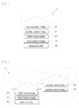
FIG. 3 is a schematic view showing a structure in which the first display panel and second display panel of the display device according to the first embodiment of the present invention are in a superimposed position; -
FIG. 4 is a schematic view showing a structure in which the second display panel moves on the first display panel in a sliding manner, the second display panel and the first display panel being shown inFIG. 3 ; -
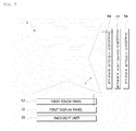
FIG. 5 is a schematic view showing a structure in which a second display panel moves against a first display panel in a rotating manner, the second display panel and the first display panel being included in a display device according to a second embodiment of the present invention; -
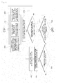
FIG. 6 is a flowchart showing the control of the display device according to the first and second embodiments of the present invention; -
FIG. 7 is a schematic view showing a structure in which a second display panel moves against a first display panel in a rotating manner, the second display panel and the first display panel being included in a display device according to a third embodiment of the present invention; -
FIG. 8 is a flowchart showing the control of the display device according to the third embodiment of the present invention; -
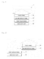
FIG. 9 is a schematic view showing a structure in which the first display panel and second display panel of a display device according to a fourth embodiment of the present invention are in a superimposed position; -
FIG. 10 is a schematic view showing a structure in which the second display panel moves on the first display panel in a sliding manner, the second display panel and the first display panel being shown inFIG. 9 ; -
FIG. 11 is a flowchart showing the control of the display device according to the fourth embodiment of the present invention; -
FIG. 12 is a view showing the cross section of the second display panel according to the embodiment of the present invention; -
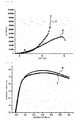
FIG. 13 is a graph showing transmittance of the transparent layer of the second display panel ofFIG. 12 ; -
FIG. 14 is a graph showing luminance of the transparent layer of the second display panel ofFIG. 12 ; and -
FIG. 15 is a graph showing transmittance when a transparent layer is formed of any one selected from a group consisting of oxides, salts, and mixtures thereof on the second display panel ofFIG. 12 . -
10 : display panel 12 : first display panel 12' : first display panel 14 : second display panel 14' : second display panel 50: touch panel 52 : first touch panel 54 : second touch panel 70 : brightness measurement sensor 90 : control unit 100 : substrate 130 : first electrode 150 : second electrode 170 : organic layer 172 : Hole Injection Layer 174 : Hole Transporting Layer 176 : Emissive Layer 178 : Electron Transporting Layer 179 : Electron Injection Layer 190 : transparent layer 191 : first transparent layer 192 : second transparent layer - A display device according to an embodiment of the present invention will be described in detail below by referring to the accompanying drawings.
- Before the description, when it is determined that the detailed descriptions of well-known techniques related to the present invention or detailed description of construction in the embodiment of the present invention would obscure the gist of the present invention, they will be omitted.
- Further, it is noted that, in the first to fourth embodiments of the present invention, different reference numerals are used for a first display panel and a second display panel in the first to third embodiments in which a plurality of touch panels are used and in the fourth embodiment in which a single touch panel is used.
- Further, it is noted that the same reference numeral is used for a second touch panel through the first to third embodiments of the present invention regardless of the arrangement location and arrangement number thereof.
-
FIG. 1 is block diagram showing the control of a display device according to the first to fourth embodiments of the present invention. Although the touch panel and display panel ofFIG. 1 comprehensively implement the first to fourth embodiments of the present invention, the detailed description thereof will be separately performed. - As shown in
FIG. 1 , thedisplay device 1 according to the embodiments of the present invention includes adisplay panel 10, atouch panel 50, abacklight unit 30, abrightness measurement sensor 70, and acontrol unit 90. - The
display panel 10 of thedisplay device 1 according to a first embodiment of the present invention includes afirst display panel 12, asecond display panel 14, and adriver IC 16, as shown inFIG. 2 . - Any one of an Organic Light-Emitting Diode (OLED) panel, a liquid crystal display (LCD) panel and Electronic paper (E-paper) is used as the
first display panel 12. - The OLED panel, used as the
first display panel 12, will be described in detail when thesecond display panel 14 will be described. Hereinafter, thefirst display panel 12 which employs a liquid crystal panel or E-paper will be described. - A liquid crystal panel, used as the
first display panel 12, displays characters, numbers, and icons by selectively passing light, radiated from thebacklight unit 30 provided under thefirst display panel 12, using dielectric anisotropy in which the alignment direction of liquid crystal changes depending on voltage applied from outside. Thebacklight unit 30 includes a Cold Cathode Fluorescent Lamp (CCFL), an External Electrode Fluorescent Lamp (EEFL), a Light-Emitting Diode (LED), and a Flat Fluorescent Lamp (FFL). Since the liquid crystal panel can be understood using well-known techniques, the detailed description thereof will be omitted. - E-paper, used as the
first display panel 12, uses the characteristics of ordinary ink on paper. E-paper displays information using reflection light like ordinary paper. Since the E-paper can be understood using well-known techniques like the liquid crystal panel, the detailed description thereof will be omitted. - A liquid crystal panel is used as the
first display panel 12 of thedisplay device 1 according to the embodiment of the present invention from between the liquid crystal panel and the E-paper. Of course, since the liquid crystal panel is used as thefirst display panel 12, thebacklight unit 30 for radiating light is mounted on one side of thefirst display panel 12. - A driving Integrated Circuit (IC) 16a for the first display panel, which is electrically connected to the
control unit 90 which will be described later, is mounted on thefirst display panel 12. First information is displayed on thefirst display panel 12 in such a way that thedriver IC 16a for the first display panel is operated under the control of thecontrol unit 90. Here, the first information is referred to as main information. Therefore, it can be understood that thefirst display panel 12 is used as a main display panel. For example, when thefirst display panel 12 is applied to a mobile communication terminal, such as a mobile phone, and portable equipment, such as a PMP, thefirst display panel 12 displays characters, numbers, icons, and moving pictures, the resolution of which is higher than that of information to be displayed on asecond display panel 14 which will be described later. - An OLED panel is used as the
second display panel 14. The OLED panel is the self luminous phenomenon in which electrons and holes (particles each having an electric charge corresponding to electron) injected from cathode and anode are electrically combined with each other in organic matter, thereby emitting light, or is an organic light-emitting diode which uses the self luminous phenomenon. Since the OLED panel can be understood using well-known techniques, the detailed description thereof will be omitted. - The
second display panel 14 of the present invention includes a Transparent Organic Light Emitting Diode (TOLED) panel of the OLED panel. The TOLED panel is a transparent OLED panel manufactured by coating a hole transporting layer, an emissive layer, and an electron transporting layer on the transparent positive electrode of Indium-Tin Oxide (ITO), thinly coating a transparent negative electrode thereon, and coating an ITO film used for compensating for conductivity, functioning as a protection layer, and maintaining transparency thereon. As shown inFIG. 3 , the TOLED panel enables the first information displayed on thefirst display panel 12 to pass therethrough. Further, the configuration and features of the TOLED panel used as thedisplay panel 10 of the present invention will be described after the first to fourth embodiments of the present invention have been described. - A
driver IC 16b for the second display panel, which is electrically connected to thecontrol unit 90, is mounted on thesecond display panel 14. Second information is displayed on thesecond display panel 14 in such a way that thedriver IC 16b for the second display panel is operated under the control of thecontrol unit 90. Thesecond display panel 14 of the present invention is used as a sub display panel, contrary to thefirst display panel 12 used as the main display panel. Therefore, the second information displayed on thesecond display panel 14 can be referred to as sub information, the resolution of which is lower than that of the first information displayed on thefirst display panel 12, and which includes battery remaining capacity, current time, the weather, and a user's name. However, unlike the embodiment of the present invention, the second information displayed on thesecond display panel 14 can have the same resolution as the first information displayed on thefirst display panel 12, and various types of information can be displayed as the second information. - Since the thinly-coated TOLED panel is used as the
second display panel 14, the thickness of thedual display panel 10 can be minimized when thedual display panel 10 is used, so that thedisplay device 1 can be slim and compact. - Meanwhile, as shown in
FIGS. 4 and5 , thesecond display panel 14 of the present invention is selectively placed in a superimposed position, in which thesecond display panel 14 is superimposed on thefirst display panel 12, and in a non-superimposed position, in which thesecond display panel 14 is not superimposed on thefirst display panel 12. Here, thesecond display panel 14 of thedisplay device 1 according to the first embodiment of the present invention ofFIG. 4 moves on thefirst display panel 12 in a sliding manner between the superimposed position, in which thesecond display panel 14 is superimposed on thefirst display panel 12, and the non-superimposed position, in which thesecond display panel 14 is not superimposed on thefirst display panel 12. Of course, even not shown in the drawing, thesecond display panel 14 can move against thefirst display panel 12 in a rotating manner. - Meanwhile,
FIG. 5 representatively shows an example of thesecond display panel 14 of thedisplay device 1 according to the second embodiment of the present invention being selectively placed in the superimposed position and the non-superimposed position for thefirst display panel 12.FIG. 5 shows movement in a rotating manner from between movement in a sliding manner and movement in a rotating manner. Here, even though the number and arrangement locations of the second touch panel ofFIG. 5 are different from those ofFIGS. 2 and3 , the spirit of the present invention is the same inFIGS. 2 ,3 , and5 . - In the display device according to the second embodiment of the present invention, a pair of
second touch panels 54 are disposed on both surfaces of thesecond display panel 14 interposed therebetween, unlike the first embodiment of the present invention. - Due to the disposition of the
second touch panels 54, although the same function is performed in the superimposed position of thefirst display panel 12 and thesecond display panel 14 as that of the first embodiment of the present invention, the function of the second embodiment is implemented by a signal detected from one of thesecond touch panels 54, which is rotated relatively to thefirst touch panel 52, in the non-superimposed position of thefirst display panel 12 and thesecond display panel 14,. - Although the above-described
first display panel 12 andsecond display panel 14 are respectively described as the main display panel and the sub display panel in the embodiment of the present invention, thefirst display panel 12 and thesecond display panel 14 can be displaced in such a way that thefirst display panel 12 and thesecond display panel 14 are respectively used as the sub display panel and the main display panel, contrary to the embodiment of the present invention. - Next, the
touch panel 50 is an input device for generating electric signals using a capacitive overlay in which an analyzer is pressed by a pen or a hand, a conductive film is pressed by force applied to the analyzer and comes in contact with X-Y electrode patterns, thereby detecting the difference in the voltage of the X-Y electrode patterns. Since thetouch panel 50 can be understood using well-known techniques, the detailed description thereof is omitted. Thetouch panel 50 according to the first and second embodiments of the present invention includes thefirst touch panel 52 disposed on thefirst display panel 12, thesecond touch panel 54 disposed on thesecond display panel 14, and the pair ofsecond touch panels 54 disposed on both surfaces of thesecond display panel 14. - The
first touch panel 52 is placed on and coupled to thefirst display panel 12. A signal detected from thefirst touch panel 52 according to the embodiment of the present invention is transmitted to thecontrol unit 90 so that first information is displayed on thefirst display panel 12. Of course, in order to apply a signal to thefirst touch panel 52, thefirst display panel 12 and thesecond display panel 14 should be placed in the non-superimposed position. - The
second touch panel 54 is placed on and coupled to thesecond display panel 14. Here, thesecond touch panel 54 according to the first embodiment of the present invention is disposed on the second display panel, and thesecond touch panels 54 according to the second embodiment of the present invention are disposed on the both side surfaces of thesecond display panel 14. - When the
first display panel 12 and thesecond display panel 14 are placed in the superimposed position, the signal detected from thesecond touch panel 54 is transmitted to thecontrol unit 90 so that the first information is displayed on thefirst display panel 12. Meanwhile, when thefirst display panel 12 and thesecond display panel 14 are placed in the non-superimposed position, the signal detected from thesecond touch panel 54 is transmitted to thecontrol unit 90 so that the second information is displayed on thesecond display panel 14. That is, according to the superimposed position or non-superimposed position of thefirst display panel 12 and thesecond display panel 14, the first or second information is displayed in response to the signal detected from thesecond touch panel 54 and transmitted to thecontrol unit 90. - When the
first display panel 12 and thesecond display panel 14 are placed in the superimposed position, the signal detected from thesecond touch panel 54 is provided so that the first information is displayed on thefirst display panel 12. However, when thefirst display panel 12 and thesecond display panel 14 are placed in the non-superimposed position, the signal detected from thesecond touch panel 54 is provided so that the second information is displayed on thesecond display panel 14. - Next, the
brightness measurement sensor 70 measures the brightness of use environment so as to improve the visibility of information to be displayed on at least one of thefirst display panel 12 and thesecond display panel 14 depending on the use environment of thedisplay device 1. A signal detected by thebrightness measurement sensor 70 is transmitted to thecontrol unit 90. Thecontrol unit 90 controls the brightness of thedisplay panel 10 by stages based on the signal. A control method performed by thebrightness measurement sensor 70 will be described in detail when thecontrol unit 90, which will be described later, is described. - The
control unit 90 applies driving voltage into thedisplay panel 10 based on the signal detected from thetouch panel 50. When thefirst display panel 12 and thesecond display panel 14 are placed in the superimposed position in which thesecond display panel 14 is superimposed on thefirst display panel 12, thecontrol unit 90 applies the driving voltage so that the first information is displayed on thefirst display panel 12 based on the signal detected by thesecond touch panel 54. Meanwhile, when thefirst display panel 12 and thesecond display panel 14 are placed in the non-superimposed position in which thesecond display panel 14 is not superimposed on thefirst display panel 12 due to moving in a sliding manner or in a rotating manner, thecontrol unit 90 applies the driving voltage based on the signal detected from thefirst touch panel 52 so that the first information is displayed on thefirst display panel 12, and applies the driving voltage based on the signal detected from thesecond touch panel 54 so that the second information is displayed on thesecond display panel 14. - Here, in order that the
control unit 90 can distinguish the superimposed position form the non-superimposed position and can control the approval of the driving voltage to thedisplay panel 10, it is preferable that a sensor, such as a location detection sensor (not shown) capable of detecting the superimposed position and the non-superimposed position, be provided. Of course, any well-known sensor can be applied if the sensor can detect the locations of thefirst display panel 12 and thesecond display panel 14. - The
control unit 90 controls the driving voltage applied to thedisplay panel 10 so that the brightness level of thedisplay panel 10 can be changed based on the signal from thebrightness measurement sensor 70. For example, thecontrol unit 90 controls the driving voltage based on the signal from thebrightness measurement sensor 70 so that the brightness of thedisplay panel 10 becomes high if the use environment of thedisplay device 1 is bright, or the brightness of thedisplay panel 10 becomes low if the use environment of thedisplay device 1 is dark. - With the above-described configuration, a method of controlling the
display device 1 according to the first and second embodiments of the present invention will be described in detail by referring toFIG. 6 . The control method ofFIG. 6 will be described using the fact that thesecond display panel 14 moves on thefirst display panel 12 in a sliding manner by referring toFIG. 4 as a representative example of the first and second embodiments of the present invention. However, the control method below can be applied to the display device according to the first and second embodiments of the present invention. - First, it is determined whether the
first display panel 12 and thesecond display panel 14 are placed in the non-superimposed position at step S101. If it is determined that thesecond display panel 14 is placed in the non-superimposed position for thefirst display panel 12, it is determined whether a signal is detected from at least one of thefirst touch panel 52 and thesecond touch panel 54 at step S103. - If a signal is detected from at least one of the
first touch panel 52 and thesecond touch panel 54, the brightness level of thedisplay panel 10 is set based on a signal detected by thebrightness measurement sensor 70 at step S105. - If it is determined that a signal is detected from the
first touch panel 52 at step S103, driving voltage is applied so that first information is displayed on thefirst display panel 12 at step S 107. Meanwhile, if it is determined that a signal is detected from thesecond touch panel 54 at step S103, driving voltage is applied so that second information is displayed on thesecond display panel 14 at step S109. If it is determined that signals are detected from both thefirst touch panel 52 and thesecond touch panel 54 at step S103, driving voltage is applied so that the first information and the second information are displayed on thefirst display panel 12 and thesecond display panel 14, respectively, at step S111. - If it is determined that the
first display panel 12 and thesecond display panel 14 are not placed in the non-superimposed position at step S101, that is, it is determined that thefirst display panel 12 and thesecond display panel 14 are placed in the superimposed position, it is determined whether a signal is detected from thesecond touch panel 54 at step S 113. - If it is determined that a signal is detected from the
second touch panel 54, the brightness level of thedisplay panel 10 is set based on the signal detected by thebrightness measurement sensor 70 at step S 115. Thereafter, driving voltage is applied so that first information is displayed on thefirst display panel 12 based on the signal from thesecond touch panel 54 at step S 117. - Next, although, as shown in
FIG. 7 , the configuration of a display device according to a third embodiment of the present invention is the same as that of thedisplay device 1 according to the above-described first embodiment of the present invention, thesecond touch panel 54 is disposed on thesecond display panel 14 so that thesecond touch panel 54 is rotated relatively to thefirst touch panel 52 unlike the first embodiment of the present invention. Here, since the configuration of thedisplay device 1 has been described above, only the part of the configuration of the display device according to the third embodiment of the present invention, which is different from the configuration of the first embodiment of the present invention, will be described. - As shown in
FIG. 8 , a flowchart showing the control of the display device according to the third embodiment of the present invention is similar to those of the first and second embodiments in the non-superimposed position. - That is, it is determined whether the
first display panel 12 and thesecond display panel 14 are placed in a non-superimposed position at step S201. If it is determined that thesecond display panel 14 is placed in the non-superimposed position for thefirst display panel 12, it is determined whether a signal is detected from at least one of thefirst touch panel 52 and thesecond touch panel 54 at step S203. - If a signal is detected from at least one of the
first touch panel 52 and thesecond touch panel 54, the brightness level of thedisplay panel 10 is set based on a signal detected by thebrightness measurement sensor 70 at step S205. - If it is determined that a signal is detected from the
first touch panel 52 at step S203, driving voltage is applied so that first information is displayed on thefirst display panel 12 at step S207. Meanwhile, if it is determined that a signal is detected from thesecond touch panel 54 at step S203, driving voltage is applied so that second information is displayed on thesecond display panel 14 at step S209. If it is determined that signals are detected from both thefirst touch panel 52 and thesecond touch panel 54 at step S203, driving voltage is applied so that the first information and the second information are displayed on thefirst display panel 12 and thesecond display panel 14, respectively, at step S211. - If it is determined that the
first display panel 12 and thesecond display panel 14 are not placed in the non-superimposed position at step S201, that is, thefirst display panel 12 and thesecond display panel 14 are placed in the superimposed position, driving voltage used to display information on the first or second display panel cannot be applied since the first touch panel or the second touch panel is not exposed to the outside. - Meanwhile, like the first embodiment of the present invention, a
display device 1 according to a fourth embodiment of the present invention includes adisplay panel 10, atouch panel 50, abacklight unit 30, abrightness measurement sensor 70, and acontrol unit 90. However, unlike the first embodiment of the present invention, thetouch panel 50 of thedisplay device 1 according to the fourth embodiment of the present invention includes only a second touch panel 54 (hereinafter, referred to as a 'touch panel' in the description according to the fourth embodiment of the present invention). - As shown in
FIGS. 9 and 10 , thedisplay device 1 according to the fourth embodiment of the present invention applies driving voltage so that first information is displayed on a first display panel 12' based on a signal detected from thetouch panel 50 in the superimposed position of the first display panel 12' and a second display panel 14'. Meanwhile, thedisplay device 1 applies driving voltage so that second information is displayed on the second display panel 14' based on the signal detected from thetouch panel 50 in the non-superimposed position of the first display panel 12' and the second display panel 14' - That is, when the first display panel 12' and the second display panel 14' are placed in the superimposed position or in the non-superimposed position, the
display device 1 according to the fourth embodiment of the present invention applies driving voltage so that the first or second information is displayed on the first display panel 12' or the second display panel 14' based on the signal detected from thetouch panel 50. - With the above-described configuration, the control method of the
display device 1 according to the fourth embodiment of the present invention will be described in detail by referring toFIG. 11 . In the description of the control method of thedisplay device 1 according to the fourth embodiment of the present invention, the first display panel 12' and the second display panel 14' are connected to each other so that they can move in a sliding manner like the first embodiment of the present invention. Of course, even though not shown in the drawing, thedisplay device 1 according to the fourth embodiment of the present invention may have the first display panel 12' and the second display panel 14' which are connected with each other so that they can move in a rotating manner. - First, it is determined whether the first display panel 12' and the second display panel 14' are placed in a non-superimposed position at step S301. If it is determined that the first display panel 12' and the second display panel 14' are placed in the non-superimposed position, it is determined whether a signal is detected from the
touch panel 50 at step S303. - If it is determined that a signal is detected from the
touch panel 50, the brightness level of thedisplay panel 10 is set based on a signal detected by thebrightness measurement sensor 70 at step S305. Thereafter, driving voltage is applied so that second information is displayed on the second display panel 14' based on the signal detected fromtouch panel 50 at step S307. - Meanwhile, it is determined that the first display panel 12' and the second display panel 14' are placed not in the non-superimposed position but in the superimposed position at step S301, it is determined whether a signal is detected from the
touch panel 50 at step S309. - If it is determined that a signal is detected from the
touch panel 50, the brightness level of thedisplay panel 10 is set based on the signal detected by thebrightness measurement sensor 70 at step S311. Thereafter, driving voltage is applied so that first information is displayed on the first display panel 12' based on the signal detected fromtouch panel 50 at step S313. - Next, the TOLED panel, used as the display panel of the present invention, includes a
substrate 100, afirst electrode 130, asecond electrode 150, anorganic layer 170, and atransparent layer 190, as shown inFIG. 12 . - The
substrate 100 supports thefirst electrode 130, thesecond electrode 150, theorganic layer 170, and thetransparent layer 190. Thesubstrate 100 is made of glass or plastic material having transparency so that emitted light can pass through thesubstrate 100. - The
first electrode 130 is commonly referred to as a lower electrode, and is formed on thesubstrate 100. Thefirst electrode 130 is an anode, that is, a positive (+) electrode, and is formed on thesubstrate 100 using any one of a sputtering method, an ion plating method, and a thermal evaporation method using an electron (e) gun. Here, although an indium-tin oxide electrode having transparency is used as thefirst electrode 130 according to the embodiment of the present invention, an indium-zinc oxide electrode having transparency may be used. - The
second electrode 150, which is opposite to thefirst electrode 130, is commonly referred to as an upper electrode, and is formed on theorganic layer 170. Thesecond electrode 150 is a cathode, that is, a negative (-) electrode, which is the opposite of thefirst electrode 130, that is, the positive electrode. Thesecond electrode 150 is made of any one selected from a group consisting of silver (Ag), aluminum (Al), and a magnesium-silver (Mg-Ag) alloy having transparency. - The
organic layer 170 is interposed between thefirst electrode 130 and thesecond electrode 150, and emits light using electrical conduction between thefirst electrode 130 and thesecond electrode 150. Theorganic layer 170 includes a Hole Injection Layer (HIL) 172, a Hole Transporting Layer (HTL) 174, an EMissive Layer (EML) 176, an Electron Transporting Layer (ETL) 178, and an Electron Injection Layer (EIL) 179 so that theorganic layer 170 can emit light using the electrical conduction between thefirst electrode 130 and thesecond electrode 150. - Here, the
organic layer 170 is interposed between thefirst electrode 130 and thesecond electrode 150 using any one of a spin coating method, a thermal evaporation method, a spin casting method, a sputtering method, an electron (e)-beam evaporation method, and a Chemical Vapor Deposition (CVD) method. - The
hole injection layer 172 functions to enable holes to be injected from thefirst electrode 130, and thehole transporting layer 174 functions as the movement path of holes injected from thehole injection layer 172 so that the injected holes can meet the electrons from thesecond electrode 150. - The
electron injection layer 179 functions to enable electrons to be injected from thesecond electrode 150, and theelectron transporting layer 178 functions as the movement path of electrons injected from theelectron injection layer 179 so that the injected electrons meet the holes moving from thehole transporting layer 174, in theemissive layer 176. - In order to facilitate the injection of electrons from the
second electrode 150, theelectron transporting layer 178 may be doped with any one selected from the group consisting of low-work-function metals and mixtures thereof, which can be applied regardless of the existence of theelectron injection layer 179. - Here, the low-work-function metals may include Cs, Li, Na, K, and Ca, and the mixtures thereof may include Li-Al, LiF, CsF, and Cs2CO3.
- Meanwhile, the
emissive layer 176 is interposed between thehole transporting layer 174 and theelectron transporting layer 178, and emits light using the holes from thehole transporting layer 174 and the electrons from theelectron transporting layer 178. That is, theemissive layer 176 emits light using the holes and the electrons which meet on the boundary surface between thehole transporting layer 174 and theelectron transporting layer 178. - The
transparent layer 190 may be formed between theorganic layer 170 and thesecond electrode 150 and/or on thesecond electrode 150. For example, thetransparent layer 190 may be formed on both the top and bottom surfaces of thesecond electrode 150, or on the top or bottom surface of thesecond electrode 150. - Although this embodiment shows an example of a configuration in which the
transparent layer 190 is formed on both the top and bottom surfaces of thesecond electrode 150, the present invention is not limited thereto, but a configuration in which thetransparent layer 190 is formed on only the top or bottom surface of thesecond electrode 150 may be applied to the present invention. - The
transparent layer 190 may include a firsttransparent layer 191 formed between theorganic layer 170 and thesecond electrode 150 and a secondtransparent layer 192 formed on the top surface of thesecond electrode 150. - Preferably, the first
transparent layer 191 may be formed between theelectron injection layer 179 andsecond electrode 150 of theorganic layer 170, or may be formed in theelectron injection layer 179 itself. Furthermore, the secondtransparent layer 192 may be placed on the top surface of thesecond electrode 150 which faces the firsttransparent layer 191. - Here, the
transparent layer 190 functions to enable thesecond electrode 150 to have both transparency and high transmittance. Furthermore, thetransparent layer 190 is configured in the form of a thin film, and thus reduces the surface resistance of thesecond electrode 150, thereby preventing the performance of the TOLED panel from being deteriorated. The characteristics of thetransparent layer 190 will be described in detail with reference toFIGS. 13 to 15 after oxides, nitrides, salts, and mixtures thereof have been described. - The
transparent layer 190 according to the present invention may include any one selected from the group consisting of oxides, nitrides, salts and mixtures thereof. - Here, the oxides may include MoO3, ITO, IZO, IO, ZnO, TO, TiO2, SiO2, WO3, Al2O3, Cr2O3, TeO2 and SrO2. Furthermore, the nitrides may include Si3N4 and AIN. Furthermore, the salts may include Cs2CO3, Li2CO3, K2CO3, Na2CO3, LiF, CsF and ZnSe.
- Although it is preferable to use the oxide, nitride, salts or the mixture thereof in the
transparent layer 190 because excellent transmittance and luminance can be exhibited, as shown inFIGS. 13 to 15 , any material, other than those materials, may be used as long as the material enables thesecond electrode 150 to have both transparency and high transmittance. - Although the first
transparent layer 191 and secondtransparent layer 192 of thetransparent layer 190 are made of the same material, they may be made of different materials. For example, the firsttransparent layer 191 may include an oxide, and the secondtransparent layer 192 may include a nitride, a salt, and or a mixture thereof. Alternatively, the firsttransparent layer 191 may include a nitride, and the secondtransparent layer 192 may include any one selected from the group consisting of oxides, salts, and mixtures thereof. Alternatively, the firsttransparent layer 191 may include a salt, and the secondtransparent layer 192 may include an oxide, a nitride or a mixture thereof. - It is preferable that the thickness of the
transparent layer 190 be equal to or greater than 0.1 nm and less than 100 nm. The reason for limiting the thickness of thetransparent layer 190 is, for example, that when the thickness of thetransparent layer 190 is less than 0.1 nm, the transmittance increases and the resistance also increases in proportion thereto, so that the performance of the TOLED panel is deteriorated. - In contrast, when the thickness of the
transparent layer 190 is equal to or greater than 100 nm, the performance is not deteriorated due to decrease in resistance, but the transmittance decreases due to increase in the thickness of thetransparent layer 190. Meanwhile, it is preferred that thetransparent layer 190 according to the embodiment of the present invention be formed using thermal evaporation. - The characteristics of the TOLED panel having the above-described configuration according to the present invention will be described.
-
FIG. 13 is a graph showing transmittance depending on whether thetransparent layer 190 is present in the TOLED panel according to the present invention. Here, inFIG. 13 , 'a' denotes a curve for a TOLED panel with thetransparent layer 190 according to the present invention, and 'b' denotes a curve for a TOLED panel without thetransparent layer 190, which is different from that of the present invention. - The TOLED panel according to the present invention may exhibit a transmittance ranging from 70 to 99% depending on the wavelength (nm). For example, as shown in
FIG. 13 , with regard to the transmittance depending on the wavelength (nm), the TOLED panel according to the present invention exhibits a transmittance of about 80% at a wavelength of 550 nm, while the TOLED panel without thetransparent layer 190 exhibits a transmittance of about 47%. From these results, it can be seen that the transmittance of the TOLED panel with thetransparent layer 90 is 1.7 times as high as that of the TOLED panel without thetransparent layer 190. -
FIG. 14 is a graph showing luminance depending on whether thetransparent layer 190 is present in the TOLED panel. InFIG. 14 , 'c' denotes a curve for the TOLED panel according to the present invention, and 'd' denotes a curve for the TOLED panel without thetransparent layer 190. - With regard to the luminance depending on a voltage of 10 V, the TOLED panel with the
transparent layer 190 exhibits about 25000 while the TOLED panel without thetransparent layer 190 exhibits about 20000. Accordingly, it can be seen that there is a 1.25 times difference in the luminance depending on whether thetransparent layer 190 is present. - In
FIG. 15 , curve 'e' shows transmittance for thetransparent layer 190 made of an oxide, such as MoO3, ITO, IZO, IO, ZnO, TO, TiO2, SiO2, WO3, Al2O3, Cr2O3, TeO2, or SrO2, and curve 'f' shows transmittance for thetransparent layer 190 made of a salt, such as Cs2CO3, Li2CO3, K2CO3, Na2CO3, LiF, CsF, or ZnSe. - As shown in
FIG. 15 , a transmittance of about 80% is obtained when thetransparent layer 190 is made of an oxide, while a transmittance of about 75% is obtained when thetransparent layer 190 is made of a salt. Although the transmittance for thetransparent layer 190 made of an oxide is 5% higher than that for thetransparent layer 190 made of a salt, this is merely a small difference, so that it may be preferable to selectively use an oxide, a salt and a mixture thereof, as in the embodiment of the present invention. - Therefore, since a TOLED panel is used as any one of display panels of a dual display panel, the display device can be slim and compact.
- Further, each of the display panels of the dual display panel includes a touch panel, and the display panels are connected to be mutually moved, so that different information can be displayed on the respective display panels, thereby increasing the use of the product.
- Furthermore, information is separately displayed on different display panels depending on the superimposed position and non-superimposed position of the dual display panel, thereby increasing the use of the product.
- Furthermore, the
transparent layer 190 is formed with thesecond electrode 150 of the TOLED panel disposed therein, so that double-sided light emission can be realized and transmittance can be improved. - Further, the
transparent layer 150 may be formed to adjust the thickness of the second electrode 120, so that the transmittance and the electrical performance can be improved.
Claims (34)
- A display device comprising:a first display panel configured to display first information;a second display panel selectively placed in a superimposed position, in which the second display panel is superimposed on the first display panel, and in a non-superimposed position, in which the second display panel is not superimposed on the first display panel, and configured to display second information;a first touch panel disposed on the first display panel;one or more second touch panels disposed on the second display panel or disposed on both side surfaces of the second display panel in pairs; anda control unit configured to apply driving voltage to at least one of the first and second display panels based on a signal detected from at least one of the first and second touch panels depending on any one of the superimposed position and the non-superimposed position of the first and second display panels.
- The display device according to claim 1, wherein the first display panel comprises any one of a Liquid Crystal Display (LCD) panel and Electronic-paper (E-Paper).
- The display device according to claim 1, wherein the first display panel comprises an Organic Light-Emitting Diode (OLED) panel.
- The display device according to claim 1, wherein the second display panel comprises an OLED panel.
- The display device according to claim 3 or 4, wherein the OLED panel comprises a Transparent Organic Light-Emitting Diode (TOLED) panel.
- The display device according to claim 5, wherein the TOLED panel comprises:a substrate;a first electrode formed on the substrate;an organic layer formed on the first electrode;a second electrode formed on the organic layer; anda transparent layer formed between the organic layer and the second electrode and/or on the second electrode, and configured to include any one selected from a group consisting of oxides, nitrides, salts, and mixtures thereof.
- The display device according to claim 6, wherein the oxides comprise MoO3, ITO, IZO, IO, ZnO, TO, TiO2, SiO2, WO3, Al2O3, Cr2O3, TeO2 and SrO2.
- The display device according to claim 6, wherein the nitrides comprise Si3N4 and AIN.
- The display device according to claim 6, wherein the salts comprise Cs2CO3, Li2CO3, K2CO3, Na2CO3, LiF, CsF, and ZnSe.
- The display device according to claim 6, wherein a thickness of the transparent layer is equal to or greater than 0.1 nm and less than 100 nm.
- The display device according to claim 6, wherein the organic layer comprises an electron transporting layer doped with any one selected from a group consisting of low-work-function metals and mixtures thereof in order to facilitate injection of electrons from the second electrode.
- The display device according to claim 11, wherein the low-work-function metals comprise Cs, Li, Na, K, and Ca.
- The display device according to claim 11, wherein the mixtures thereof comprise Li-Al, LiF, CsF, and Cs2CO3.
- The display device according to claim 6, wherein the TOLED panel exhibits a transmittance ranging from 70 to 99% depending on wavelength (nm).
- The display device according to claim 1, wherein the second display panel moves on the first display panel in a sliding manner between the superimposed position and the non-superimposed position.
- The display device according to claim 1, wherein the second display panel moves relative to the first display panel in a rotating manner between the superimposed position and the non-superimposed position.
- The display device according to claim 1, wherein the control unit applies the driving voltage to the first display panel based on the signal detected from the second touch panel when the first and second display panels are placed in the superimposed position.
- The display device according to claim 1, wherein the control unit applies the driving voltage to the first display panel based on the signal detected from the first touch panel and applies the driving voltage to the second display panel based on the signal detected from the second touch panel when the first and second display panels are placed in the non-superimposed position.
- The display device according to claim 1, further comprising a brightness measurement sensor for detecting intensity of an outside illumination,
wherein the control unit controls the driving voltage based on a signal detected from the brightness measurement sensor so that brightness of any one of the first and second display panels is adjusted. - A display device comprising:a first display panel configured to display first information;a second display panel selectively placed in a superimposed position, in which the second display panel is superimposed on the first display panel, and a non-superimposed position, in which the second display panel is not superimposed on the first display panel, and configured to display second information;a touch panel disposed on the second display panel; anda control unit configured to, when the first and the second display panels are placed in any one of the superimposed position and the non-superimposed position, selectively apply driving voltage to the first and second display panels based on a signal detected from the touch panel.
- The display device according to claim 20, wherein:the first display panel comprises any one of an OLED panel, an LCD panel, and E-Paper; andthe second display panel comprises the OLED panel.
- The display device according to claim 21, wherein the OLED panel comprises a TOLED panel.
- The display device according to claim 20, wherein the second display panel moves on the first display panel in a sliding manner between the superimposed position and the non-superimposed position.
- The display device according to claim 20, wherein the second display panel moves relative to the first display panel in a rotating manner between the superimposed position and the non-superimposed position.
- The display device according to claim 20, wherein the control unit applies the driving voltage to the first display panel based on the signal detected from the touch panel when the first and second display panels are placed in the superimposed position.
- The display device according to claim 20, wherein the control unit applies the driving voltage to the second display panel based on the signal detected from the touch panel when the first and second display panels are placed in the non-superimposed position.
- The display device according to claim 20, further comprising a brightness measurement sensor for detecting intensity of an outside illumination,
wherein the control unit controls the driving voltage based on a signal detected from the brightness measurement sensor so that brightness of at least any one of the first and second display panels is adjusted. - A display device comprising:a first display panel configured to display first information;a second display panel selectively placed in a superimposed position, in which the second display panel is superimposed on the first display panel, and a non-superimposed position, in which the second display panel is not superimposed on the first display panel, and configured to display second information;a first touch panel disposed on the first display panel;a second touch panel disposed on one surface of the second display panel which is rotated relatively to the first touch panel; anda control unit configured to selectively apply driving voltage to the first and second display panels based on a signal detected from the first or second touch panels.
- The display device according to claim 28, wherein:the first display panel comprises any one of an OLED panel, an LCD panel, and E-paper; andthe second display panel comprises the OLED panel.
- The display device according to claim 29, wherein the OLED panel comprises a TOLED panel.
- The display device according to claim 28, wherein the second display panel moves on the first display panel in a sliding manner between the superimposed position and the non-superimposed position.
- The display device according to claim 28, wherein the second display panel moves relative to the first display panel in a rotating manner between the superimposed position and the non-superimposed position.
- The display device according to claim 28, wherein the control unit applies the driving voltage to the first display panel based on the signal detected from the first touch panel and applies the driving voltage to the second display panel based on the signal detected from the second touch panel when the first and second display panels are placed in the non-superimposed position.
- The display device according to claim 20, further comprising a brightness measurement sensor for detecting intensity of an outside illumination,
wherein the control unit controls the driving voltage based on a signal detected from the brightness measurement sensor so that brightness of any one of the first and second display panels is adjusted.
Applications Claiming Priority (2)
| Application Number | Priority Date | Filing Date | Title |
|---|---|---|---|
| KR1020090047790A KR101045265B1 (en) | 2009-05-29 | 2009-05-29 | Display device |
| PCT/KR2010/002843 WO2010137806A2 (en) | 2009-05-29 | 2010-05-04 | Display device |
Publications (2)
| Publication Number | Publication Date |
|---|---|
| EP2437100A2 true EP2437100A2 (en) | 2012-04-04 |
| EP2437100A4 EP2437100A4 (en) | 2015-05-20 |
Family
ID=43219674
Family Applications (1)
| Application Number | Title | Priority Date | Filing Date |
|---|---|---|---|
| EP10780717.4A Withdrawn EP2437100A4 (en) | 2009-05-29 | 2010-05-04 | DISPLAY DEVICE |
Country Status (6)
| Country | Link |
|---|---|
| US (1) | US20100302194A1 (en) |
| EP (1) | EP2437100A4 (en) |
| JP (1) | JP2012528352A (en) |
| KR (1) | KR101045265B1 (en) |
| CN (1) | CN102449537B (en) |
| WO (1) | WO2010137806A2 (en) |
Families Citing this family (27)
| Publication number | Priority date | Publication date | Assignee | Title |
|---|---|---|---|---|
| KR101097453B1 (en) * | 2008-09-09 | 2011-12-23 | 네오뷰코오롱 주식회사 | Keypad apparatus, mobile device having the same and keypad control method |
| JP5821836B2 (en) * | 2010-02-18 | 2015-11-24 | 日本電気株式会社 | Terminal device and lighting control method |
| CN102881229B (en) * | 2011-07-12 | 2015-01-28 | 联想(北京)有限公司 | Display module and electronic terminal |
| KR101309696B1 (en) * | 2011-11-07 | 2013-09-17 | 정상민 | Dimming control apparatus and method thereof |
| KR101386218B1 (en) | 2012-05-24 | 2014-04-17 | 삼성디스플레이 주식회사 | Dual display apparatus and driving method thereof |
| US9245492B2 (en) * | 2012-06-28 | 2016-01-26 | Intermec Ip Corp. | Dual screen display for mobile computing device |
| CN102819348A (en) * | 2012-07-17 | 2012-12-12 | 北京灌木谷科技有限公司 | Intelligent mirror surface interaction wall |
| KR20140022683A (en) * | 2012-08-14 | 2014-02-25 | 삼성디스플레이 주식회사 | Organic light emitting diode device and method of manufacturing the same |
| KR20140090888A (en) * | 2013-01-10 | 2014-07-18 | 네오뷰코오롱 주식회사 | LCD display unit and show window having the same |
| CN104937657B (en) * | 2013-01-30 | 2018-06-26 | 索尼公司 | Display control apparatus and method |
| CN104078010B (en) * | 2013-03-29 | 2017-03-01 | 联想(北京)有限公司 | Display device and electronic equipment |
| CN104102617B (en) * | 2013-04-02 | 2017-06-23 | 德文侠创新伙伴有限公司 | Digitlization reading device with cosmetology function |
| CN103474003A (en) * | 2013-09-30 | 2013-12-25 | 江苏德易普传感科技有限公司 | Dual-layer display |
| CN103543976B (en) * | 2013-10-15 | 2016-04-13 | 广东欧珀移动通信有限公司 | Edit methods, editing device and terminal device |
| KR20150049843A (en) | 2013-10-31 | 2015-05-08 | 삼성디스플레이 주식회사 | Method of generating authentication patterns and authenticating system employing the same |
| CN104023284A (en) * | 2014-06-03 | 2014-09-03 | 宜春市雷恒科技有限公司 | Sound with touch operation key function |
| KR102207106B1 (en) * | 2014-06-10 | 2021-01-25 | 삼성전자주식회사 | User terminal apparatus and control method thereof |
| CN104079692A (en) * | 2014-06-18 | 2014-10-01 | 京东方科技集团股份有限公司 | Display equipment secondary screen structure, two-sided display mobile phone and electronic paper screen manufacturing method |
| KR102347852B1 (en) * | 2014-09-05 | 2022-01-06 | 삼성전자주식회사 | Touch screen panel, electronic notebook and mobile terminal |
| CN106557193A (en) * | 2015-09-30 | 2017-04-05 | 南昌欧菲光科技有限公司 | Touch display unit |
| US10475397B2 (en) * | 2016-06-20 | 2019-11-12 | Lenovo (Singapore) Pte. Ltd. | Systems and methods for determining whether to present content using electronic paper display |
| GB201700530D0 (en) * | 2017-01-12 | 2017-03-01 | Purelifi Ltd | Display apparatus |
| CN109239955A (en) * | 2018-11-20 | 2019-01-18 | 惠科股份有限公司 | Display panel measuring method and system and display device |
| JP7373755B2 (en) | 2019-03-20 | 2023-11-06 | パナソニックIpマネジメント株式会社 | Display system, control device and control method |
| CN110505323A (en) * | 2019-07-29 | 2019-11-26 | Oppo广东移动通信有限公司 | Display module, electronic equipment and control method thereof |
| CN113053327B (en) * | 2021-03-22 | 2022-03-08 | 京东方科技集团股份有限公司 | Display driving device, display driving method and display equipment |
| KR20230136831A (en) | 2022-03-18 | 2023-09-27 | 삼성디스플레이 주식회사 | Display device and electronic device including the same |
Family Cites Families (42)
| Publication number | Priority date | Publication date | Assignee | Title |
|---|---|---|---|---|
| JPH02129689A (en) * | 1988-11-09 | 1990-05-17 | Mitsubishi Electric Corp | Information processor |
| US5776622A (en) * | 1996-07-29 | 1998-07-07 | Eastman Kodak Company | Bilayer eletron-injeting electrode for use in an electroluminescent device |
| US5739545A (en) * | 1997-02-04 | 1998-04-14 | International Business Machines Corporation | Organic light emitting diodes having transparent cathode structures |
| KR100238130B1 (en) * | 1997-12-10 | 2000-01-15 | 윤종용 | Handheld composite wireless terminal with mobile phone and portable information terminal and display control method |
| US6468676B1 (en) * | 1999-01-02 | 2002-10-22 | Minolta Co., Ltd. | Organic electroluminescent display element, finder screen display device, finder and optical device |
| JP2001280979A (en) * | 2000-03-31 | 2001-10-10 | Kenwood Corp | On-vehicle navigation system |
| US6614171B2 (en) * | 2001-01-10 | 2003-09-02 | Eastman Kodak Company | Light-producing display having spaced apart tiles |
| NZ514500A (en) * | 2001-10-11 | 2004-06-25 | Deep Video Imaging Ltd | A multiplane visual display unit with a transparent emissive layer disposed between two display planes |
| US6872472B2 (en) * | 2002-02-15 | 2005-03-29 | Eastman Kodak Company | Providing an organic electroluminescent device having stacked electroluminescent units |
| JP2003302957A (en) * | 2002-04-11 | 2003-10-24 | Canon Inc | Folding screen type device and control method thereof |
| JP4240276B2 (en) * | 2002-07-05 | 2009-03-18 | 株式会社半導体エネルギー研究所 | Light emitting device |
| US6734625B2 (en) * | 2002-07-30 | 2004-05-11 | Xerox Corporation | Organic light emitting device (OLED) with multiple capping layers passivation region on an electrode |
| US7061175B2 (en) * | 2002-08-16 | 2006-06-13 | Universal Display Corporation | Efficiency transparent cathode |
| JP4830254B2 (en) * | 2003-01-23 | 2011-12-07 | セイコーエプソン株式会社 | Method for manufacturing organic EL device and electronic device |
| JP4531341B2 (en) * | 2003-02-28 | 2010-08-25 | 株式会社半導体エネルギー研究所 | LIGHT EMITTING DEVICE AND ELECTRONIC DEVICE |
| JP2004272070A (en) * | 2003-03-11 | 2004-09-30 | Toshiba Corp | Information processing device and display device brightness adjustment method |
| JP4526776B2 (en) * | 2003-04-02 | 2010-08-18 | 株式会社半導体エネルギー研究所 | LIGHT EMITTING DEVICE AND ELECTRONIC DEVICE |
| US6875320B2 (en) * | 2003-05-05 | 2005-04-05 | Eastman Kodak Company | Highly transparent top electrode for OLED device |
| JP2004359051A (en) * | 2003-06-03 | 2004-12-24 | Denso Corp | In-vehicle display device and in-vehicle information providing device using the same |
| KR100700013B1 (en) * | 2004-11-26 | 2007-03-26 | 삼성에스디아이 주식회사 | Organic electroluminescent device and manufacturing method thereof |
| JP4692986B2 (en) * | 2004-12-17 | 2011-06-01 | 株式会社 日立ディスプレイズ | Display device |
| US20090039764A1 (en) * | 2005-03-17 | 2009-02-12 | Cho Kyung Sang | Quantum Dot Light-Emitting Diode Comprising Inorganic Electron Transport Layer |
| US20060250084A1 (en) * | 2005-05-04 | 2006-11-09 | Eastman Kodak Company | OLED device with improved light output |
| JP2006347478A (en) * | 2005-06-20 | 2006-12-28 | Fujitsu Ten Ltd | Vehicle-mounted instrument with touch panel display |
| US7460893B2 (en) * | 2005-05-17 | 2008-12-02 | Nokia Corporation | Display changing in a portable electronic device |
| KR100747539B1 (en) * | 2005-09-13 | 2007-08-08 | 엘지전자 주식회사 | Dual screen mobile terminal |
| JP2007219313A (en) * | 2006-02-17 | 2007-08-30 | Pioneer Electronic Corp | Display device |
| US20070241663A1 (en) * | 2006-04-12 | 2007-10-18 | Toppoly Optoelectronics Corp. | Organic electroluminescent device |
| JP2007310096A (en) * | 2006-05-17 | 2007-11-29 | Sharp Corp | Image display device and display brightness adjustment method thereof |
| JP2008070430A (en) * | 2006-09-12 | 2008-03-27 | Denso Corp | In-vehicle display device |
| CN101222530A (en) * | 2007-01-08 | 2008-07-16 | 马兴华 | Mobile phone with double large display screens and transverse sliding cover |
| KR100836433B1 (en) * | 2007-02-05 | 2008-06-09 | 삼성에스디아이 주식회사 | Organic EL display device and driving method thereof |
| CN101252607A (en) * | 2007-02-25 | 2008-08-27 | 北京三星通信技术研究有限公司 | Slider phone with extended display |
| KR101066736B1 (en) * | 2007-06-12 | 2011-09-21 | 엘지전자 주식회사 | Portable device |
| KR101453909B1 (en) * | 2007-07-30 | 2014-10-21 | 엘지전자 주식회사 | A portable terminal using a touch screen and a control method thereof |
| JP4729545B2 (en) * | 2007-09-13 | 2011-07-20 | 京セラ株式会社 | Mobile communication terminal |
| JP4829198B2 (en) * | 2007-10-23 | 2011-12-07 | 日立アロカメディカル株式会社 | Bone measuring apparatus and bone image processing method |
| JP3138967U (en) * | 2007-11-09 | 2008-01-24 | 伊藤電子工業株式会社 | Organic electroluminescence element and display device using the same |
| ATE504155T1 (en) * | 2008-05-29 | 2011-04-15 | Lg Electronics Inc | TRANSPARENT DISPLAY AND OPERATIONAL PROCEDURES THEREOF |
| KR101526970B1 (en) * | 2008-05-29 | 2015-06-16 | 엘지전자 주식회사 | Terminal and its control method |
| KR100986435B1 (en) * | 2009-01-30 | 2010-10-11 | 엘지전자 주식회사 | Mobile terminal |
| US8184104B2 (en) * | 2009-03-24 | 2012-05-22 | Echostar Technologies L.L.C. | Multiply tasked touchpad remote control |
-
2009
- 2009-05-29 KR KR1020090047790A patent/KR101045265B1/en not_active Expired - Fee Related
-
2010
- 2010-05-04 JP JP2012512947A patent/JP2012528352A/en active Pending
- 2010-05-04 EP EP10780717.4A patent/EP2437100A4/en not_active Withdrawn
- 2010-05-04 WO PCT/KR2010/002843 patent/WO2010137806A2/en not_active Ceased
- 2010-05-04 CN CN201080023698.9A patent/CN102449537B/en not_active Expired - Fee Related
- 2010-05-28 US US12/790,731 patent/US20100302194A1/en not_active Abandoned
Non-Patent Citations (1)
| Title |
|---|
| See references of WO2010137806A2 * |
Also Published As
| Publication number | Publication date |
|---|---|
| CN102449537B (en) | 2015-04-08 |
| EP2437100A4 (en) | 2015-05-20 |
| US20100302194A1 (en) | 2010-12-02 |
| KR101045265B1 (en) | 2011-06-29 |
| CN102449537A (en) | 2012-05-09 |
| JP2012528352A (en) | 2012-11-12 |
| WO2010137806A3 (en) | 2011-03-03 |
| WO2010137806A2 (en) | 2010-12-02 |
| KR20100129044A (en) | 2010-12-08 |
Similar Documents
| Publication | Publication Date | Title |
|---|---|---|
| US20100302194A1 (en) | Display apparatus | |
| US11003006B2 (en) | Touch input device | |
| KR101045264B1 (en) | Display device, mobile device having same and display control method | |
| US7986092B2 (en) | Organic light emitting diode display | |
| TWI475682B (en) | Organic electroluminescence device having input function and electronic apparatus | |
| US20060187213A1 (en) | Electroluminescence display with touch panel | |
| US20100302192A1 (en) | Keypad apparatus, mobile device having the same and keypad control method | |
| US20100309150A1 (en) | Organic light emitting diode display | |
| KR20120003423A (en) | Display device | |
| KR20170064161A (en) | Optical cleared adhesive and foldable display device including the same | |
| KR20200053234A (en) | Optical cleared adhesive and foldable display device including the same | |
| CN221596455U (en) | Display device | |
| KR101131963B1 (en) | Display apparatus | |
| KR20140090888A (en) | LCD display unit and show window having the same | |
| TW200531582A (en) | Dual-display organic light emitting display | |
| KR20040083369A (en) | Display device | |
| CN1542705A (en) | Display device with mirror function |
Legal Events
| Date | Code | Title | Description |
|---|---|---|---|
| PUAI | Public reference made under article 153(3) epc to a published international application that has entered the european phase |
Free format text: ORIGINAL CODE: 0009012 |
|
| 17P | Request for examination filed |
Effective date: 20111228 |
|
| AK | Designated contracting states |
Kind code of ref document: A2 Designated state(s): AL AT BE BG CH CY CZ DE DK EE ES FI FR GB GR HR HU IE IS IT LI LT LU LV MC MK MT NL NO PL PT RO SE SI SK SM TR |
|
| DAX | Request for extension of the european patent (deleted) | ||
| A4 | Supplementary search report drawn up and despatched |
Effective date: 20150422 |
|
| RIC1 | Information provided on ipc code assigned before grant |
Ipc: G06F 3/041 20060101ALI20150416BHEP Ipc: H01L 51/52 20060101ALI20150416BHEP Ipc: H04M 1/02 20060101ALI20150416BHEP Ipc: G06F 1/16 20060101ALI20150416BHEP Ipc: H05B 33/02 20060101AFI20150416BHEP Ipc: G09G 3/32 20060101ALI20150416BHEP Ipc: H01L 27/32 20060101ALI20150416BHEP |
|
| STAA | Information on the status of an ep patent application or granted ep patent |
Free format text: STATUS: THE APPLICATION IS DEEMED TO BE WITHDRAWN |
|
| 18D | Application deemed to be withdrawn |
Effective date: 20151124 |