EP2437106B1 - Flüssigkristallanzeigevorrichtung - Google Patents
Flüssigkristallanzeigevorrichtung Download PDFInfo
- Publication number
- EP2437106B1 EP2437106B1 EP10780332.2A EP10780332A EP2437106B1 EP 2437106 B1 EP2437106 B1 EP 2437106B1 EP 10780332 A EP10780332 A EP 10780332A EP 2437106 B1 EP2437106 B1 EP 2437106B1
- Authority
- EP
- European Patent Office
- Prior art keywords
- birefringent layer
- polarizer
- birefringent
- quarter
- liquid crystal
- Prior art date
- Legal status (The legal status is an assumption and is not a legal conclusion. Google has not performed a legal analysis and makes no representation as to the accuracy of the status listed.)
- Not-in-force
Links
Images




Classifications
-
- G—PHYSICS
- G02—OPTICS
- G02B—OPTICAL ELEMENTS, SYSTEMS OR APPARATUS
- G02B5/00—Optical elements other than lenses
- G02B5/30—Polarising elements
- G02B5/3083—Birefringent or phase retarding elements
-
- G—PHYSICS
- G02—OPTICS
- G02B—OPTICAL ELEMENTS, SYSTEMS OR APPARATUS
- G02B5/00—Optical elements other than lenses
- G02B5/30—Polarising elements
- G02B5/3016—Polarising elements involving passive liquid crystal elements
-
- G—PHYSICS
- G02—OPTICS
- G02F—OPTICAL DEVICES OR ARRANGEMENTS FOR THE CONTROL OF LIGHT BY MODIFICATION OF THE OPTICAL PROPERTIES OF THE MEDIA OF THE ELEMENTS INVOLVED THEREIN; NON-LINEAR OPTICS; FREQUENCY-CHANGING OF LIGHT; OPTICAL LOGIC ELEMENTS; OPTICAL ANALOGUE/DIGITAL CONVERTERS
- G02F1/00—Devices or arrangements for the control of the intensity, colour, phase, polarisation or direction of light arriving from an independent light source, e.g. switching, gating or modulating; Non-linear optics
- G02F1/01—Devices or arrangements for the control of the intensity, colour, phase, polarisation or direction of light arriving from an independent light source, e.g. switching, gating or modulating; Non-linear optics for the control of the intensity, phase, polarisation or colour
- G02F1/13—Devices or arrangements for the control of the intensity, colour, phase, polarisation or direction of light arriving from an independent light source, e.g. switching, gating or modulating; Non-linear optics for the control of the intensity, phase, polarisation or colour based on liquid crystals, e.g. single liquid crystal display cells
- G02F1/133—Constructional arrangements; Operation of liquid crystal cells; Circuit arrangements
- G02F1/1333—Constructional arrangements; Manufacturing methods
- G02F1/1335—Structural association of cells with optical devices, e.g. polarisers or reflectors
- G02F1/13363—Birefringent elements, e.g. for optical compensation
- G02F1/133638—Waveplates, i.e. plates with a retardation value of lambda/n
-
- G—PHYSICS
- G02—OPTICS
- G02F—OPTICAL DEVICES OR ARRANGEMENTS FOR THE CONTROL OF LIGHT BY MODIFICATION OF THE OPTICAL PROPERTIES OF THE MEDIA OF THE ELEMENTS INVOLVED THEREIN; NON-LINEAR OPTICS; FREQUENCY-CHANGING OF LIGHT; OPTICAL LOGIC ELEMENTS; OPTICAL ANALOGUE/DIGITAL CONVERTERS
- G02F2413/00—Indexing scheme related to G02F1/13363, i.e. to birefringent elements, e.g. for optical compensation, characterised by the number, position, orientation or value of the compensation plates
- G02F2413/04—Number of plates greater than or equal to 4
-
- G—PHYSICS
- G02—OPTICS
- G02F—OPTICAL DEVICES OR ARRANGEMENTS FOR THE CONTROL OF LIGHT BY MODIFICATION OF THE OPTICAL PROPERTIES OF THE MEDIA OF THE ELEMENTS INVOLVED THEREIN; NON-LINEAR OPTICS; FREQUENCY-CHANGING OF LIGHT; OPTICAL LOGIC ELEMENTS; OPTICAL ANALOGUE/DIGITAL CONVERTERS
- G02F2413/00—Indexing scheme related to G02F1/13363, i.e. to birefringent elements, e.g. for optical compensation, characterised by the number, position, orientation or value of the compensation plates
- G02F2413/08—Indexing scheme related to G02F1/13363, i.e. to birefringent elements, e.g. for optical compensation, characterised by the number, position, orientation or value of the compensation plates with a particular optical axis orientation
Definitions
- the present invention relates to liquid crystal display (LCD) devices, and more particularly relates to circularly-polarizing plate-including VA (vertical alignment) LCD devices.
- LCD liquid crystal display
- VA vertical alignment
- TFT LCD devices are widely used as display devices for various data-processing devices such as computers and televisions.
- TFT LCD devices (hereinafter, also referred to as "TFT-LCD") become popular, and expansion of the TFT-LCD market is expected. Such a situation creates a demand for much improved image quality.
- the present description employs the TFT-LCD as an example, the present invention may be applicable to general LCDs such as passive matrix LCDs and plasma address LCDs, in addition to the TFT-LCDs.
- the most widely used mode in the TFT-LCDs currently is a mode in which liquid crystals having positive dielectric anisotropy is horizontally aligned between parallel substrates, namely, the TN (twisted nematic) mode.
- the alignment direction of LC molecules adjacent to one substrate is twisted by 90° to that of LC molecules adjacent to the other substrate.
- Such TN LCD devices are now produced at low cost and have been industrially mature, while they are less likely to achieve a higher contrast ratio.
- the VA LCD devices having another mode in which liquid crystals having negative dielectric anisotropy are aligned vertically to parallel substrates
- the VA LCD devices LC molecules are aligned substantially vertically to the surfaces of the substrates when no voltage is applied. Therefore, the liquid crystal (LC) cell hardly shows birefringence and optical rotation, and light passes through the LC cell while hardly changing in its polarization state.
- the LC cell is interposed between two polarizers (linearly polarizers) absorption axes of which are orthogonal to each other (hereinafter, also referred to as cross-Nicol polarizers) absorption axes of which are orthogonal to each other (hereinafter, also referred to as cross-Nicol polarizers)
- the VA LCD devices show asymmetric viewing angle characteristics when LC molecules are all aligned in the same direction in the presence of an applied voltage.
- an MVA (multi-domain VA) LCD device which is one kind of the VA LCD devices, is now being widely used.
- the LC molecules in each pixel are aligned in multiple directions by a structurally-modified pixel electrode or an alignment control member such as a protrusion formed in the pixel.
- the MVA LCD device is so designed that an axial azimuth of a polarizer makes an angle of 45° with an alignment azimuth of LC molecules in the presence of an applied voltage in order to maximize the transmittance in white display state.
- ⁇ unit: rad
- the transmittance of a light beam passing through a birefringent medium interposed between the cross-Nicol polarizers is proportional to sin 2 (2 ⁇ ) where ⁇ (unit: rad) is defined as an angle made by the axis of the polarizer and a slow axis of the birefringent medium.
- the LC molecules are aligned separately in four domains, or at azimuths of 45°, 135°, 225°, and 315°.
- LC molecules are often aligned in Schlieren pattern or in undesired directions near at a domain boundary or near the alignment control member. This is one factor causing loss of transmittance.
- a conical protrusion may be disposed at the center of a pixel, thereby aligning the LC molecules at every azimuth, or alternatively the LC molecules may be aligned at random azimuths without any control of the alignment azimuth, for example.
- the VA mode including use of a circularly-polarizing plate is referred to as CPVA mode or CP mode.
- the VA mode including use of a linearly-polarizing plate is referred to as LPVA mode or LP mode.
- the circularly-polarizing plate is typically composed of a combination of a linearly-polarizing plate and a quarter-wave plate.
- the circularly-polarized light beam switches its handedness when being reflected on a mirror and the like, and so when it enters a left-handed circularly-polarizing plate disposed on a mirror, the light beam that has been converted into a left-handed circularly-polarized light beam by the polarizing plate is converted into a right-handed circularly-polarized light beam by being reflected by the mirror.
- the right-handed circularly-polarized light beam can not transmit the left-handed circularly-polarizing plate.
- the circularly-polarizing plates are known to have an anti-reflection function.
- the anti-reflection function of the circularly-polarizing plates allows prevention of unnecessary reflection when display devices are viewed in bright environments such as outdoors.
- the circularly-polarizing plate is known to have an effect of improving contrast ratio of display devices such as VA LCD devices in bright environments.
- the "unnecessary reflection" is considered to occur mainly due to transparent electrodes or metal wirings of TFT elements inside the display devices. If this unnecessary reflection occurs, even in a display device that can display an almost perfect black screen in dark environments, the contrast ratio is lowered because the light amount in a black screen is increased under observation in bright environments.
- Patent Document 1 discloses the following method (A); Patent Document 2 discloses the following method (B); Patent Document 3 discloses the following method (C); Patent Document 4 discloses the following method (D); and Non-patent Document 1 discloses the following method (E).
- a circular-polarization-based vertical alignment mode liquid crystal display device includes a circular polarizer structure, a variable retarder structure and a circular analyzer structure.
- the circular polarizer structure includes a first optical compensation layer for optical compensation thereof, the first optical compensation layer including a uniaxial retardation plate with a refractive index anisotropy of nx ⁇ ny ⁇ nz.
- the circular analyzer structure includes a second optical compensation layer for optical compensation thereof, the second optical compensation layer including a uniaxial retardation plate with a refractive index anisotropy of nx ⁇ ny ⁇ nz.
- the variable retarder structure includes a third optical compensation layer for optical compensation thereof, the third optical compensation layer including a uniaxial retardation plate with a refractive index anisotropy of nx ⁇ ny>nz.
- JP 2009 037049 A relates to a liquid crystal display device.
- US 2001/0048497 A1 relates to a liquid crystal display apparatus provided with liquid crystal compensation plates and ⁇ /4 plates on both sides of a liquid crystal cell, in a sequence that the liquid crystal compensation plates, then the ⁇ /4 plates. Further provided is Rth compensation film between the ⁇ /4 plate and linear polarization film. Set substantially at zero is a retardation Rth1 in a perpendicular direction in a range from the linear polarization films to the ⁇ /4 plates, excluding the ⁇ /4 plates. This gives a retardation (in a perpendicular direction) for optically compensating the liquid crystal cell a closer position to the liquid crystal cell.
- the methods (A), (B), and (C) still have room for improvement in viewing angle characteristics.
- the methods (C), (D), and (E) involve use of biaxial retardation films satisfying the relation of nx > nz > ny (0 ⁇ Nz ⁇ 1), which are expensive and hard to produce. In this point, there is still room for improvement in the methods (C) to (E).
- the present inventor made various investigations for solving the above-mentioned problems.
- the present inventor noted retardation conditions of birefringent layers disposed between a pair of polarizers (first and second polarizers) disposed in cross-Nicol. Then, the inventor found that the orthogonality between the first and second polarizers in oblique directions can be maintained while the orthogonality therebetween in the front direction is maintained when a birefringent layer (I) satisfying the relation of nx > ny ⁇ nz (satisfying Nz ⁇ 1.0) and a birefringent layer (II) satisfying the relation of nx ⁇ ny ⁇ nz (satisfying Nz ⁇ 0.0) are properly disposed between the first and second polarizers.
- the inventor proposes the following method (F). Further, the inventor also found that unlike the biaxial retardation film satisfying the relation of nx > nz > ny (0 ⁇ Nz ⁇ 1), the birefringent layers (I) and (II) can be easily produced by using materials with appropriate intrinsic birefringence. This was disclosed in Japanese Patent Application No. 2008-099526 .
- An object of the present invention is to provide an LCD device that can be easily produced and has a higher contrast ratio in a wide viewing angle range.
- the present inventors made various investigations on CPVA-LCD devices that can be easily produced and have a high contrast ratio in a wide viewing angle range, and then noted retardation conditions of birefringent layers disposed between a pair of polarizers (first and second polarizers) disposed in cross-Nicol.
- birefringent layer satisfying the relation of nx > ny ⁇ nz is defined as a birefringent layer (I)
- a birefringent layer satisfying the relation of nx ⁇ ny ⁇ nz is defined as a birefringent layer (II)
- a birefringent layer satisfying the relation of nx ⁇ ny ⁇ nz is defined as a birefringent layer (II)
- a birefringent layer satisfying the relation of nx ⁇ ny ⁇ nz is disposed between the first quarter-wave plate and the first polarizer, and between the second quarter-wave plate and the second polarizer.
- the inventor also found that unlike the biaxial retardation film satisfying the relation of nx > nz > ny (0 ⁇ Nz ⁇ 1), the birefringent layers (I) and (II) can be easily produced by using materials with appropriate intrinsic birefringence.
- a retardation of the birefringent layer (III) is adjusted, thereby optimizing conditions for retardation compensation at an azimuth of 0°
- the first and second birefringent layers (II) are disposed to show a proper retardation, thereby optimizing conditions for retardation compensation at an azimuth of 45° without changing the optimum conditions for retardation compensation at an azimuth of 0°.
- the birefringent layer (III) can be easily produced by using materials with appropriate intrinsic birefringence.
- azimuth herein means a direction in the plane parallel to the substrate surface of the LC cell and is represented by 0° to 360°.
- polar angle herein means a tilt angle with respect to the normal direction of the substrate surface of the LC cell and is represented by 0° to 90°.
- the present invention is a liquid crystal display device, including in the following order:
- polarizer herein represents an element which converts natural light into linearly polarized light and is synonymous with polarizing plate or polarizing film.
- birefringent layer herein represents a layer having optical anisotropy, and is synonymous with retardation film, retardation plate, optically anisotropic layer, birefringent medium, and the like.
- birefringent layer herein represents a layer one of magnitude of the below-mentioned in-plane retardation R and magnitude of the below-mentioned thickness-direction retardation Rth of which is 10 nm or larger, preferably 20 nm or larger.
- birefringent layer (I) herein represents a birefringent layer satisfying the relation of nx > ny ⁇ nz.
- birefringent layer (II) herein represents a birefringent layer satisfying the relation of nx ⁇ ny ⁇ nz.
- the "nx” and “ny” each represent the principal refractive index of a birefringent layer in the in-plane direction for a light beam at a wavelength of 550 nm.
- the "nz” represents the principal refractive index thereof in the out-of-plane direction (thickness direction) for a light beam at a wavelength of 550 nm.
- the term "quarter-wave plate” herein represents an optically-anisotropic birefringent layer that retards at least a light beam at a wavelength of 550 nm by about 1/4 wavelength (exactly 137.5 nm, but larger than 115 nm and smaller than 160 nm), and is synonymous with ⁇ /4 retardation film or ⁇ /4 retardation plate.
- in-plane slow axis herein represents a direction (x-axis or y-axis direction) of dielectric axis corresponding to a principal refractive index ns (nf), where the larger of the in-plane principal refractive indices nx and ny is redefined as ns and the smaller as nf.
- the wavelength for the measurements of the principal refractive index, the retardation, and the like optical characteristics herein is 550 nm unless otherwise mentioned.
- the average refractive index of each birefringent layer is herein standardized to 1.5 for Nz coefficient calculation, unless otherwise mentioned.
- the value is converted assuming that the average refractive index is 1.5.
- the below-mentioned thickness-direction retardation Rth is also standardized in the same manner.
- a difference in the Nz coefficient is smaller than 0.1, preferably smaller than 0.05; when the first birefringent layer (II) has an Nz coefficient substantially equal to that of the second birefringent layer (II), a difference in the Nz coefficient is smaller than 0.1, preferably smaller than 0.05; and when the first birefringent layer (II) has an in-plane retardation substantially equal to that of the second birefringent layer (II), a difference in the in-plane retardation is smaller than 20 nm, preferably smaller than 10 nm.
- the angle is 40° to 50°, particularly preferably 45°. Even if a relative angle made by the in-plane slow axis of the first birefringent layer (I) and the absorption axis of the first polarizer is not just 45°, the effect of preventing light leakage in the normal direction of the substrate face can be sufficiently obtained because the in-plane slow axis of the first birefringent layer (I) is orthogonal to that of the second birefringent layer (I).
- the angle made by the two in-plane slow axes is 88° to 92°, particularly preferably 90°.
- the angle made by the two absorption axes is 88° to 92°, particularly preferably 90°.
- the angle made by the two axes is 88° to 92°, particularly preferably 90°.
- the angle made by the two axes is 88° to 92°, particularly preferably 90°.
- the LCD device of the present invention may or may not other components as long as it essentially includes the first polarizer, the first birefringent layer (II), the first birefringent layer (I), the LC cell, the second birefringent layer (I), the second birefringent layer (II), the second polarizer, and the birefringent layer (III).
- preferable embodiments include one in which the LCD device does not include a birefringent layer between the first and second polarizers, other than the first birefringent layer (II), the first birefringent layer (I), the LC cell, the second birefringent layer (I), the second birefringent layer (II), and the birefringent layer (III).
- more preferable embodiments include one in which the LCD device does not include a birefringent medium in the liquid crystal display device, other than the first polarizer, the first birefringent layer (II), the first birefringent layer (I), the LC cell, the second birefringent layer (I), the second birefringent layer (II), the second polarizer, and the birefringent layer (III).
- the LCD device does not include a birefringent medium in the liquid crystal display device, other than the first polarizer, the first birefringent layer (II), the first birefringent layer (I), the LC cell, the second birefringent layer (I), the second birefringent layer (II), the second polarizer, and the birefringent layer (III).
- the LCD device may include any birefringent medium other than the first polarizer, the first birefringent layer (II), the first birefringent layer (I), the LC cell, the second birefringent layer (I), the second birefringent layer (II), the second polarizer, and the birefringent layer (III).
- the LCD device may include a half-wave plate having an in-plane retardation of ⁇ /2 for adjustment of wavelength dispersion of the birefringent layer and the like.
- the birefringent layer (III) is preferably disposed adjacent to the LC cell.
- the phrase "disposed adjacent to" herein means that no birefringent medium is disposed between the birefringent layer (III) and the LC cell.
- an isotropic film may be disposed between the birefringent layer (III) and the LC cell. If a plurality of the birefringent layers (III) is disposed, at least one of the birefringent layers (III) is disposed adjacent to the LC cell, and the respective birefringent layers (III) are disposed adjacent to one another.
- the nx ⁇ ny in the birefringent layer (III) is, in other words,
- nx - nyl ⁇ 0, and specifically represents the case where an in-plane retardation R
- the birefringent layer (III) may have a multi-layer or single-layer structure.
- the characteristics of the transmissive light intensity of the LCD device are completely the same in principle as long as the birefringent layer (III) is disposed on the inner side (the LC cell side) of the first and second quarter-wave plates and the sum of the thickness-direction retardations of the birefringent layers (III) is fixed. Accordingly, in this description, the present invention is simply mentioned with reference to only LCD device including one birefringent layer (III) between the second quarter-wave plate and the LC cell unless otherwise specified.
- a PVA (polyvinyl alcohol) film with a dichroic anisotropic material such as an iodine complex adsorbed and aligned thereon may be employed as the polarizer.
- a protective film such as a triacetyl cellulose (TAC) film is laminated on the respective sides of the PVA film to secure mechanical strength, moisture resistance, heat resistance, and the like, and the resulting laminated film is practically used.
- TAC triacetyl cellulose
- polarizer herein means the element with the polarization function alone, not including the protective films.
- the first and second polarizers are so designed that one constitutes a polarizer (a back-side polarizer) and the other constitutes an analyzer (a viewing-side polarizer), and regardless of which constitutes which, the characteristics of the transmissive light intensity of the LCD device are not changed at all in principle. Unless otherwise specified, the present invention is simply mentioned with reference to only an LCD device including the first polarizer as a polarizer.
- the LC cell includes a pair of substrates and an LC layer interposed therebetween.
- the LC cell of the present invention is in a VA (vertical alignment) mode where a black screen is displayed by aligning LC molecules in the LC layer substantially vertically to the substrate surface.
- VA mode includes MVA (multi-domain VA) mode, CPA (continuous pinwheel alignment) mode, PVA (patterned VA) mode, BVA (biased vertical alignment) mode, RTN (Reverse TN) mode, IPS-VA (in-plane switching-VA) mode, and the like.
- MVA multi-domain VA
- CPA continuous pinwheel alignment
- PVA patterned VA
- BVA biassed vertical alignment
- RTN Reverse TN
- IPS-VA in-plane switching-VA
- the LCD device of the present invention includes, between the first and second polarizers, the first birefringent layer (I) having an in-plane retardation adjusted to ⁇ /4 (first quarter-wave plate) and the second birefringent layer (I) having an in-plane retardation adjusted to ⁇ /4 (second quarter-wave plate), and the first and second birefringent layers (II).
- the LCD device further includes the birefringent layer (III) between the first and second polarizers.
- a combination of the second quarter-wave plate and the second birefringent layer (II), a combination of the second quarter-wave plate and the birefringent layer (III), a combination of the first quarter-wave plate and the first birefringent layer (II), and a combination of the first quarter-wave plate and the birefringent layer (III) are each preferably a multi-layer body composed of these layers without a cohesive agent therebetween.
- Such a multi-layer body can be prepared by attaching films prepared by coextrusion and the like with an adhesive agent or by forming one birefringent layer constituting the multi-layer body from a polymer film, and thereon coating or transferring the other birefringent layer including a liquid crystalline material or a non-liquid crystalline material.
- the latter method which involves coating or transferring, is preferably employed when the birefringent layer (III), which is often formed by coating a non-crystalline material such as polyimide or a liquid crystalline material such as a cholesteric liquid crystal, is stacked on the second quarter-wave plate or the first quarter-wave plate.
- a light beam that has entered the first polarizer from the front direction is converted into a linearly-polarized light beam by the first polarizer and then passes through the first birefringent layer (II) while maintaining its polarization state, and then converted into a circularly-polarized light beam by the first quarter-wave plate and then passes through the LC cell and the birefringent layer (III) while maintaining its polarization state.
- the circularly-polarized light beam is converted again into a linearly-polarized light beam similarly to that just after passing through the first polarizer and passes through the second birefringent layer (II) while maintaining its polarization state, and finally, the linearly-polarized light beam is blocked by the second polarizer orthogonal to the first polarizer.
- the birefringent layers (II) and (III) are not provided in order to convert the polarization state of a light beam incident from the front direction.
- the LCD device of the present invention including the cross-Nicol polarizers can display a perfect black screen in the front direction because of the following optical compensations (1) to (4): (1) the first and second quarter-wave plates are disposed to be orthogonal to each other between the first and second polarizers, and the retardations thereof are the same ( ⁇ /4) and so the retardation can be cancelled.
- the first and second quarter-wave plates are disabled; (2) Of the birefringent layers (II) disposed between the first and second polarizers, the first birefringent layer (II) has a fast axis orthogonal to the absorption axis of the first polarizer, and the second birefringent layer (II) has a fast axis orthogonal to the absorption axis of the second polarizer.
- the first and second birefringent layers (II) are each substantially disabled; (3) the birefringent layer (III) and the LC cell disposed between the first and second polarizers each have a retardation of zero in the front direction, and so they are substantially disabled; and (4) the first and second polarizers are disposed to be orthogonal to each other, so-called cross-Nicol polarizers.
- the LCD device of the present invention can not display a perfect black screen in the oblique direction because a light beam incident from an oblique direction to the first polarizer is not blocked by the second polarizer because of the following three reasons assuming that no conversion of the polarization state attributed to the birefringent layers (II) and (III) is given.
- the birefringent layers (II) and (III) are provided in order to give a conversion of the polarization state only to a light beam incident from the oblique direction, thereby compensating the viewing angle characteristics.
- the birefringent layers (II) and (III) of the present invention can display an excellent black screen also in the oblique direction while maintaining an excellent black state in the front direction. Therefore, the LCD device can show a higher contrast ratio in the oblique direction to provide excellent viewing angle characteristics.
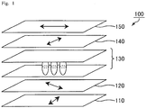
- a CPVA LCD device 100 having the simplest configuration as shown in Fig. 1 , in which a first polarizer 110 (absorption axis azimuth of 90°), a first quarter-wave plate 120 (slow axis azimuth of 135°), a VA LC cell 130, a second quarter-wave plate 140 (slow axis azimuth of 45°), a second polarizer 150 (absorption axis azimuth of 0°), and not including the birefringent layers (II) and (III).
- the arrow shown in each of the first and second polarizers 110 and 150 represents an azimuth of the absorption axis thereof
- the arrow shown in each of the first and second quarter-wave plates 120 and 140 represents an azimuth of the slow axis thereof.
- the ellipsoidal body illustrated in the VA LC cell 130 shows the shape of the refractive index ellipsoidal body of the cell 130.
- a light beam that has entered the first polarizer 110 from the front direction is converted into a linearly-polarized light beam by the first polarizer 110 and then further converted into a circularly-polarized light beam by the first quarter-wave plate 120, and then passes through the LC cell 130 while maintaining its polarization state.
- the circularly-polarized light beam is reconverted into the same linearly-polarized light beam as just at the output of the first polarizer 110, and finally, the linearly-polarized light beam is blocked by the second polarizer 150, which is orthogonal to the first polarizer 110.
- the LCD device 100 can display a perfect black screen in the front direction because (1) the first and second quarter-wave plates 120 and 140 are disposed to be orthogonal to each other between the first and second polarizers 110 and 150, and the retardations thereof are the same ( ⁇ /4) and so the retardation can be canceled.
- the first and second quarter-wave plates are disabled; (2) the LC cell 130 disposed between the first and second polarizers 110 and 150 has a retardation of zero in the front direction, and so it is substantially disabled; and (3) the first and second polarizers 110 and 150 are disposed to be orthogonal to each other, so-called cross-Nicol polarizers.
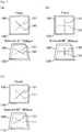
- the slow axis 121 of the first quarter-wave plate 120 and the slow axis 141 of the second quarter-wave plate 140 are orthogonal to each other as schematically shown in Fig. 2(a) , they are not orthogonal to each other in an oblique direction with an azimuth of 0°. Thus the retardation is not cancelled and so the first and second quarter-wave plates 120 and 140 are not disabled. Further, in the front direction, the slow axis 121 of the first quarter-wave plate 120 and the slow axis 141 of the second quarter-wave plate 140 are orthogonal to each other as schematically shown in Fig.
- the CPVA LCD device 100 having the simplest configuration can not display a perfect black screen in the oblique directions because of the three factors (1) to (3). Conversely, elimination of these factors, i.e., optical compensation allows displaying better black screen in the oblique directions.
- the aforementioned technologies (A) to (E) for viewing angle improvement actually involve the optical compensation for the factors.
- the factors (1) and (2) are usually observed together. Accordingly, the optical compensations for the respective factors (1) and (2) may be performed not separately but together.
- the CPVA LCD device of the present invention is so designed to provide optical compensations for the factors (1) to (3) simultaneously based on the following design principle.
- the 1st step means this process where the Nz coefficients Nzq of the first and second quarter-wave plates, the thickness-direction retardation Rlc of the LC cell, and the thickness-direction retardation R3 of the birefringent layer (III) are optimized for optical compensation at an azimuth of 0° as mentioned above.
- the inventor also found that the factors (1), (2), and (3) are simultaneously and effectively eliminated in an oblique direction with an azimuth of 45° by, after the 1st step, disposing the first birefringent layer (II) satisfying the relation of nx ⁇ ny ⁇ nz between the first quarter-wave plate and the first polarizer to have an in-plane fast axis substantially orthogonal to the absorption axis of the first polarizer and disposing the second birefringent layer (II) satisfying the relation of nx ⁇ ny ⁇ nz between the second quarter-wave plate and the second polarizer to have an in-plane fast axis substantially orthogonal to the absorption axis of the second polarizer, and optimizing an Nz coefficient Nz2 and an in-plane retardation R2 of the first and second birefringent layers (II).
- the 2nd step means this process following the 1st step, where the Nz coefficient Nz2 and the in-plane
- the first and second birefringent layers (II), which are additionally disposed in the 2nd step, are disposed such that their in-plane fast axes are substantially orthogonal to the absorption axes of the first and second polarizers, respectively, which are adjacent to the first and second birefringent layers (II), respectively. So the optical characteristics in a direction with an azimuth of 0° are not changed at all.
- the optical compensation of the present invention is characterized in that the optimum state achieved in the 1st step can be maintained even after the 2nd step. This optical compensation way where the 1st and 2nd steps are completely independent from each other simplifies the design of the birefringent layers.
- the Poincare sphere is widely known in crystal optics as a useful approach for tracing polarization state of light propagating through a birefringent layer (for example, see " Kessyo Kogaku", written by Takasaki Hiroshi, published by Morikita Publishing Co., Ltd., 1975, p. 146 to 163 ).
- right-handed polarized state is represented on the upper hemisphere; left-handed polarized state on the lower hemisphere, linear polarized state on the equator; right- and left-handed circular polarized states are on upper and lower poles, respectively.
- the ellipticity angles are the same in magnitude but opposite in polarity. This shows that the two polarization states are in the orthogonal polarization state.
- the effects attributed to the birefringent layer are shown on the Poincare sphere as follows.
- the point showing state of polarization of a light beam before propagating through a birefringent layer is rotated in the counterclockwise direction by an angle determined by (2 ⁇ ) x (retardation)/(wavelength) (unit: rad) around the slow axis (specifically, the point showing the slower of the two eigenmodes of vibration of a birefringent layer) (this is the same when the point is rotated in the clockwise direction around the fast axis).
- the rotation center and the rotation angle in an oblique view direction are determined by the slow axis (or the fast axis) and the retardation at the viewing angle. Although not being explained in detail, these can be calculated, for example, by determining a vibrating direction in the eigenmode of vibration and a wave vector in the birefringent layer from Fresnel equation for the normal incidence.
- the slow axis in oblique view directions depends on a viewing angle and an Nz coefficient.
- the retardation in oblique view directions depends on a viewing angle, an Nz coefficient, and an in-plane retardation R (or a thickness-direction retardation Rth).
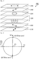
- Fig. 3 is a view showing changes in the polarization state of a light beam emitted from a backlight (not shown in Fig. 1 , but located below the first polarizer) under this condition, represented on S1-S2 plane of the Poincare sphere.
- the points in Fig. 3 show the respective polarization states at the output of the respective polarizers 110 and 150, the respective birefringent layers 120 and 140, and the LC cell 130.
- the points showing the respective polarization states are actually on the Poincare sphere but projected on S1-S2 plane.
- the point showing the polarization state is shown by " ⁇ " and the point showing the slow (fast) axis of the birefringent layer is shown by " ⁇ ".
- the polarization state of the light beam just at the output of the first polarizer 110 is represented by P0 on the Poincare sphere, and P0 corresponds to E showing a polarization state the second polarizer 150 can absorb, i.e., extinction position (absorption axis azimuth) of the second polarizer 150. Then, when the light beam passes through the first quarter-wave plate 120, P0 is moved to P1 by rotation by a specific angle around the slow axis of the first quarter-wave plate 120 represented by Q1 on the Poincare sphere. The rotation is in the counterclockwise direction when the coordinate origin (the center of the Poincare sphere) is viewed from Q1.
- the light beam passes through the VA LC cell 130 but does not change in its polarization state because the cell 130 has a retardation of zero in the front direction.
- the light beam passes through the second quarter-wave plate 140, and P1 is moved to P2 by rotation by a specific angle around the slow axis of the second quarter-wave plate 140 represented by Q2.
- This P2 corresponds to extinction position E of the second polarizer 150.
- the LCD device 100 of Fig. 1 can block the light beam from the backlight to display an excellent black screen when viewed from the front direction.
- Fig. 4 is a view showing changes in the polarization state of a light beam emitted from a backlight under this condition, represented on S1-S2 plane of the Poincare sphere.
- the points in Fig. 4 show the respective polarization states at the output of the respective polarizers 110 and 150, the respective birefringent layers 120 and 140, and the LC cell 130.
- the polarization state of the light beam just at the output of the first polarizer 110 is represented by P0 on the Poincare sphere and P0 corresponds to E showing a polarization state the second polarizer 150 can absorb, i.e., extinction position (absorption axis azimuth) of the second polarizer 150. Then, when the light beam passes through the first quarter-wave plate 120, P0 is moved to P1 by rotation by a specific angle around the slow axis of the first quarter-wave plate 120 represented by Q1 on the Poincare sphere. The rotation is in the counterclockwise direction when the coordinate origin is viewed from Q1.
- the light beam passes through the VA LC cell 130, and P1 reaches P2 by rotation by a specific angle around the slow axis of the LC cell 130 represented by L on the Poincare sphere.
- the rotation is in the counterclockwise direction when the coordinate origin is viewed from L.
- the light beam passes through the second quarter-wave plate 140, and P2 is moved to P3 by rotation by a specific angle around the slow axis of the second quarter-wave plate 140 represented by Q2.
- This P3 does not correspond to extinction position E of the second polarizer 150.
- the LCD device 100 of Fig. 1 can not block the light beam from the backlight when viewed from the direction with an azimuth of 0° and a polar angle of 60°.
- the positions of P1 to P3 in Figs. 3 and 4 depend on the Nz coefficients Nzq of the first and second quarter-wave plates 120 and 140 and the thickness-direction retardation Rlc of the LC cell 130.
- the retardation Rlc of the VA LC cell 130 is typically about 320 nm, and usually adjusted to a value ranging from 270 nm to 400 nm.
- the retardation Rlc is required to be larger than 320 nm in order to increase the transmittance.
- the Nz coefficient Nzq of each of the first and second quarter-wave plates 120 and 140 is usually adjusted to a value ranging from 1.0 to 2.9.
- a CPVA LCD device 200 including the birefringent layer (III) as shown in Fig. 5 , in which a first polarizer 210 (absorption axis azimuth of 90°), a first quarter-wave plate 220 (slow axis azimuth of 135°), a VA LC cell 230, a birefringent layer (III) 235, a second quarter-wave plate 240 (slow axis azimuth of 45°), and a second polarizer 250 (absorption axis azimuth of 0°) are stacked in this order.
- a first polarizer 210 absorption axis azimuth of 90°
- a first quarter-wave plate 220 low axis azimuth of 135°
- VA LC cell 230 a birefringent layer (III) 235
- a second quarter-wave plate 240 slow axis azimuth of 45°
- a second polarizer 250 (absorption axis azimuth
- the arrow shown in each of the first and second polarizers 210 and 250 represents an azimuth of the absorption axis thereof
- the arrow shown in each of the first and second quarter-wave plates 220 and 240 represents an azimuth of the slow axis thereof.
- the ellipsoidal bodies in the VA LC cell 230 and the birefringent layer (III) 235 show the shape of the respective refractive index ellipsoidal bodies thereof.
- Fig. 6 is a view showing changes in the polarization state of a light beam emitted from a backlight (not shown in Fig. 5 , but located below the first polarizer 210) under this condition, represented on S1-S2 plane of the Poincare sphere.
- the points in Fig. 6 show the respective polarization states at the output of the respective polarizers 210 and 250, the respective birefringent layers 220 and 240, and the LC cell 230.
- the polarization state of the light beam just at the output of the first polarizer 210 is represented by P0 on the Poincare sphere, and P0 corresponds to E showing a polarization state the second polarizer 250 can absorb, i.e., extinction position (absorption axis azimuth) of the second polarizer 250. Then, when the light beam passes through the first quarter-wave plate 220, P0 is moved to P1 by rotation by a specific angle around the slow axis of the first quarter-wave plate 220 represented by Q1 on the Poincare sphere. The rotation is in the counterclockwise direction when the coordinate origin is viewed from Q1.
- the light beam passes through the VA LC cell 230 and the birefringent layer (III) 235 but does not change in its polarization state because the cell 230 and the birefringent layer (III) 235 each have a retardation of zero in the front direction.
- the light beam passes through the second quarter-wave plate 240, and P1 is moved to P2 by rotation by a specific angle around the slow axis of the second quarter-wave plate 240 represented by Q2. This P2 corresponds to extinction position E of the second polarizer 250.
- the LCD device 200 of Fig. 5 can block the light beam from the backlight to display an excellent black screen when viewed from the front direction, as in the LCD device 100 in Fig. 1 .
- Fig. 7 is a view showing changes in the polarization state of a light beam emitted from a backlight under this condition, represented on S1-S2 plane of the Poincare sphere.
- the points in Fig. 7 show the respective polarization states at the output of the respective polarizers 210 and 250, the respective birefringent layers 220 and 240, and the LC cell 230.
- the polarization state of the light beam just at the output of the first polarizer 210 is represented by P0 on the Poincare sphere and P0 corresponds to E showing a polarization state the second polarizer 250 can absorb, i.e., extinction position (absorption axis azimuth) of the second polarizer 250. Then, when the light beam passes through the first quarter-wave plate 220, P0 reaches P1 by rotation by a specific angle around the slow axis of the first quarter-wave plate 220 represented by Q1 on the Poincare sphere. The rotation is in the counterclockwise direction when the coordinate origin is viewed from Q1.
- the light beam passes through the VA LC cell 230, and P1 reaches P2 by rotation by a specific angle around the slow axis of the LC cell 230 represented by L on the Poincare sphere.
- the rotation is in the counterclockwise direction when the coordinate origin is viewed from L.
- the light beam passes through the birefringent layer (III) 235, and P2 reaches P3 by rotation by a specific angle around the slow axis of the birefringent layer (III) 235, represented by R3 on the Poincare sphere.
- the rotation is in the counterclockwise direction when the coordinate origin is viewed from R3.
- the LCD device 200 of Fig. 5 can block the light beam from the backlight when viewed from the direction with an azimuth of 0° and a polar angle of 60°, as in viewing from the front direction.
- Figs. 8 and 9 are views each showing changes in the polarization state when the CPVA LCD device 200 in Fig. 5 is viewed from the direction with an absorption axis azimuth 0° of the second polarizer 250 and a polar angle of 60°, represented on S1-S2 plane of the Poincare sphere.
- the retardation Rlc of the VA LC cell 230 is adjusted to a value ranging from 270 nm to 400 nm, and so when the Nz coefficient Nzq of each of the first and second quarter-wave plates 220 and 240 is 2.00 or smaller, there is a great need to dispose the birefringent layer (III) .
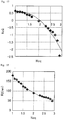
- Table 2 and Fig. 10 show a relationship between the Nz coefficient Nzq of each of the first and second quarter-wave plates 220 and 240 and the optimum thickness-direction retardation R3 of the birefringent layer (III) 235, based on the results determined by computer simulations.
- the polarization conversion from P1 to P3 is illustrated separately into P1 to P2 conversion attributed to the thickness-direction retardation Rlc of the VA LC cell 230 and into P2 to P3 conversion attributed to the thickness-direction retardation R3 of the birefringent layer (III) 235.
- these two conversions are the same in rotation center, just opposite in rotation direction.
- the rotation direction is determined by a plus and minus sign of the thickness-direction retardation.
- the rotation angle is determined by the magnitude of the thickness-direction retardation. Accordingly, the above-mentioned two conversions can be regarded as a direct conversion P1 to P3 attributed to "the total thickness-direction retardation Rlc + R3" of the "VA LC cell 230 + the birefringent layer (III) 235". In other words, regardless of the thickness-direction retardation Rlc of the VA LC cell 230, the optical characteristics are the same among the LCD devices whose Rlc+ R3 are the same. Table 2 shows the optimum values Rlc + R3 calculated by computer simulations. As shown in Table 2 and Fig.
- the retardation Rlc + R3 which is the sum of the thickness-direction retardation Rlc in a black state (in the absence of an applied voltage to the LC layer) of the VA LC cell 230 and the thickness-direction retardation R3 of the birefringent layer (III) 235 is most preferably the optimum value shown in Table 2 and Fig. 10 .
- the value may slightly deviate from the optimum value unless the contrast ratio in oblique directions is significantly reduced.
- it is preferable that the retardation Rlc + R3 is within the optimum value ⁇ 30 nm.
- the LCD device 200 of Fig. 5 after the 1st step is viewed from a direction with an azimuth (hereinafter, also referred to as an "azimuth of 45°") bisecting the absorption axis azimuth of 90° of the first polarizer 210 and the absorption axis azimuth of 0° of the second polarizer 250 and the direction inclined by 60°.
- azimuth hereinafter, also referred to as an "azimuth of 45°
- the LCD device 200 achieves the optical compensation at an azimuth of 0° by determining the optimum values each of the thickness-direction retardation Rlc of the LC cell 230 and the thickness-direction retardation R3 of the birefringent layer (III) 235 in accordance with the Nz coefficient Nzq of each of the first and second ⁇ /4 retarders 220 and 240.
- Fig. 11 is a view showing changes in the polarization state of a light beam emitted from a backlight under this condition, represented on S1-S2 plane of the Poincare sphere. The points in Fig. 11 show the respective polarization states at the output of the respective polarizers 210 and 250, the respective birefringent layers 220 and 240, and the LC cell 230.
- the polarization state of the light beam just at the output of the first polarizer 210 is represented by P0 on the Poincare sphere, and P0 does not correspond to E showing a polarization state the second polarizer 250 can absorb, i.e., extinction position (absorption axis azimuth) of the second polarizer 250.
- P0 does not correspond to E showing a polarization state the second polarizer 250 can absorb, i.e., extinction position (absorption axis azimuth) of the second polarizer 250.
- P0 is moved to P1 by rotation by a specific angle around the slow axis of the first quarter-wave plate 220 represented by Q1 on the Poincare sphere.
- the rotation is in the counterclockwise direction when the coordinate origin is viewed from Q1.
- the light beam passes through the VA LC cell 230, and P1 is moved to P2 by rotation by a specific angle around the slow axis of the LC cell 230 represented by L on the Poincare sphere.
- This rotation is in the counterclockwise direction when the coordinate origin is viewed from L.
- the light beam passes through the birefringent layer (III) 235, and P2 reaches P3 by rotation by a specific angle around the slow axis of the birefringent layer (III) 235 represented by R3 on the Poincare sphere.
- the rotation is in the counterclockwise direction when the coordinate origin is viewed from R3.
- the LCD device 200 of Fig. 5 can not block the light beam from the backlight when viewed from the oblique direction with an azimuth of 45° and a polar angle of 60°. Specifically, the optical compensation is not achieved when the LCD device 200 just having undergone the 1st step is viewed from the oblique direction with an azimuth of 45°.
- the positions of P1 to P4 in Fig. 11 depend on the Nz coefficient Nzq of each of the first and second quarter-wave plates 220 and 240, the thickness-direction retardation Rlc of the LC cell 230, and the thickness-direction retardation R3 of the birefringent layer (III) 235.
- the positions of the respective points are roughly shown and might not be strictly accurate.
- the arrows showing the locus of P1-P4 conversion are not shown.
- a CPVA LCD device 300 including birefringent layers (II) as shown in Fig. 12 , in which a first polarizer 310 (absorption axis azimuth of 90°), a first birefringent layer (II) 315 (fast axis azimuth of 0°), a first quarter-wave plate 320 (slow axis azimuth of 135°), a VA LC cell 330, a birefringent layer (III) 335, a second quarter-wave plate 340 (slow axis azimuth of 45°), a second birefringent layer (II) 345 (fast axis azimuth of 90°), and a second polarizer 350 (absorption axis azimuth of 0°) are stacked in this order.
- a first polarizer 310 absorption axis azimuth of 90°
- a first birefringent layer (II) 315 fast axis azimuth of 0°
- the first and second birefringent layers (II) are added for optical compensation at an azimuth of 45°.
- the arrow shown in each of the first and second polarizers 310 and 350 represents an azimuth of the absorption axis thereof; the arrow shown in each of the first and second quarter-wave plates 320 and 340 represents an azimuth of the slow axis thereof; and the arrow shown in the first and second birefringent layers (II) 315 and 345 represents an azimuth of the fast axis thereof.
- the ellipsoidal bodies in the VA LC cell 330 and the birefringent layer (III) 335 show the shape of the respective refractive index ellipsoidal bodies thereof.
- Fig. 13 is a view showing changes in the polarization state of a light beam emitted from a backlight (not shown in Fig. 12 , but located below the first polarizer 310), represented on S1-S2 plane of the Poincare sphere.
- the points in Fig. 13 show the respective polarization states at the output of the respective polarizers 310 and 350, the respective birefringent layers 315, 320, 340, and 345, and the LC cell 330.
- the polarization state of the light beam just at the output of the first polarizer 310 is represented by P0 on the Poincare sphere, and P0 corresponds to E showing a polarization state the second polarizer 350 can absorb, i.e., extinction position (absorption axis azimuth) of the second polarizer 350.
- the light beam passes through the first birefringent layer (II) 315, but the polarization state thereof represented by P0 is not changed even after the rotation by a specific angle around the fast axis of the first birefringent layer (II) 315 represented by R2-1 on the Poincare sphere.
- the light beam passes through the VA LC cell 330 and the birefringent layer (III) 335 but does not change in its polarization state because the cell 330 and the birefringent layer (III) 335 each have a retardation of zero in the front direction.
- the light beam passes through the second quarter-wave plate 340, and P1 is moved to P2 by rotation by a specific angle around the slow axis of the second quarter-wave plate 340 represented by Q2.
- the light beam passes through the second birefringent layer (II) 345, but the polarization state thereof represented by P2 is not changed even after the rotation by a specific angle around the fast axis of the second birefringent layer (II) 345 represented by R2-2 on the Poincare sphere.
- This P2 corresponds to extinction position E of the second polarizer 350.
- the LCD device 300 of Fig. 12 can block the light beam from the backlight to display an excellent black screen when viewed from the front direction, as in the LCD device 100 of Fig. 1 .
- Fig. 14 is a view showing changes in the polarization state of a light beam emitted from a backlight under this condition, represented on S1-S2 plane of the Poincare sphere.
- the points in Fig. 14 show the respective polarization states at the output of the respective polarizers 310 and 350, the respective birefringent layers 315, 320, 340, and 345, and the LC cell 330.
- the polarization state just at the output of the first polarizer 310 is represented by P0 on the Poincare sphere, and P0 does not correspond to E showing a polarization state the second polarizer 350 can absorb, i.e., extinction position (absorption axis azimuth) of the second polarizer 350.
- P0 is moved to P1 by rotation by a specific angle around the fast axis of the first birefringent layer (II) 315 represented by R2-1 on the Poincare sphere.
- the light beam passes through the VA LC cell 330, and P2 is moved to P3 by rotation by a specific angle around the slow axis of the LC cell 330 represented by L on the Poincare sphere.
- This rotation is in the counterclockwise direction when the coordinate origin is viewed from L.
- the light beam passes through the birefringent layer (III) 335, and P3 reaches P4 by rotation by a specific angle around the slow axis of the birefringent layer (III) 335 represented by R3 on the Poincare sphere.
- the rotation is in the counterclockwise direction when the coordinate origin is viewed from R3.
- the light beam passes through the second quarter-wave plate 340, and P4 reaches P5 by rotation by a specific angle around the slow axis of the second quarter-wave plate 340 represented by Q2.
- the light beam passes through the second birefringent layer (II) 345, and P5 is moved to P6 by rotation by a specific angle around the fast axis of the second birefringent layer (II) 345 represented by R2-2 on the Poincare sphere.
- the rotation is in the clockwise direction when the coordinate origin is viewed from R2-2.
- This P6 corresponds to extinction position E of the second polarizer 350.
- the LCD device 300 of Fig. 12 can block the light beam from the backlight when viewed from the oblique direction with an azimuth of 45° and a polar angle of 60°, similarly in the front direction.
- Fig. 15 is a view showing changes in the polarization state of a light beam emitted from a backlight under this condition, represented on S1-S2 plane of the Poincare sphere.
- the points in Fig. 15 show the respective polarization states at the output of the respective polarizers 310 and 350, the respective birefringent layers 315, 320, 340, and 345, and the LC cell 330.
- the polarization state of the light beam just at the output of the first polarizer 310 is represented by P0 on the Poincare sphere and P0 corresponds to E showing a polarization state the second polarizer 350 can absorb, i.e., extinction position (absorption axis azimuth) of the second polarizer 350.
- the light beam passes through the first birefringent layer (II) 315, but the polarization state thereof represented by P0 is not changed even after the rotation by a specific angle around the fast axis of the first birefringent (II) 315 represented by R2-1 on the Poincare sphere.
- the light beam passes through the VA LC cell 330, and P1 reaches P2 by rotation by a specific angle around the slow axis of the LC cell 330, represented by L on the Poincare sphere.
- the rotation is in the counterclockwise direction when the coordinate origin is viewed from L.
- the light beam passes through the birefringent layer (III) 335, and P2 reaches P3 by rotation by a specific angle around the slow axis of the birefringent layer (III) 335, represented by R3 on the Poincare sphere.
- the rotation is in the counterclockwise direction when the coordinate origin is viewed from R3.
- the LCD device 300 of Fig. 12 can block the light beam from the backlight to display an excellent black screen when viewed from the oblique direction with an azimuth of 0° and a polar angle of 60°, similarly in the front direction.
- the LCD device 300 in Fig. 12 having undergone the 2nd step can block the light beam from the backlight to display an excellent black screen in each of the front direction, the oblique direction with an azimuth of 0°, and the oblique direction with an azimuth of 45°.
- the positions of P1 to P6 in Figs. 13, 14 , and 15 depend on the Nz coefficient Nzq of each of the first and second quarter-wave plates 320 and 340, the thickness-direction retardation Rlc of the LC cell 330, the thickness-direction retardation R3 of the birefringent layer (III) 335, and the Nz coefficient Nz2 and the in-plane retardation R2 of each of the first and second birefringent layers (II) 315 and 345.
- Fig. 16 is a view showing changes in the polarization state when the CPVA LCD device 300 in Fig. 12 is viewed from the oblique direction with an absorption axis azimuth 45° of the second polarizer 350 and a polar angle of 60°, represented on S1-S2 plane of the Poincare sphere.
- Table 3 and Figs. 17 and 18 show a relationship between the Nz coefficients Nzq of the first and second quarter-wave plates 320 and 340, and the optimum values of the Nz coefficient Nz2 and the in-plane retardation R2 of each of the first and second birefringent layers (II) 315 and 345, based on the results determined by computer simulations.
- the relationship between Nzq, and the optimum Nz2 and R2 is not simple typically, but in the case of 1.0 ⁇ Nzq ⁇ 2.9, the following (B) and (C) give a sufficiently close approximation to Nz2 and R2, respectively, which are shown by solid lines in Figs. 17 and 18 .
- Nz 2 ⁇ 0.87 ⁇ Nzq 2 + 2.15 ⁇ Nzq ⁇ 0.76
- R 2 25 nm ⁇ Nzq 2 ⁇ 159 nm ⁇ Nzq + 311 nm
- the values Nz2 and R2 of the first and second birefringent layers (II) 315 and 345 are most preferably the optimum values shown in Table 3 and Figs. 17 and 18 , respectively, in order to provide LC display with a high contrast ratio in a wide viewing angle range. However, the values may slightly deviate from the respective optimum values unless the contrast ratio in oblique directions is significantly reduced.
- the Nz coefficient Nz2 is preferably within the optimum value ⁇ 0.45.
- the in-plane retardation R2 is preferably within the optimum value ⁇ 40 nm.
- the optimum value Nz2 is in a range of 0 ⁇ Nz2 ⁇ 1.
- the birefringent layer having the Nz coefficient satisfying this range is a biaxial retardation film satisfying nx > nz > ny. Accordingly, such a layer does not correspond to the birefringent layer (II) and is an expensive film that is harder to produce than the birefringent layer (II) is.
- the present inventor made various investigations on a simple and cost-effective method of providing LC display with a high contrast ratio in a wide viewing angle range in the case of Nzq ⁇ 2.00.
- Nzq Nz2 R2' (nm) R2' (nm) 1.0 0.65 180 45 1.1 0.60 162 53 1.2 0.60 158 60 1.3 0.55 147 65 1.4 0.50 138 71 1.5 0.40 123 75 1.6 0.35 118 80 1.7 0.25 108 84 2.0 -0.05 89 93 2.3 -0.40 77 2.4 -0.55 73 2.5 -0.70 69 2.6 -0.80 68 2.7 -1.00 64 2.8 -140 59 2.9 -2.45 49
- the LCD device of the present invention can be easily produced and has a high contrast ratio in a wide viewing angle range.
- Such an LCD device of the present invention can be preferably used in display devices such as outdoor signage displays.
- materials and optical characteristics thereof are not especially limited.
- the materials include thin plates made of inorganic materials, stretched polymer films, and ones in which alignment of liquid crystalline molecules is fixed.
- the method for forming the birefringent layers is not especially limited.
- the polymer films may be formed by solvent cast, melt extrusion, and the like. Alternatively, coextrusion may be employed to form a plurality of birefringent layers at a time.
- the polymer films may or may not be stretched as long as desired retardations can be exhibited.
- the stretching method is not especially limited.
- the polymer films may be stretched under tension between rolls, compressed and stretched between rolls, uniaxially stretched in a transverse direction with a tenter, stretched in an oblique direction, or biaxially stretched in longitudinal and transverse directions.
- the polymer films may be stretched under the influence of contractile force of a thermo-shrinkable film.
- the oblique stretching is preferably employed in which a material for the quarter-wave plate is stretched in a direction oblique to a feeding direction of a roll film because the quarter-wave plate is stacked on a polarizer so as to form a relative angle of about 45° with the polarizer to serve as a circular polarizer.
- the liquid crystalline material is applied on a base film with an alignment treatment-provided surface, and thereby fixing alignment of the liquid crystalline material.
- the base film may not be provided with the alignment treatment or the coating may be separated from the base film after the alignment fixing to be transferred onto another film as long as the desired retardations are exhibited.
- the alignment of the LC materials may not be fixed.
- the same methods as in use of the liquid crystalline materials may be employed when non-crystalline materials are used to form the birefringent layers. The following will in more detail describe the birefringent layers classified by types.
- the birefringent layer (I) for example, materials formed by stretching a film containing a component with positive intrinsic birefringence may be appropriately used.
- the component with positive intrinsic birefringence include polycarbonate, polysulfone, polyether sulfone, polyethylene terephthalate, polyethylene, polyvinyl alcohol, norbornene, triacetyl cellulose, and diatyl cellulose.
- the birefringent layer (II) may include, for example, a material formed by stretching a film containing a component with negative intrinsic birefringence and one formed by stretching a film containing a component with positive intrinsic birefringence under the influence of contractile force of a thermo-shrinkable film.
- a material formed by stretching a film containing a component with negative intrinsic birefringence and one formed by stretching a film containing a component with positive intrinsic birefringence under the influence of contractile force of a thermo-shrinkable film.
- one formed by stretching a film containing a component with negative intrinsic birefringence is preferable.
- the component with negative intrinsic birefringence examples include resin compositions containing an acrylic resin and a styrene resin, polystyrene, polyvinyl naphthalene, polyvinyl biphenyl, polyvinyl pyridine, polymethyl methacrylate, polymethyl acrylate, an N-substituted maleimide copolymer, fluorene skeleton-containing polycarbonate, and triacetyl cellulose (particularly with a small acetylation degree).
- resin compositions containing an acrylic resin and a styrene resin are particularly preferable as the component with negative intrinsic birefringence.
- Japanese Kokai Publication No. 2008-146003 discloses a production method of a film containing such a resin composition.
- the birefringent layer (III) may include a material formed by stretching in longitudinal and transverse directions a film containing a component with positive intrinsic birefringence, one coated with a liquid crystalline compound e.g. a cholesteric (chiral nematic) liquid crystal and a discotic liquid crystal, and one coated with a non-liquid crystalline compound including polyimide, polyamide, and the like.
- a liquid crystalline compound e.g. a cholesteric (chiral nematic) liquid crystal and a discotic liquid crystal
- a non-liquid crystalline compound including polyimide, polyamide, and the like.
- the polarizers may include a polyvinyl alcohol (PVA) film with a dichroic anisotropic material such as an iodine complex adsorbed and aligned thereon.
- PVA polyvinyl alcohol
- the LC cell is not especially limited as long as it can display a black screen by aligning LC molecules in the LC cell vertically to the substrate surface, and VA LC cells may be employed, for example.
- VA LC cells include MVA, CPA, PVA, BVA, RTN, and IPS-VA cells.
- Examples of a driving system of the LC cell include TFT system (active matrix system), passive matrix system, and plasma address system.
- the LC cell has a configuration, for example, in which an LC layer is disposed between a pair of substrates each provided with electrodes and display is provided by voltage application between the electrodes.
- R, Rth, Nz coefficient, nx, ny, and nz were measured with a dual-rotating retarder polarimeter (Axo-scan, Axometrics, Inc.).
- In-plane retardation R was measured from the normal direction of the birefringent layer.
- Principal refractive indices nx, ny, and nz, thickness-direction retardation Rth, and Nz coefficient were calculated by curve fitting with a known index ellipsoid. For the calculation, retardations of the birefringent layer were measured from the normal direction and the directions each with a polar angle of -50° to 50° from the normal direction.
- the average refractive index of each birefringent layer was set to 1.5. Even in the case of the birefringent layer having an actual average refractive index of not 1.5, the average refractive index was converted into 1.5.
- the viewing angle dependence of contrast was measured with a viewing angle measuring apparatus (EZContrast 160, ELDIM).
- the light source was a backlight mounted on a LC TV (LC37-GH1, SHARP Corp.).
- Brightnesses upon displaying a white screen and a black screen were measured in the oblique direction with an azimuth of 45° and a polar angle of 60°. The ratio thereof was regarded as CR (45, 60).
- Brightnesses upon displaying a white screen and a black screen were measured in the oblique direction with an azimuth of 0° and a polar angle of 60°. The ratio thereof was regarded as CR (0, 60).
- the LCD devices in embodiments 1 to 4 of the present invention are a CPVA LCD device 300 in which as shown in Fig. 12 , a first polarizer 310, a first birefringent layer (II) 315, a first quarter-wave plate (birefringent layer (I)) 320, a VA LC cell 330, a birefringent layer (III) 335, a second quarter-wave plate 340, a second birefringent layer (II) 345, and a second polarizer 350 are stacked in this order.
- a first polarizer 310 a first birefringent layer (II) 315, a first quarter-wave plate (birefringent layer (I)) 320, a VA LC cell 330, a birefringent layer (III) 335, a second quarter-wave plate 340, a second birefringent layer (II) 345, and a second polarizer 350 are stacked in this order.
- the arrow in each of the first and second polarizers 310 and 350 shows an azimuth of the absorption axis thereof; the arrow in each of the first and second quarter-wave plates 320 and 340 shows an azimuth of the slow axis thereof; the arrow in each of the first and second birefringent layer (II) 315 and 345 shows an azimuth of the fast axis thereof; and the ellipsoidal body in the VA LC cell 330 and the birefringent layer (III) 335 shows the shape of the refractive index ellipsoidal body thereof.
- the LCD device of comparative embodiment 1 is a VA LCD device in which a first polarizer, a TAC film, a first quarter-wave plate (birefringent layer (I)), a VA LC cell, a second quarter-wave plate, a TAC film, and a second polarizer are stacked in this order.
- the LCD device of comparative embodiment 2 is a VA LCD device in which a first polarizer, a TAC film, a first quarter-wave plate (birefringent layer (I)), a VA LC cell, a birefringent layer (III), a second quarter-wave plate, a TAC film, and a second polarizer are stacked in this order.
- the material name, axis angle, in-plane retardation R, thickness-direction retardation Rth or Rlc, and Nz coefficient of the polarizers, the birefringent layers, and the LC cell of the respective embodiments are as shown in the following Table 4 (embodiments 1 to 4) and Table 5 (comparative embodiments 1 and 2).
- the axis of each of the birefringent layers is defined by an azimuth angle of the in-plane slow axis
- the axis of each of the polarizers is defined by an azimuth angle of the absorption axis.
- the design of the in-plane fast axis is important, and in Tables, the axis of the birefringent layer (II) is defined by an azimuth angle of the in-plane slow axis, as in other birefringent layers.
- the in-plane fast axis of the birefringent layer (II) is orthogonal to the in-plane slow axis of the birefringent layer (II).
- the name of the materials of the respective birefringent layers is indicated by means of the following abbreviations.
- the viewing angle dependence of contrast ratio of the LCD device was determined in each embodiment, and the CR (0, 60) and the CR (45, 60) are shown in Tables 4 and 5.
- the LCD device in each of embodiments 1 to 4 according to the present invention had a CR (0, 60) and a CR (45, 60) that are much higher than those in the LCD device in each of comparative embodiments 1 and 2. Even in the visual evaluation, the LCD devices of embodiments 1 to 4 each had a contrast ratio on the viewing angle that is much superior to that in the LCD devices of comparative embodiments 1 and 2.
- Second polarizer -20 5 40 TAC TAC 1 32 Second quarter-wave plate NB 25 138 1.
- the LCD device in each of embodiments includes a circularly-polarizing plate composed of a linearly-polarizing plate (second polarizer) and a quarter-wave plate on each side of the LC cell to provide display in CPVA mode.
- the CPVA mode is effective in improvement of contrast ratio because the anti-reflection effects can be obtained in addition to the transmittance-improvement effects.
- the circularly-polarizing plates inhibit a light beam once having entered the LCD device and then being reflected inside the device, i.e., a reflected light beam by internal reflection, from exiting the LCD device. Accordingly, in the CPVA mode, light beams reflected on black matrix, the lines, the electrodes, and the like in the LC cell hardly exit the LCD devices, and particularly in bright environments, the reduction in contrast ratio of the LCD devices can be prevented.
- Examples of the reflected light beams causing a reduction in contrast ratio of the LCD devices in bright environments include a light beam that has been reflected on the surface of the LCD device without entering the device, i.e., a reflected light beam by surface reflection, in addition to the reflected light by internal reflection.
- the CPVA LCD device the amount of the reflected light beam by the surface reflection has large effects on visibility of the display screen because the reflected light beam by internal reflection is suppressed. Accordingly, by providing the CPVA LCD device with a measure for reducing the light reflected by the surface reflection, the device can provide a very high contrast ratio in bright environments, and a viewer can realize a marked improvement in display qualities.
- the anti-reflection film for suppression of the surface reflection includes one having a multi-layer structure composed of films with different refractive indices, and one having a surface on which fine protrusions and recesses are formed.
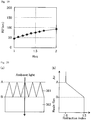
- a "moth-eye film” which is one kind of the latter one, has a surface on which many protrusions smaller than a wavelength (380 nm to 780 nm) of a visible light beam are formed, and due to this structure, very excellent effects of suppressing the surface reflection can be exhibited. As shown in Fig.
- a light beam entering the moth-eye film reaches a base material portion 362 through fine protrusions 361 formed on the surface, and so a region where both of the protrusions and air exist between air and the base material portion (A-B region in Fig. 20(a) ) is regarded as a region with a refractive index intermediate between that of a material constituting the film (about 1.5 if a resin constitutes the film) and that of air (1.0).
- a region with a refractive index intermediate between that of a material constituting the film about 1.5 if a resin constitutes the film
- the refractive index in this region continuously and gradually increases with a change in volume ratio between the protrusion and air, within the distance shorter than the wavelength of the visible light beam from the refractive index of air in contact with the film surface to the refractive index of the material for the film.
- a light beam incident on the moth-eye film does not recognize the air-film interface as an interface of the two with different refractive indices, and reflection of the light beam on the interface can be significantly reduced.
- a surface reflectance of a visible light beam can be reduced to about 0.15%.
- the moth-eye films are disposed between two media with different refractive indices to reduce a reflectance of a light beam on the interface therebetween, but in the configuration in Fig. 12 , the internal reflection occurring on the inner side of the second polarizer 350 can be suppressed by the circularly-polarizing plate composed of the second polarizer 350 and the second quarter-wave plate 340. Accordingly, when the configuration in Fig. 12 .is provided with a moth-eye film, the film is disposed on the display face side of the second polarizer 350, like a moth-eye film 360 shown in Fig. 21 .
- a moth-eye film may be disposed at each interface and preferably disposed at least on the surface of the LCD device that is exposed to the outside.
- the moth-eye film include a resin film having a surface on which many protrusions each having a substantially conical shape with a height of about 200 nm are formed with a distance between the tops of the cones being about 200 nm.
- Nanoimprint technology may be employed for production of the moth-eye film.
- employed may be a technology of transferring protrusions and recesses in nanometer size (1 to 1000 ⁇ m) of a mold surface to a resin material coated over a substrate.
- thermal nanoimprint, UV nanoimprint, and the like may be employed.
- UV nanoimprint for example, a mold is pressed against a UV-curable resin film formed on a transparent substrate, and the film is irradiated with UV light, thereby producing a thin film with moth-eye structure in the inverse shape of the mold on the transparent substrate.
- Roll-to-roll process is better than batch process when nanoimprint technology is used to produce a large number of thin films with a moth-eye structure at a low cost.
- a mold roller includes one having nanosized recesses formed on a polished outer circumference surface of a conical or cylindrical aluminum tube by anodization. According to anodization, the nanosized recesses can be formed in a random placement and in an almost uniform distribution, and seamless moth-eye structures preferable for continuous production can be formed on a mold roller surface.
Landscapes
- Physics & Mathematics (AREA)
- General Physics & Mathematics (AREA)
- Optics & Photonics (AREA)
- Chemical & Material Sciences (AREA)
- Crystallography & Structural Chemistry (AREA)
- Nonlinear Science (AREA)
- Mathematical Physics (AREA)
- Polarising Elements (AREA)
- Liquid Crystal (AREA)
Claims (3)
- Flüssigkristallanzeigevorrichtung (300), in der folgenden Reihenfolge aufweisend:einen ersten Polarisator (310);eine erste doppelbrechende Schicht II (315);eine erste doppelbrechende Schicht I (320) mit einer auf λ/4 eingestellten Verzögerung in einer Ebene;eine Flüssigkristallzelle (330), die ein Paar einander gegenüberliegende Substrate und eine dazwischen angeordnete Flüssigkristallschicht umfasst;eine zweite doppelbrechende Schicht I (340) mit einem Nz-Koeffizienten, der im Wesentlichen gleich demjenigen der ersten doppelbrechenden Schicht I (320) ist, und einer auf λ/4 eingestellten Verzögerung in einer Ebene;eine zweite doppelbrechende Schicht II (345) mit einem Nz-Koeffizienten und einer Verzögerung in einer Ebene, die im Wesentlichen gleich einem Nz-Koeffizienten bzw. einer Verzögerung in einer Ebene der ersten doppelbrechenden Schicht II (315) sind; undeinen zweiten Polarisator (350), unter der Voraussetzung, dass die doppelbrechenden Schichten I (320, 340) als eine doppelbrechende Schicht definiert sind, die die Beziehung nx > ny ≥ nz erfüllt; die doppelbrechenden Schichten II (315, 345) als eine doppelbrechende Schicht definiert sind, die die Beziehung nx < ny ≤ nz erfüllt; und eine doppelbrechende Schicht III (335) als eine doppelbrechende Schicht definiert ist, die die Beziehung nx ≈ ny ≥ nz erfüllt,wobeidie Vorrichtung zumindest eine doppelbrechende Schicht III (335) aufweist, die zwischen der ersten doppelbrechenden Schicht I (320) und der Flüssigkristallzelle (330) und/oder zwischen der Flüssigkristallzelle (330) und der zweiten doppelbrechenden Schicht I (340) angeordnet ist,die erste doppelbrechende Schicht I (320) eine langsame Achse in einer Ebene aufweist, die einen Winkel von etwa 45° mit einer Absorptionsachse des ersten Polarisators (310) bildet,die zweite doppelbrechende Schicht I (340) eine langsame Achse in einer Ebene aufweist, die zur langsamen Achse in einer Ebene der ersten doppelbrechenden Schicht I (320) im Wesentlichen orthogonal ist,der zweite Polarisator (350) eine Absorptionsachse aufweist, die zur Absorptionsachse des ersten Polarisators (310) im Wesentlichen orthogonal ist,die erste doppelbrechende Schicht II (315) eine schnelle Achse in einer Ebene aufweist, die zur Absorptionsachse des ersten Polarisators (310) im Wesentlichen orthogonal ist;die zweite doppelbrechende Schicht II (345) eine schnelle Achse in einer Ebene aufweist, die zur Absorptionsachse des zweiten Polarisators (350) im Wesentlichen orthogonal ist, unddie Vorrichtung einen schwarzen Schirm anzeigt, indem Flüssigkristallmoleküle in der Flüssigkristallschicht im Wesentlichen vertikal zur Substratoberfläche ausgerichtet werden; und gekennzeichnet dadurch, dassdie Flüssigkristallanzeigevorrichtung Nzq < 2,00, -0,45 ≤ Nz2 ≤ 0 und 5 nm ≤ R2 ≤ 133 nm erfüllt, wobei der Nz-Koeffizient jeder der ersten und zweiten doppelbrechenden Schichten I (320, 340) als Nzq definiert ist; der Nz-Koeffizient jeder der ersten und zweiten doppelbrechenden Schichten II (315, 345) als Nz2 definiert ist; und die Verzögerung in einer Ebene jeder der ersten und zweiten doppelbrechenden Schichten II (315, 345) als R2 definiert ist.
- Flüssigkristallanzeigevorrichtung nach Anspruch 1,
wobei die Flüssigkristallanzeigevorrichtung die folgenden Formeln [1] bis [3] erfüllt:


eine Verzögerung in Dickenrichtung der Flüssigkristallzelle (330) in einem Zustand des schwarzen Schirms als Rlc definiert ist;
die Summe von Verzögerungen in Dickenrichtungen der zumindest einen doppelbrechenden Schicht III (335), die zwischen der ersten doppelbrechenden Schicht I (320) und der zweiten doppelbrechenden Schicht I (340) angeordnet ist, als R3 definiert ist. - Flüssigkristallanzeigevorrichtung nach Anspruch 1,
wobei die Flüssigkristallanzeigevorrichtung ferner einen Antireflexionsfilm aufweist, der eine Oberfläche hat, auf der Erhebungen (361), die kleiner als eine Wellenlänge sichtbaren Lichts sind, ausgebildet sind.
Applications Claiming Priority (2)
| Application Number | Priority Date | Filing Date | Title |
|---|---|---|---|
| JP2009127933 | 2009-05-27 | ||
| PCT/JP2010/053351 WO2010137372A1 (ja) | 2009-05-27 | 2010-03-02 | 液晶表示装置 |
Publications (3)
| Publication Number | Publication Date |
|---|---|
| EP2437106A1 EP2437106A1 (de) | 2012-04-04 |
| EP2437106A4 EP2437106A4 (de) | 2017-04-05 |
| EP2437106B1 true EP2437106B1 (de) | 2020-11-18 |
Family
ID=43222498
Family Applications (1)
| Application Number | Title | Priority Date | Filing Date |
|---|---|---|---|
| EP10780332.2A Not-in-force EP2437106B1 (de) | 2009-05-27 | 2010-03-02 | Flüssigkristallanzeigevorrichtung |
Country Status (7)
| Country | Link |
|---|---|
| US (1) | US8488091B2 (de) |
| EP (1) | EP2437106B1 (de) |
| JP (1) | JP4792545B2 (de) |
| CN (1) | CN102124401B (de) |
| BR (1) | BRPI1010667A2 (de) |
| RU (1) | RU2473942C1 (de) |
| WO (1) | WO2010137372A1 (de) |
Families Citing this family (19)
| Publication number | Priority date | Publication date | Assignee | Title |
|---|---|---|---|---|
| JP5259824B2 (ja) * | 2009-07-30 | 2013-08-07 | シャープ株式会社 | 液晶表示装置 |
| US20130329147A1 (en) * | 2010-12-28 | 2013-12-12 | Sharp Kabushiki Kaisha | Liquid crystal panel and liquid crystal display |
| US9274376B2 (en) | 2011-03-31 | 2016-03-01 | Sharp Kabushiki Kaisha | Liquid crystal display device |
| WO2013111867A1 (ja) * | 2012-01-27 | 2013-08-01 | シャープ株式会社 | 液晶表示装置 |
| KR101768253B1 (ko) * | 2013-05-30 | 2017-08-14 | 제일모직주식회사 | 편광판, 이의 제조방법 및 이를 포함하는 액정표시장치 |
| KR101631350B1 (ko) | 2012-12-17 | 2016-06-16 | 제일모직주식회사 | 편광판 및 이를 포함하는 액정 표시 장치 |
| US9358768B2 (en) | 2012-12-17 | 2016-06-07 | Samsung Sdi Co., Ltd. | Polarizing plate, method of preparing the same, and liquid crystal display apparatus including the same |
| JP2015055680A (ja) * | 2013-09-10 | 2015-03-23 | 大日本印刷株式会社 | 偏光板、偏光板の製造方法、画像表示装置、画像表示装置の製造方法及び偏光板の光透過率改善方法 |
| JP5984771B2 (ja) * | 2013-09-27 | 2016-09-06 | デクセリアルズ株式会社 | 位相差素子及びその製造方法、液晶表示装置及びその製造方法、並びに投射型画像表示装置 |
| WO2015136733A1 (ja) * | 2014-03-14 | 2015-09-17 | シャープ株式会社 | 光学素子及び表示装置 |
| EP2963506B1 (de) * | 2014-07-04 | 2019-03-20 | The Swatch Group Research and Development Ltd. | Anzeigeeinheit, die zwei übereinandergelagerte anzeigevorrichtungen umfasst |
| TWI546658B (zh) * | 2014-10-10 | 2016-08-21 | 史華曲集團研發有限公司 | 包含太陽能電池之混合型顯示器總成 |
| CN104377231B (zh) * | 2014-12-03 | 2019-12-31 | 京东方科技集团股份有限公司 | 一种双面oled显示面板和显示装置 |
| WO2017179493A1 (ja) * | 2016-04-14 | 2017-10-19 | シャープ株式会社 | 液晶表示パネル、及び、液晶表示装置 |
| JP6868380B2 (ja) * | 2016-12-09 | 2021-05-12 | デクセリアルズ株式会社 | 位相差補償素子、液晶表示装置及び投射型画像表示装置 |
| CN108490675A (zh) * | 2018-03-20 | 2018-09-04 | 惠州市华星光电技术有限公司 | 一种液晶显示器及其制备方法 |
| CN110908169B (zh) * | 2018-09-14 | 2022-10-04 | 夏普株式会社 | 液晶显示面板 |
| CN111950335B (zh) | 2019-05-17 | 2023-07-21 | 荣耀终端有限公司 | 叠层结构、显示面板及电子装置 |
| CN115185123B (zh) * | 2022-07-15 | 2023-08-22 | Tcl华星光电技术有限公司 | 液晶显示屏 |
Family Cites Families (18)
| Publication number | Priority date | Publication date | Assignee | Title |
|---|---|---|---|---|
| RU2013794C1 (ru) * | 1991-07-26 | 1994-05-30 | Московское научно-производственное объединение "НИОПИК" | Жидкокристаллический индикаторный элемент |
| JP2002040428A (ja) | 1999-09-28 | 2002-02-06 | Stanley Electric Co Ltd | 液晶表示装置 |
| JP3763401B2 (ja) | 2000-05-31 | 2006-04-05 | シャープ株式会社 | 液晶表示装置 |
| JP4080245B2 (ja) | 2001-10-12 | 2008-04-23 | シャープ株式会社 | 液晶表示装置 |
| TW588171B (en) | 2001-10-12 | 2004-05-21 | Fujitsu Display Tech | Liquid crystal display device |
| JP4105437B2 (ja) | 2002-01-11 | 2008-06-25 | スタンレー電気株式会社 | 垂直配向型液晶表示装置 |
| JP2005099467A (ja) | 2003-09-25 | 2005-04-14 | Seiko Epson Corp | 電気光学装置 |
| JP2006251050A (ja) * | 2005-03-08 | 2006-09-21 | Toshiba Matsushita Display Technology Co Ltd | 液晶表示素子 |
| JP2007101874A (ja) * | 2005-10-04 | 2007-04-19 | Toshiba Matsushita Display Technology Co Ltd | 液晶表示素子 |
| KR100719685B1 (ko) * | 2005-11-30 | 2007-05-17 | 삼성에스디아이 주식회사 | 액정표시장치 |
| US7616278B2 (en) * | 2005-12-05 | 2009-11-10 | Tpo Displays Corp. | Liquid crystal displays |
| JP5263467B2 (ja) * | 2005-12-14 | 2013-08-14 | 大日本印刷株式会社 | 液晶表示装置 |
| JP5170495B2 (ja) | 2006-03-20 | 2013-03-27 | 日産自動車株式会社 | 反射防止微細構造及び反射防止構造体 |
| JP5057807B2 (ja) | 2006-09-14 | 2012-10-24 | 旭化成イーマテリアルズ株式会社 | アクリル系樹脂およびスチレン系樹脂を含む位相差フィルム |
| JP4692464B2 (ja) | 2006-10-16 | 2011-06-01 | 株式会社デンソー | 車両用交流発電機 |
| JP5194621B2 (ja) | 2007-08-02 | 2013-05-08 | 日本ゼオン株式会社 | 液晶表示装置 |
| TWI424185B (zh) * | 2007-12-27 | 2014-01-21 | Ind Tech Res Inst | 抗反射板及其抗反射結構之製造方法 |
| EP2383604B1 (de) * | 2009-01-27 | 2016-02-24 | Sharp Kabushiki Kaisha | Flüssigkristallanzeigevorrichtung |
-
2010
- 2010-03-02 BR BRPI1010667A patent/BRPI1010667A2/pt not_active IP Right Cessation
- 2010-03-02 CN CN2010800022918A patent/CN102124401B/zh not_active Expired - Fee Related
- 2010-03-02 WO PCT/JP2010/053351 patent/WO2010137372A1/ja not_active Ceased
- 2010-03-02 EP EP10780332.2A patent/EP2437106B1/de not_active Not-in-force
- 2010-03-02 JP JP2011506277A patent/JP4792545B2/ja not_active Expired - Fee Related
- 2010-03-02 RU RU2011129118/28A patent/RU2473942C1/ru not_active IP Right Cessation
- 2010-03-02 US US13/120,043 patent/US8488091B2/en not_active Expired - Fee Related
Non-Patent Citations (1)
| Title |
|---|
| None * |
Also Published As
| Publication number | Publication date |
|---|---|
| RU2473942C1 (ru) | 2013-01-27 |
| EP2437106A4 (de) | 2017-04-05 |
| EP2437106A1 (de) | 2012-04-04 |
| US8488091B2 (en) | 2013-07-16 |
| WO2010137372A1 (ja) | 2010-12-02 |
| CN102124401A (zh) | 2011-07-13 |
| BRPI1010667A2 (pt) | 2016-03-15 |
| JP4792545B2 (ja) | 2011-10-12 |
| JPWO2010137372A1 (ja) | 2012-11-12 |
| US20110170041A1 (en) | 2011-07-14 |
| CN102124401B (zh) | 2013-08-07 |
Similar Documents
| Publication | Publication Date | Title |
|---|---|---|
| EP2383604B1 (de) | Flüssigkristallanzeigevorrichtung | |
| US8488091B2 (en) | Liquid crystal display device | |
| EP2259131B1 (de) | Flüssigkristallanzeige | |
| EP2487536B1 (de) | Flüssigkristallanzeigevorrichtung | |
| US8179508B2 (en) | Liquid crystal display device having first and second polarizers and first and second birefringent layers | |
| EP2461206B1 (de) | Flüssigkristallanzeigevorrichtung | |
| US20110051062A1 (en) | Method for producing liquid crystal display device, and liquid crystal display device | |
| WO2012133137A1 (ja) | 液晶表示装置 | |
| US9429791B2 (en) | Liquid crystal display device | |
| WO2012133140A1 (ja) | 液晶表示装置 |
Legal Events
| Date | Code | Title | Description |
|---|---|---|---|
| PUAI | Public reference made under article 153(3) epc to a published international application that has entered the european phase |
Free format text: ORIGINAL CODE: 0009012 |
|
| 17P | Request for examination filed |
Effective date: 20110303 |
|
| AK | Designated contracting states |
Kind code of ref document: A1 Designated state(s): AT BE BG CH CY CZ DE DK EE ES FI FR GB GR HR HU IE IS IT LI LT LU LV MC MK MT NL NO PL PT RO SE SI SK SM TR |
|
| DAX | Request for extension of the european patent (deleted) | ||
| RA4 | Supplementary search report drawn up and despatched (corrected) |
Effective date: 20170308 |
|
| RIC1 | Information provided on ipc code assigned before grant |
Ipc: G02B 5/30 20060101ALI20170302BHEP Ipc: G02F 1/13363 20060101AFI20170302BHEP |
|
| STAA | Information on the status of an ep patent application or granted ep patent |
Free format text: STATUS: EXAMINATION IS IN PROGRESS |
|
| 17Q | First examination report despatched |
Effective date: 20180912 |
|
| GRAP | Despatch of communication of intention to grant a patent |
Free format text: ORIGINAL CODE: EPIDOSNIGR1 |
|
| STAA | Information on the status of an ep patent application or granted ep patent |
Free format text: STATUS: GRANT OF PATENT IS INTENDED |
|
| INTG | Intention to grant announced |
Effective date: 20200616 |
|
| GRAS | Grant fee paid |
Free format text: ORIGINAL CODE: EPIDOSNIGR3 |
|
| GRAA | (expected) grant |
Free format text: ORIGINAL CODE: 0009210 |
|
| STAA | Information on the status of an ep patent application or granted ep patent |
Free format text: STATUS: THE PATENT HAS BEEN GRANTED |
|
| AK | Designated contracting states |
Kind code of ref document: B1 Designated state(s): AT BE BG CH CY CZ DE DK EE ES FI FR GB GR HR HU IE IS IT LI LT LU LV MC MK MT NL NO PL PT RO SE SI SK SM TR |
|
| REG | Reference to a national code |
Ref country code: GB Ref legal event code: FG4D |
|
| REG | Reference to a national code |
Ref country code: CH Ref legal event code: EP |
|
| REG | Reference to a national code |
Ref country code: DE Ref legal event code: R096 Ref document number: 602010065952 Country of ref document: DE |
|
| REG | Reference to a national code |
Ref country code: IE Ref legal event code: FG4D |
|
| REG | Reference to a national code |
Ref country code: AT Ref legal event code: REF Ref document number: 1336407 Country of ref document: AT Kind code of ref document: T Effective date: 20201215 |
|
| REG | Reference to a national code |
Ref country code: AT Ref legal event code: MK05 Ref document number: 1336407 Country of ref document: AT Kind code of ref document: T Effective date: 20201118 |
|
| REG | Reference to a national code |
Ref country code: NL Ref legal event code: MP Effective date: 20201118 |
|
| PG25 | Lapsed in a contracting state [announced via postgrant information from national office to epo] |
Ref country code: GR Free format text: LAPSE BECAUSE OF FAILURE TO SUBMIT A TRANSLATION OF THE DESCRIPTION OR TO PAY THE FEE WITHIN THE PRESCRIBED TIME-LIMIT Effective date: 20210219 Ref country code: FI Free format text: LAPSE BECAUSE OF FAILURE TO SUBMIT A TRANSLATION OF THE DESCRIPTION OR TO PAY THE FEE WITHIN THE PRESCRIBED TIME-LIMIT Effective date: 20201118 Ref country code: NO Free format text: LAPSE BECAUSE OF FAILURE TO SUBMIT A TRANSLATION OF THE DESCRIPTION OR TO PAY THE FEE WITHIN THE PRESCRIBED TIME-LIMIT Effective date: 20210218 Ref country code: PT Free format text: LAPSE BECAUSE OF FAILURE TO SUBMIT A TRANSLATION OF THE DESCRIPTION OR TO PAY THE FEE WITHIN THE PRESCRIBED TIME-LIMIT Effective date: 20210318 |
|
| PG25 | Lapsed in a contracting state [announced via postgrant information from national office to epo] |
Ref country code: IS Free format text: LAPSE BECAUSE OF FAILURE TO SUBMIT A TRANSLATION OF THE DESCRIPTION OR TO PAY THE FEE WITHIN THE PRESCRIBED TIME-LIMIT Effective date: 20210318 Ref country code: AT Free format text: LAPSE BECAUSE OF FAILURE TO SUBMIT A TRANSLATION OF THE DESCRIPTION OR TO PAY THE FEE WITHIN THE PRESCRIBED TIME-LIMIT Effective date: 20201118 Ref country code: BG Free format text: LAPSE BECAUSE OF FAILURE TO SUBMIT A TRANSLATION OF THE DESCRIPTION OR TO PAY THE FEE WITHIN THE PRESCRIBED TIME-LIMIT Effective date: 20210218 Ref country code: SE Free format text: LAPSE BECAUSE OF FAILURE TO SUBMIT A TRANSLATION OF THE DESCRIPTION OR TO PAY THE FEE WITHIN THE PRESCRIBED TIME-LIMIT Effective date: 20201118 Ref country code: PL Free format text: LAPSE BECAUSE OF FAILURE TO SUBMIT A TRANSLATION OF THE DESCRIPTION OR TO PAY THE FEE WITHIN THE PRESCRIBED TIME-LIMIT Effective date: 20201118 Ref country code: LV Free format text: LAPSE BECAUSE OF FAILURE TO SUBMIT A TRANSLATION OF THE DESCRIPTION OR TO PAY THE FEE WITHIN THE PRESCRIBED TIME-LIMIT Effective date: 20201118 |
|
| PGFP | Annual fee paid to national office [announced via postgrant information from national office to epo] |
Ref country code: DE Payment date: 20210319 Year of fee payment: 12 |
|
| REG | Reference to a national code |
Ref country code: LT Ref legal event code: MG9D |
|
| PG25 | Lapsed in a contracting state [announced via postgrant information from national office to epo] |
Ref country code: HR Free format text: LAPSE BECAUSE OF FAILURE TO SUBMIT A TRANSLATION OF THE DESCRIPTION OR TO PAY THE FEE WITHIN THE PRESCRIBED TIME-LIMIT Effective date: 20201118 |
|
| PG25 | Lapsed in a contracting state [announced via postgrant information from national office to epo] |
Ref country code: LT Free format text: LAPSE BECAUSE OF FAILURE TO SUBMIT A TRANSLATION OF THE DESCRIPTION OR TO PAY THE FEE WITHIN THE PRESCRIBED TIME-LIMIT Effective date: 20201118 Ref country code: CZ Free format text: LAPSE BECAUSE OF FAILURE TO SUBMIT A TRANSLATION OF THE DESCRIPTION OR TO PAY THE FEE WITHIN THE PRESCRIBED TIME-LIMIT Effective date: 20201118 Ref country code: EE Free format text: LAPSE BECAUSE OF FAILURE TO SUBMIT A TRANSLATION OF THE DESCRIPTION OR TO PAY THE FEE WITHIN THE PRESCRIBED TIME-LIMIT Effective date: 20201118 Ref country code: SM Free format text: LAPSE BECAUSE OF FAILURE TO SUBMIT A TRANSLATION OF THE DESCRIPTION OR TO PAY THE FEE WITHIN THE PRESCRIBED TIME-LIMIT Effective date: 20201118 Ref country code: SK Free format text: LAPSE BECAUSE OF FAILURE TO SUBMIT A TRANSLATION OF THE DESCRIPTION OR TO PAY THE FEE WITHIN THE PRESCRIBED TIME-LIMIT Effective date: 20201118 Ref country code: RO Free format text: LAPSE BECAUSE OF FAILURE TO SUBMIT A TRANSLATION OF THE DESCRIPTION OR TO PAY THE FEE WITHIN THE PRESCRIBED TIME-LIMIT Effective date: 20201118 |
|
| REG | Reference to a national code |
Ref country code: DE Ref legal event code: R097 Ref document number: 602010065952 Country of ref document: DE |
|
| PG25 | Lapsed in a contracting state [announced via postgrant information from national office to epo] |
Ref country code: DK Free format text: LAPSE BECAUSE OF FAILURE TO SUBMIT A TRANSLATION OF THE DESCRIPTION OR TO PAY THE FEE WITHIN THE PRESCRIBED TIME-LIMIT Effective date: 20201118 |
|
| PLBE | No opposition filed within time limit |
Free format text: ORIGINAL CODE: 0009261 |
|
| STAA | Information on the status of an ep patent application or granted ep patent |
Free format text: STATUS: NO OPPOSITION FILED WITHIN TIME LIMIT |
|
| 26N | No opposition filed |
Effective date: 20210819 |
|
| PG25 | Lapsed in a contracting state [announced via postgrant information from national office to epo] |
Ref country code: NL Free format text: LAPSE BECAUSE OF FAILURE TO SUBMIT A TRANSLATION OF THE DESCRIPTION OR TO PAY THE FEE WITHIN THE PRESCRIBED TIME-LIMIT Effective date: 20201118 Ref country code: MC Free format text: LAPSE BECAUSE OF FAILURE TO SUBMIT A TRANSLATION OF THE DESCRIPTION OR TO PAY THE FEE WITHIN THE PRESCRIBED TIME-LIMIT Effective date: 20201118 Ref country code: IT Free format text: LAPSE BECAUSE OF FAILURE TO SUBMIT A TRANSLATION OF THE DESCRIPTION OR TO PAY THE FEE WITHIN THE PRESCRIBED TIME-LIMIT Effective date: 20201118 |
|
| REG | Reference to a national code |
Ref country code: CH Ref legal event code: PL |
|
| GBPC | Gb: european patent ceased through non-payment of renewal fee |
Effective date: 20210302 |
|
| PG25 | Lapsed in a contracting state [announced via postgrant information from national office to epo] |
Ref country code: SI Free format text: LAPSE BECAUSE OF FAILURE TO SUBMIT A TRANSLATION OF THE DESCRIPTION OR TO PAY THE FEE WITHIN THE PRESCRIBED TIME-LIMIT Effective date: 20201118 Ref country code: ES Free format text: LAPSE BECAUSE OF FAILURE TO SUBMIT A TRANSLATION OF THE DESCRIPTION OR TO PAY THE FEE WITHIN THE PRESCRIBED TIME-LIMIT Effective date: 20201118 |
|
| REG | Reference to a national code |
Ref country code: BE Ref legal event code: MM Effective date: 20210331 |
|
| PG25 | Lapsed in a contracting state [announced via postgrant information from national office to epo] |
Ref country code: LU Free format text: LAPSE BECAUSE OF NON-PAYMENT OF DUE FEES Effective date: 20210302 Ref country code: LI Free format text: LAPSE BECAUSE OF NON-PAYMENT OF DUE FEES Effective date: 20210331 Ref country code: CH Free format text: LAPSE BECAUSE OF NON-PAYMENT OF DUE FEES Effective date: 20210331 Ref country code: IE Free format text: LAPSE BECAUSE OF NON-PAYMENT OF DUE FEES Effective date: 20210302 Ref country code: GB Free format text: LAPSE BECAUSE OF NON-PAYMENT OF DUE FEES Effective date: 20210302 Ref country code: FR Free format text: LAPSE BECAUSE OF NON-PAYMENT OF DUE FEES Effective date: 20210331 |
|
| PG25 | Lapsed in a contracting state [announced via postgrant information from national office to epo] |
Ref country code: IS Free format text: LAPSE BECAUSE OF FAILURE TO SUBMIT A TRANSLATION OF THE DESCRIPTION OR TO PAY THE FEE WITHIN THE PRESCRIBED TIME-LIMIT Effective date: 20210318 |
|
| PG25 | Lapsed in a contracting state [announced via postgrant information from national office to epo] |
Ref country code: BE Free format text: LAPSE BECAUSE OF NON-PAYMENT OF DUE FEES Effective date: 20210331 |
|
| REG | Reference to a national code |
Ref country code: DE Ref legal event code: R119 Ref document number: 602010065952 Country of ref document: DE |
|
| PG25 | Lapsed in a contracting state [announced via postgrant information from national office to epo] |
Ref country code: DE Free format text: LAPSE BECAUSE OF NON-PAYMENT OF DUE FEES Effective date: 20221001 |
|
| PG25 | Lapsed in a contracting state [announced via postgrant information from national office to epo] |
Ref country code: HU Free format text: LAPSE BECAUSE OF FAILURE TO SUBMIT A TRANSLATION OF THE DESCRIPTION OR TO PAY THE FEE WITHIN THE PRESCRIBED TIME-LIMIT; INVALID AB INITIO Effective date: 20100302 Ref country code: CY Free format text: LAPSE BECAUSE OF FAILURE TO SUBMIT A TRANSLATION OF THE DESCRIPTION OR TO PAY THE FEE WITHIN THE PRESCRIBED TIME-LIMIT Effective date: 20201118 |
|
| PG25 | Lapsed in a contracting state [announced via postgrant information from national office to epo] |
Ref country code: MK Free format text: LAPSE BECAUSE OF FAILURE TO SUBMIT A TRANSLATION OF THE DESCRIPTION OR TO PAY THE FEE WITHIN THE PRESCRIBED TIME-LIMIT Effective date: 20201118 |
|
| PG25 | Lapsed in a contracting state [announced via postgrant information from national office to epo] |
Ref country code: MT Free format text: LAPSE BECAUSE OF FAILURE TO SUBMIT A TRANSLATION OF THE DESCRIPTION OR TO PAY THE FEE WITHIN THE PRESCRIBED TIME-LIMIT Effective date: 20201118 |
|
| PG25 | Lapsed in a contracting state [announced via postgrant information from national office to epo] |
Ref country code: TR Free format text: LAPSE BECAUSE OF FAILURE TO SUBMIT A TRANSLATION OF THE DESCRIPTION OR TO PAY THE FEE WITHIN THE PRESCRIBED TIME-LIMIT Effective date: 20201118 |