EP2437109A1 - Élément d'affichage à cristaux liquides, dispositif d'affichage à cristaux liquides et procédé d'affichage d'élément d'affichage à cristaux liquides - Google Patents
Élément d'affichage à cristaux liquides, dispositif d'affichage à cristaux liquides et procédé d'affichage d'élément d'affichage à cristaux liquides Download PDFInfo
- Publication number
- EP2437109A1 EP2437109A1 EP10780172A EP10780172A EP2437109A1 EP 2437109 A1 EP2437109 A1 EP 2437109A1 EP 10780172 A EP10780172 A EP 10780172A EP 10780172 A EP10780172 A EP 10780172A EP 2437109 A1 EP2437109 A1 EP 2437109A1
- Authority
- EP
- European Patent Office
- Prior art keywords
- sub
- gray scale
- picture element
- distance
- picture
- Prior art date
- Legal status (The legal status is an assumption and is not a legal conclusion. Google has not performed a legal analysis and makes no representation as to the accuracy of the status listed.)
- Withdrawn
Links
Images




Classifications
-
- G—PHYSICS
- G09—EDUCATION; CRYPTOGRAPHY; DISPLAY; ADVERTISING; SEALS
- G09G—ARRANGEMENTS OR CIRCUITS FOR CONTROL OF INDICATING DEVICES USING STATIC MEANS TO PRESENT VARIABLE INFORMATION
- G09G3/00—Control arrangements or circuits, of interest only in connection with visual indicators other than cathode-ray tubes
- G09G3/20—Control arrangements or circuits, of interest only in connection with visual indicators other than cathode-ray tubes for presentation of an assembly of a number of characters, e.g. a page, by composing the assembly by combination of individual elements arranged in a matrix no fixed position being assigned to or needed to be assigned to the individual characters or partial characters
- G09G3/34—Control arrangements or circuits, of interest only in connection with visual indicators other than cathode-ray tubes for presentation of an assembly of a number of characters, e.g. a page, by composing the assembly by combination of individual elements arranged in a matrix no fixed position being assigned to or needed to be assigned to the individual characters or partial characters by control of light from an independent source
- G09G3/36—Control arrangements or circuits, of interest only in connection with visual indicators other than cathode-ray tubes for presentation of an assembly of a number of characters, e.g. a page, by composing the assembly by combination of individual elements arranged in a matrix no fixed position being assigned to or needed to be assigned to the individual characters or partial characters by control of light from an independent source using liquid crystals
- G09G3/3611—Control of matrices with row and column drivers
- G09G3/3648—Control of matrices with row and column drivers using an active matrix
-
- G—PHYSICS
- G02—OPTICS
- G02F—OPTICAL DEVICES OR ARRANGEMENTS FOR THE CONTROL OF LIGHT BY MODIFICATION OF THE OPTICAL PROPERTIES OF THE MEDIA OF THE ELEMENTS INVOLVED THEREIN; NON-LINEAR OPTICS; FREQUENCY-CHANGING OF LIGHT; OPTICAL LOGIC ELEMENTS; OPTICAL ANALOGUE/DIGITAL CONVERTERS
- G02F1/00—Devices or arrangements for the control of the intensity, colour, phase, polarisation or direction of light arriving from an independent light source, e.g. switching, gating or modulating; Non-linear optics
- G02F1/01—Devices or arrangements for the control of the intensity, colour, phase, polarisation or direction of light arriving from an independent light source, e.g. switching, gating or modulating; Non-linear optics for the control of the intensity, phase, polarisation or colour
- G02F1/13—Devices or arrangements for the control of the intensity, colour, phase, polarisation or direction of light arriving from an independent light source, e.g. switching, gating or modulating; Non-linear optics for the control of the intensity, phase, polarisation or colour based on liquid crystals, e.g. single liquid crystal display cells
- G02F1/133—Constructional arrangements; Operation of liquid crystal cells; Circuit arrangements
- G02F1/136—Liquid crystal cells structurally associated with a semi-conducting layer or substrate, e.g. cells forming part of an integrated circuit
- G02F1/1362—Active matrix addressed cells
- G02F1/13624—Active matrix addressed cells having more than one switching element per pixel
-
- G—PHYSICS
- G02—OPTICS
- G02F—OPTICAL DEVICES OR ARRANGEMENTS FOR THE CONTROL OF LIGHT BY MODIFICATION OF THE OPTICAL PROPERTIES OF THE MEDIA OF THE ELEMENTS INVOLVED THEREIN; NON-LINEAR OPTICS; FREQUENCY-CHANGING OF LIGHT; OPTICAL LOGIC ELEMENTS; OPTICAL ANALOGUE/DIGITAL CONVERTERS
- G02F1/00—Devices or arrangements for the control of the intensity, colour, phase, polarisation or direction of light arriving from an independent light source, e.g. switching, gating or modulating; Non-linear optics
- G02F1/01—Devices or arrangements for the control of the intensity, colour, phase, polarisation or direction of light arriving from an independent light source, e.g. switching, gating or modulating; Non-linear optics for the control of the intensity, phase, polarisation or colour
- G02F1/13—Devices or arrangements for the control of the intensity, colour, phase, polarisation or direction of light arriving from an independent light source, e.g. switching, gating or modulating; Non-linear optics for the control of the intensity, phase, polarisation or colour based on liquid crystals, e.g. single liquid crystal display cells
- G02F1/133—Constructional arrangements; Operation of liquid crystal cells; Circuit arrangements
- G02F1/1333—Constructional arrangements; Manufacturing methods
- G02F1/1343—Electrodes
- G02F1/134309—Electrodes characterised by their geometrical arrangement
- G02F1/134345—Subdivided pixels, e.g. for grey scale or redundancy
-
- G—PHYSICS
- G02—OPTICS
- G02F—OPTICAL DEVICES OR ARRANGEMENTS FOR THE CONTROL OF LIGHT BY MODIFICATION OF THE OPTICAL PROPERTIES OF THE MEDIA OF THE ELEMENTS INVOLVED THEREIN; NON-LINEAR OPTICS; FREQUENCY-CHANGING OF LIGHT; OPTICAL LOGIC ELEMENTS; OPTICAL ANALOGUE/DIGITAL CONVERTERS
- G02F2201/00—Constructional arrangements not provided for in groups G02F1/00 - G02F7/00
- G02F2201/12—Constructional arrangements not provided for in groups G02F1/00 - G02F7/00 electrode
- G02F2201/124—Constructional arrangements not provided for in groups G02F1/00 - G02F7/00 electrode interdigital
-
- G—PHYSICS
- G09—EDUCATION; CRYPTOGRAPHY; DISPLAY; ADVERTISING; SEALS
- G09G—ARRANGEMENTS OR CIRCUITS FOR CONTROL OF INDICATING DEVICES USING STATIC MEANS TO PRESENT VARIABLE INFORMATION
- G09G3/00—Control arrangements or circuits, of interest only in connection with visual indicators other than cathode-ray tubes
- G09G3/20—Control arrangements or circuits, of interest only in connection with visual indicators other than cathode-ray tubes for presentation of an assembly of a number of characters, e.g. a page, by composing the assembly by combination of individual elements arranged in a matrix no fixed position being assigned to or needed to be assigned to the individual characters or partial characters
- G09G3/2007—Display of intermediate tones
- G09G3/2074—Display of intermediate tones using sub-pixels
-
- G—PHYSICS
- G09—EDUCATION; CRYPTOGRAPHY; DISPLAY; ADVERTISING; SEALS
- G09G—ARRANGEMENTS OR CIRCUITS FOR CONTROL OF INDICATING DEVICES USING STATIC MEANS TO PRESENT VARIABLE INFORMATION
- G09G3/00—Control arrangements or circuits, of interest only in connection with visual indicators other than cathode-ray tubes
- G09G3/20—Control arrangements or circuits, of interest only in connection with visual indicators other than cathode-ray tubes for presentation of an assembly of a number of characters, e.g. a page, by composing the assembly by combination of individual elements arranged in a matrix no fixed position being assigned to or needed to be assigned to the individual characters or partial characters
- G09G3/34—Control arrangements or circuits, of interest only in connection with visual indicators other than cathode-ray tubes for presentation of an assembly of a number of characters, e.g. a page, by composing the assembly by combination of individual elements arranged in a matrix no fixed position being assigned to or needed to be assigned to the individual characters or partial characters by control of light from an independent source
- G09G3/36—Control arrangements or circuits, of interest only in connection with visual indicators other than cathode-ray tubes for presentation of an assembly of a number of characters, e.g. a page, by composing the assembly by combination of individual elements arranged in a matrix no fixed position being assigned to or needed to be assigned to the individual characters or partial characters by control of light from an independent source using liquid crystals
- G09G3/3607—Control arrangements or circuits, of interest only in connection with visual indicators other than cathode-ray tubes for presentation of an assembly of a number of characters, e.g. a page, by composing the assembly by combination of individual elements arranged in a matrix no fixed position being assigned to or needed to be assigned to the individual characters or partial characters by control of light from an independent source using liquid crystals for displaying colours or for displaying grey scales with a specific pixel layout, e.g. using sub-pixels
Definitions
- This invention relates to a liquid crystal display element with an improved response speed, a liquid crystal display device with an improved response speed, and a method for displaying at an improved response speed with the liquid crystal display element.
- Patent Literature 1 describes a technique for improving a response speed or the like, the technique including: finding a correction data voltage by comparing a data voltage of a current frame and a data voltage of a previous frame; and applying the correction data voltage to a data line.
- Patent Literature 2 describes a technique for improving a viewing angle characteristic or the like, the technique including generating, in a lateral direction, an electric field for controlling an orientation of liquid crystal molecules.
- Patent Literature 2 describes a liquid crystal display device in which signal wirings provided on one substrate are paired, and an electric field that generates in association with a potential difference between each pair of signal wirings allows the liquid crystal molecules to make a parallel motion parallel to the substrate.
- Patent Literature 3 describes a technique for improving a viewing angle characteristic or the like, the technique including providing, in each pixel, areas in which different voltages are applied, respectively. Specifically, Patent Literature 3 describes a technique of providing voltage dividing means in a pixel so that voltages to be applied to liquid crystal elements are different from one another.
- Patent Literature 1 has such a problem that memory for storing display data of a previous frame is required.
- Patent Literature 2 has such a problem that, when sub pixels are provided so as to divide up a pixel so that a viewing angle characteristic is improved, the number of signal wirings tends to increase in association with the division of the pixel, and whereby an aperture ratio tends to decrease.
- the aperture ratio tends to further decrease.
- Patent Literature 3 has such a problem that the technique only results in different maximum values of voltages to be applied and is poorly effective in improving a response speed.
- An object of the present invention is to provide a liquid crystal display element having a response speed improved with a simple configuration, a method for displaying with a liquid crystal display element, and a liquid crystal display device. More specifically, an object of the present invention is to provide a liquid crystal display element having a fast response speed in a wide range of luminance regions, a method for displaying with the liquid crystal display element, and a liquid crystal display device.
- a liquid crystal display element is a liquid crystal display element including: two substrates facing each other; a liquid crystal layer sandwiched between the two substrates; and picture elements arranged in matrix, one of the two substrates being provided with a picture element electrode and a common electrode, each of the picture elements being divided up into a plurality of sub-picture elements, a distance between the picture element electrode and the common electrode differing between the plurality of sub-picture elements, at least two of the plurality of sub-picture elements each being provided with a switching element, and display being carried out such that: when an entire gray scale region in display is divided up into a low gray scale region, a middle gray scale region, and a high gray scale region, (a) display in the low gray scale region is carried out mainly by means of a sub-picture element among the sub-picture elements that are each provided with the switching element, in which sub-picture element the distance is short, (b) display in the middle gray scale region is carried out mainly by means
- display in the low gray scale region is carried out in the sub-picture element in which the electrode distance is short
- display in the middle gray scale region is carried out in the sub-picture element in which the electrode distance is long
- display in the high gray scale region is carried out in both the sub-picture element in which the electrode distance is short and the sub-picture element in which the electrode distance is long.
- the picture element in which the electrode distance is short has a fast response speed and the picture element in which the electrode distance is long has a slow response speed.
- the picture element in which the electrode distance is long has a particularly fast response speed in a case where an applied voltage applied thereon is low.
- display in the middle gray scale region continuing from the low gray scale region is carried out by means of the sub-picture element in which the electrode distance is long. Because a voltage applied in the middle gray scale region is higher than that applied in the low gray scale region, even the sub-picture element in which the electrode distance is long has a relatively fast response speed. Further, by mainly using only the sub-picture element in which the electrode distance is long (i.e., by little use of the sub-picture element in which the electrode distance is short), it becomes possible to further increase the voltage applied to the sub-picture element in which the electrode distance is long. This makes it possible to further shorten the response speed of the sub-picture element. In this manner, display in the middle gray scale region can be carried out with a fast response speed.
- the above-described configuration makes it possible to obtain, with a simple configuration of merely switching between sub-picture elements to be used in display, a liquid crystal display element having an improved response speed.
- a method for displaying with a liquid crystal display element is a method for displaying with a liquid crystal display element including: two substrates facing each other; a liquid crystal layer sandwiched between the two substrates; and picture elements arranged in matrix, wherein: one of the two substrates is provided with picture element electrodes and a common electrode, each of the picture elements is divided up into a plurality of sub-picture elements, each of the plurality of sub-picture elements is provided with the common electrode and a corresponding one of the picture element electrodes in such a manner that the plurality of sub-picture elements have different distances between the common electrode and their corresponding ones of the picture element electrodes, the method comprising:displaying, in a low gray scale region, mainly by means of a sub-picture element in which the distance is short; displaying, in a middle gray scale region, mainly by means of a sub-picture element in which the distance is long; and displaying, in a high gray scale region, mainly by
- one of two substrates is provided with picture element electrodes and a common electrode
- each of picture elements is divided up into a plurality of sub-picture elements
- each of the plurality of sub-picture elements is provided with the common electrode and a corresponding one of the picture element electrodes in such a manner that the plurality of sub-picture elements have different distances between the common electrode and their corresponding ones of the picture element electrodes
- at least two of the plurality of sub-picture elements is each provided with a switching element
- display is carried out such that: when an entire gray scale region in display is divided up into a low gray scale region, a middle gray scale region, and a high gray scale region, (a) display in the low gray scale region is carried out mainly by means of a sub-picture element among the sub-picture elements that are each provided with the switching element, in which sub-picture element the distance is short, (b) display in the middle gray scale region is carried out mainly by means of a sub
- one of two substrates is provided with picture element electrodes and a common electrode, each of the picture elements is divided up into a plurality of sub-picture elements, each of the plurality of sub-picture elements is provided with the common electrode and a corresponding one of the picture element electrodes in such a manner that the plurality of sub-picture elements have different distances between the common electrode and their corresponding ones of the picture element electrodes, the method including: displaying, in a low gray scale region, mainly by means of a sub-picture element in which the distance is short; displaying, in a middle gray scale region, mainly by means of a sub-picture element in which the distance is long; and displaying, in a high gray scale region, mainly by means of the sub-picture element in which the distance is short and the sub-picture element in which the distance is long.
- Fig. 1 is a schematic view of a liquid crystal display element 10 according to the present embodiment. Specifically, Fig. 1 is a schematic view of one of a plurality of picture elements 20 that are arranged in matrix. Fig. 1 mainly illustrates electrodes and wirings of the picture element 20.
- each picture element 20 of the liquid crystal display element 10 is divided into two regions (sub-picture elements 22). Each of the two regions has interleaved electrodes therein.
- An interdigital distance of the interleaved electrodes i.e., a distance between "digits" of digit shapes of the interleaved electrodes
- the liquid crystal display element 10 includes the plurality of picture elements 20 being arranged in matrix and substantially rectangular.
- Each of the picture elements 20 is a region surrounded by scanning signal lines 40 and signal electrode lines 42, the scanning signal lines 40 being provided in a direction orthogonal to a direction in which the signal electrode lines 42 are provided.
- the liquid crystal display element 10 includes two substrates (not shown) which sandwich a liquid crystal layer (not shown) that contains liquid crystal molecules.
- the scanning signal lines 40 and the signal electrode lines 42 are provided on one of the two substrates (this one of the two substrate is hereinafter referred to as an array substrate).
- the scanning signal line 40 is provided in a lateral direction (a direction as indicated by the double-pointed arrow X in Fig. 1 )
- the signal electrode lines 42 are provided in a vertical direction (a direction as indicated by the double-pointed arrow Y in Fig. 1 ).
- the liquid crystal display element 10 includes two signal electrode lines 42 per one picture element 20.
- a first signal electrode line 42a is provided along a side of the picture element 20, said side being on one side in the lateral direction
- a second signal electrode line 42b is provided along a side of the picture element 20, said side being on the other side in the lateral direction.
- a common signal line 44 is provided on the array substrate in the lateral direction together with the scanning signal line 40.
- the picture element 20 is a region surrounded by the scanning signal line 40, the common signal line 44, the first signal electrode line 42a, and the second signal electrode line 42b as illustrated in Fig. 1 .
- the picture element 20 according to the present embodiment is divided into two regions, specifically, two sub-picture elements 22 that are a first sub-picture element 22a and a second sub-picture element 22b.
- the sub-picture elements 22 are controlled respectively by different TFTs 50 serving as switching electrodes. Specifically, a first TFT 50a is provided near a point at which the first signal electrode line 42a and the scanning signal line 40 intersect each other. A second TFT 50b is provided near a point at which the second signal electrode line 42b and the scanning signal line 40 intersect each other.
- the first sub-picture element 22a is switched on and off by the first TFT 50a and the second sub-picture element 22b is switched on and off by the second TFT 50b.
- picture element electrodes 30 and a common electrode 36 are provided on the array substrate that is one of the two substrates that face each other.
- the picture element electrodes 30 and the common electrode 36 are shaped to interleave each other.
- the picture element electrodes 30 are configured by a first picture element electrode 30a that corresponds to the first sub-picture element 22a and a second picture element electrode 30b that corresponds to the second sub-picture element 22b.
- the first picture element electrode 30a is connected to a drain electrode (not shown) of the first TFT 50a
- the second picture element electrode 30b is connected to a drain electrode (not shown) of the second TFT 50b.
- the common electrode 36 is provided in a manner extending from the common signal line 44. Specifically, the common electrode 36 is provided in a manner extending along the vertical direction from a central position of the picture element 20 in the lateral direction.
- the picture element electrodes 30 and the common electrode 36 are shaped to interleave each other.
- the first picture element electrode 30a has a picture element electrode main line portion 34 that extends along the vertical direction from the first TFT 50a, and a first picture element electrode digit portion 32a that is a digit portion extended from the picture element electrode main line portion 34 along the lateral direction.
- the second picture element electrode 30b has a picture element electrode main line portion 34 that extends along the vertical direction from the second TFT 50b, and a second picture element electrode digit portion 32b that is a digit portion extended from the picture element electrode main line portion 34 along the lateral direction.
- the common electrode 36 has a common electrode main line portion 39 which is provided in a manner extending along the vertical direction from the common signal line 44, and a first common electrode digit portion 38a and a second common electrode digit portion 38b which are digit portions extended along the lateral direction from the common electrode main line portion 39.
- the picture element electrode 30 and the common electrode 36 interleave each other.
- the first picture element electrode digit portion 32a and the first common electrode digit portion 38a are interleaved with each other.
- the second picture element electrode digit portion 32b and the second common electrode digit portion 38b are interleaved with each other.
- a transverse electric field is generated by means of the one or more pairs of electrodes (the picture element electrode(s) 30 and the common electrode 36) that are formed on one substrate, so as to drive the liquid crystal layer sandwiched between the one substrate and another substrate facing the one substrate.
- the pair of electrodes are configured by transparent conductive materials that are formed in the same layer of the same substrate.
- the display is controlled by changing an orientation of the liquid crystal molecules contained in the liquid crystal layer, according to an intensity of a voltage applied between the electrodes, that is, according to an intensity of an electric field generated by the voltage application.
- the liquid crystal display element 10 is constituted by units of the picture elements 20, each of which is constituted by the scanning signal line 40 as a gate and the first signal electrode line 42a and the second signal electrode line 42b as sources. That is, the liquid crystal display element 10 has a configuration of a so-called double-source type. Signal voltages from the signal electrode lines are applied to the interleaved picture element electrodes 30, so as to drive the liquid crystal layer by means of electric fields formed between the respective picture element electrodes 30 and the common electrode 36 (i.e., between the pair of electrodes).
- a distance between the electrodes in the first sub-picture element 22a and a distance between the electrodes in the second sub-picture element 22b are different from each other.
- a first distance d1 which is a distance between the first picture element electrode digit portion 32a and the first common electrode digit portion 38a in the first sub-picture element 22a
- a second distance d2 which is a distance between the second picture element electrode digit portion 32b and the second common electrode digit portion 38b in the second sub-picture element 22b.
- the liquid crystal display element 10 As illustrated in Fig. 1 , the liquid crystal display element 10 according to the present embodiment is exemplified as one having a configuration in which the first distance d1 is longer than the second distance d2.
- Fig. 2 is a schematic view of the liquid crystal display element 10, for explaining a relation between an electrode distance and a response speed. Specifically, Fig. 2 schematically illustrates an arrangement of the picture element electrode 30 and the common electrode 36 in the picture element 20.
- one picture element has a region a (region Ra as shown in Fig. 2 ) and a region b (region Rb as shown in Fig. 2 ).
- region a the electrode distance is long, and in the region b, the electrode distance is short.
- a distance a is longer than a distance b, where the distance a is a distance between the first picture element electrode digit portion 32a and the first common electrode digit portion 38a in the region a, and the distance b is a distance between the second picture element electrode digit portion 32b and the second common electrode digit portion 38b in the region b.
- two or more sub-picture elements may be provided in one picture element 20, so as to improve a viewing angle characteristic.
- an electrode width (Line, L) of the interleaved electrodes or a distance (Space, S) between the interleaved electrodes may be changed between the sub-picture elements. That is, as illustrated in Fig. 2 , for example, a region a in which an electrode distance is long and a region b in which an electrode distance is short are provided in one picture element 20.
- a response speed as a whole may be reduced. This is because a response speed is reduced especially in a low gray scale region in which an applied voltage is low. This will be described in further detail below.
- Fig. 3 is a graph showing a relation between an applied voltage (hereinafter given a reference sign (V)) and a response speed.
- V applied voltage
- Fig. 3 an unfilled diamond-shaped sign represents the region (Ra) in which the electrode distance is long and a black square sigh represents the region (Rb) in which the electrode distance is short.
- each picture element 20 include the plurality of sub-picture elements 22 having the region (Ra) with the long electrode distance and the region (Rb) with the short electrode distance
- display carried out in an entire gray scale region by means of both regions (Ra and Rb) may result in a long response time as a whole because of a particularly long response time in the low gray scale region in the region (Ra) in which the electrode distance is long.
- driving is carried out in such a manner that a signal voltage is independently applied to each of the sub-picture elements 22 so as not to lower the response speed.
- the sub-picture element 22 with the short electrode distance is not driven but a sub-picture element 22 with the long electrode distance is driven.
- both the sub-picture elements 22 respectively with the long and the short electrode distances are driven.
- the low gray scale region, the middle gray scale region, and the high gray scale region can be defined in various ways.
- the middle gray scale region can be defined as a gray scale region ranging from a gray scale value of not less than 30% nor more than 45% of the maximum gray scale value to a gray scale value of not less than 55% nor more than 70% of the maximum gray scale value.
- the low gray scale region can be defined as a gray scale region ranging from the minimum gray scale value to a lower limit gray scale value of the middle gray scale region.
- the high gray scale region can be defined as a gray scale region ranging from an upper limit gray scale value of the middle gray scale region to the maximum gray scale value.
- both the region with the long electrode distance and the region with the short electrode distance will have the same brightness of 0.6.
- a voltage as shown in Fig. 5 is applied in the liquid crystal display element 10 according to the present embodiment.
- Fig. 5 is a graph showing a relation between brightness (gray scale) and an applied voltage and also roughly showing how driving is carried out in the present embodiment.
- Fig. 5 shows an entire region ranging from the minimum gray scale value to the maximum gray scale value.
- the unfilled diamond-shaped sign represents the region with the long electrode distance and a filled square sign represents the region with the short electrode distance, in the similar manner as the above described graphs.
- the unfilled diamond-shaped sign represents driving in a sub-picture element 22 (hereinafter referred to as the first sub-picture element 22a) which corresponds to the region with the long electrode distance.
- the filled square sign represents driving in a sub-picture element 22 (hereinafter referred to as the second sub-picture element 22b) which corresponds to the region with the short electrode distance.
- the liquid crystal display element 10 in a case where the liquid crystal display element 10 according to the present embodiment carries out display with brightness of less than 0.6 (i.e., in the low gray scale region), the first sub-picture element 22a corresponding to the region with the long electrode distance is not used, since the first sub-picture element 22a has a slow response.
- the display is carried out by applying a voltage only to the second sub-picture element 22b corresponding to the region in which the electrode distance is short and thus has a fast response, thereby driving the second sub-picture element 22b only.
- the first sub-picture element 22a is used because the display cannot be carried out solely by means of the second sub-picture element 22b.
- a region a range of applied voltages in which the first sub-picture element 22a has a slow response speed is used. For this reason, the display is carried out by using only the first sub-picture element 22a without turning on the second sub-picture element 22b.
- the display is carried out by changing a voltage to be applied to the second sub-picture element 22b while maintaining the brightness of the first sub-picture element 22a to the maximum level.
- the minimum response speed can be obtained by carrying out driving by application of a waveform as described above.
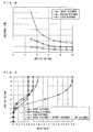
- Fig. 6 is a graph showing a relation between brightness and a response speed. Specifically, in Fig. 6 , a filled square sign represents the liquid crystal display element 10 according to the present embodiment and an unfilled diamond-shaped sign represents a conventional liquid crystal display element.
- the liquid crystal display element 10 according to the present embodiment was able to obtain a faster response characteristic in the entire brightness region (entire luminance region) than that of the conventional liquid crystal display element, by employing the driving as described above with reference to Fig. 5 .
- the liquid crystal display element 10 according to the present embodiment can have improved response speeds in the entire luminance region, in other words, in the entire gray scale region.
- the driving of the liquid crystal display element 10 according to the present embodiment is carried out based on the following principles.
- response time tends to be long although a transmittance is high.
- the portion In a case where a high voltage is applied in the portion with the long electrode distance, the portion has a short response time and therefore has little problem even if driving is carried out with the same level of signal voltage as that for a portion where the electrode distance is short.
- the response time becomes very long. In view of this, by avoiding use of the portion with the long electrode distance in order to perform the display in the brightness region in which the portion with the long electrode distance has the long response time, it is possible to drive the portion with the long electrode distance while maintaining the short response time.
- a response speed is controlled by separately changing, according to the desired brightness in display to be carried out, (i) a voltage to be supplied to the sub-picture element with the short electrode distance and (ii) a voltage to be supplied to the sub-picture element with the long electrode distance.
- the voltages to be applied to the sub-picture elements 22 are made different from each other according to desired brightness in display to be carried out.
- two signal electrode lines 42 are provided to each picture element 20, and different signal voltages are applied to the sub-picture element 22 having a small interdigital distance (electrode distance) and to the sub-picture element 22 having a long interdigital distance.
- electrode distance electrode distance
- the sub-picture element 22 having the long interdigital distance so as to apply, to each of the sub-picture elements 22, a voltage that may achieve as a fast response speed as possible.
- by applying voltages to the sub-picture elements 22 in the above-described manner it becomes possible to improve a response speed especially around brightness of the middle gray scale.
- Fig. 7 is a schematic view of a liquid crystal display element 10 according to the present embodiment.
- the liquid crystal display element 10 according to the present embodiment is different from the liquid crystal display element 10 according to Embodiment 1 in that the liquid crystal display element 10 according to the present embodiment includes a picture element 20 that is divided up into three sub-picture elements 22.
- one picture element 20 is divided up into the first sub-picture element 22a in which the electrode distance is long and the second sub-picture element 22b in which the electrode distance is short, as illustrated in Fig. 1 .
- each gray scale picture element 20 is divided up into a first sub-picture element 22a and a third sub-picture element 22c in each of which the electrode distance is long, and a second sub-picture element 22b in which the electrode distance is short, as illustrated in Fig. 7 .
- the electrode distance in the first sub-picture element 22a is equal to that in the third sub-picture element 22c.
- the third sub-picture element 22c is provided in a region which corresponds to the region where the first sub-picture element 22a is provided in the liquid crystal display element 10 according to Embodiment 1. That is, the first sub-picture element 22a is reduced in size and the third sub-picture element 22c is provided in a region that has become available due to the reduction in size of the first sub-picture element 22a.
- a third picture element electrode 30c which is a picture element electrode 30 in the third sub-picture element 22c, extends from the picture element electrode main line portion 34 that extends from a drain electrode of the first TFT 50a, in a similar manner as the first picture element electrode 30a.
- the third picture element electrode 30c is an interleaved electrode like the first picture element electrode 30a etc., and has a third picture element electrode digit portion 32c that extends along the vertical direction.
- a common electrode 36 in the third sub-picture element 22c is an interleaved electrode like the third picture element electrode 30c.
- a third common electrode digit portion 38c which is a digit portion extending in a digit shape from the common signal line 44 along the vertical direction, is provided as the common electrode 36 in the third sub-picture element 22c.
- the electrode distance in the third sub-picture element 22c is a distance (a third distance d3 as shown in Fig. 7 ) between the third picture element electrode digit portion 32c and the third common electrode digit portion 38c.
- the third distance d3 is equal to the above described first distance d1.
- This configuration makes it possible to improve a viewing angle characteristic of the liquid crystal display element 10. This is because regions are provided in one picture element 20, in one (the third sub-picture element 22c) of which regions an orientation of electrodes is different from those of electrodes in the others (the first sub-picture element 22a and the second sub-picture element 22b) by 90 degrees.
- the first distance d1 which is an electrode distance in the first sub-picture element 22a
- the third distance d3 which is an electrode distance in the third sub-picture element 22c.
- the third distance d3 does not necessarily need to be equal to the first distance d1 but may be different therefrom.
- the electrode distance in the third sub-picture element 22c may take a value that is between the value of the electrode distance in the first sub-picture element 22a and the value of the electrode distance in the second sub-picture element 22b (such an electrode distance as in the third sub-picture element 22c may be hereinafter referred to as a middle electrode distance). That is, the third distance d3 may take a value that is between the values of the above-described first and second distances d1 and d2.
- a new TFT 50 for example, a third TFT or the like for driving the third sub-picture element 22c, be provided for the purpose of driving the third sub-picture element 22c independently of the first and second sub-picture elements 22a and 22b. In this way, a voltage to be applied to the third sub-picture element 22c can be separately controlled.
- Figs. 8 to 11 correspond to Figs. 3 to 6 , respectively.
- Fig. 8 shows a relation between an applied voltage and response time.
- Fig. 9 shows a relation between an applied voltage and brightness.
- Fig. 10 shows a relation between brightness and an applied voltage.
- Fig. 11 shows a relation between brightness and response time.
- Unfilled triangular signs in Figs. 8 to 10 each indicate a case where the electrode distance is middle.
- An unfilled circular sign in Fig. 9 indicates a value obtained by summing up a value in a region in which the electrode distance is long, a value in a region in which the electrode distance is middle, and a value in a region in which the electrode distance is short.
- a sub-picture element(s) 22 to be used for display is(are) switched over among the first sub-picture element 22a, the second sub-picture element 22b, and the third sub-picture element 22c as shown in Fig.
- the second sub-picture element 22b short electrode distance
- the third sub-picture element 22c middle electrode distance
- the first sub-picture element 22a long electrode distance
- simultaneous use of the first sub-picture element 22a long electrode distance
- second sub-picture element 22b short electrode distance
- simultaneous use of the first sub-picture element 22a long electrode distance
- simultaneous use of the first sub-picture element 22a long electrode distance
- third sub-picture element 22c simultaneous use of the first sub-picture element 22a (long electrode distance) and the third sub-picture element 22c (middle electrode distance
- simultaneous use of the first sub-picture element 22a long electrode distance
- the second sub-picture element 22b short electrode distance
- the third sub-picture element 22c third sub-picture element 22c
- liquid crystal display element 10 having the above-described configuration, it is possible to obtain a response time shortening effect around middle range brightness as shown in Fig. 11 , in a similar manner as the liquid crystal display element 10 according to Embodiment 1 as previously described with reference to Fig. 6 .
- Fig. 12 shows an example of a waveform applied to the liquid crystal display element 10 in a case where a counter voltage is AC driven.
- liquid crystal display element 10 it is possible to increase a signal voltage to be applied to each of the sub-picture elements 22, by AC driving a counter voltage signal that is a signal to be applied to the common signal line 44 in such a manner that the counter voltage signal has an opposite phase to that of the voltage to be applied to each of the sub-picture elements 22. Also, by carrying out driving in this manner, it is possible to further improve a response speed of the liquid crystal display element 10. This will be described in detail below with reference to Fig. 12 .
- Fig. 12 shows a signal signal voltage (Vs) to be applied to the signal electrode line 42, a counter voltage (Vcom) to be applied to the common signal line 44 (common electrode 36), and a scanning signal (Vg, Vgh: high, Vgl: low) to be applied to the scanning signal line 40.
- Fig. 12 shows an example in which a screen (frame) is formed by three lines in frame driving.
- first writing and second writing are performed respectively with voltages identical in amplitude but opposite in polarity so as to eliminate a DC component applied to a liquid crystal.
- the counter voltage is AC driven so that the counter voltage signal has a reverse polarity of that of a voltage to be applied to each of the sub-picture elements 22.
- a voltage to be applied to the liquid crystal has a value that is obtained by subtracting Vcom from Vs (A+B). This makes it possible to increase the voltage to be applied to the liquid crystal, so that a response speed of the liquid crystal display element 10 can be further improved.
- Fig. 13 is a schematic view of an entire configuration of the liquid crystal display element 10.
- the liquid crystal display element 10 has a liquid crystal display panel 12 in which the picture elements 20 are arranged in matrix, a display control section 60, a scanning signal control section 62 as a gate driver, a signal electrode control section 64 as a source driver, and a common electrode control section 66.
- the display control section 60 controls the scanning signal control section 62 and the signal electrode control section 64.
- the control of turning on the sub-picture elements 22 as described, for example, with reference to Fig. 5 or the like is carried out via the display control section 60 and the common electrode control section 66, in particular, via the signal electrode control section 64.
- the driving method as described, for example, with reference to Fig. 12 or the like is carried out via the display control section 60 and the common electrode control section 66, in particular, via the common electrode control section 66.
- an output ratio of the first sub-picture element 22a and the second sub-picture element 22b may be, but not limited to, such a ratio as 1:9 or 9:1, thereby making it possible to obtain a good viewing angle characteristic while obtaining an improved response speed at the same time.
- an area ratio of the sub-picture elements 22 in the liquid crystal display element 10 and Line/Space in the sub-picture elements 22 as described above are not limited in particular but allows various modifications.
- liquid crystal display element 10 there is no limitation in particular on a liquid crystal mode to be used in the liquid crystal display element 10.
- the liquid crystal display element 10 may be used, for example, with IPS or the like.
- the liquid crystal display element may be used as a display section so as to constitute various types of liquid crystal display devices such as a liquid crystal TV, a mobile terminal or the like.
- the low gray scale region is a gray scale region ranging from a minimum gray scale value to a gray scale value corresponding to an applied voltage with which luminance of the sub-picture element in which the distance is long is greater than luminance of the sub-picture element in which the distance is short, in a case where a same potential is applied to the sub-picture element in which the distance is short and to the sub-picture element in which the distance is long, the middle gray scale region is a gray scale region continuing from the low gray scale region to a highest gray scale value that is obtainable by luminance obtained solely by means of the sub-picture element in which the distance is long, and the high gray scale region is a gray scale region continuing from the middle gray scale region to a maximum gray scale value.
- the picture element in which the electrode distance is long and the picture element in which the electrode distance is short are compared with each other in terms of luminance (intensity of light per unit area), the following matter is observed. That is, in a gray scale region in which an applied voltage is low, the picture element in which the electrode distance is short has higher luminance than the picture element in which the electrode distance is long, and in a gray scale region in which an applied voltage is high, the picture element in which the electrode distance is long has higher luminance than the picture element in which the electrode distance is short.
- the low gray scale region is a gray scale region which corresponds to an applied voltage with which the sub-picture element in which the electrode distance is short has luminance higher than that of the sub-picture element in which the electrode distance is long in a case where the same potential is applied in both the sub-picture elements.
- the middle gray scale region is a gray scale region which continues from the low gray scale region and in which sufficient luminance is obtained solely by means of the sub-picture element in which the electrode distance is long.
- the middle gray scale region is a gray scale region ranging from a lower limit gray scale value of the middle gray scale region to an upper limit gray scale value of the middle gray scale region, wherein the lower limit gray scale value of the middle gray scale region is not less than 30% nor more than 45% of the maximum gray scale value and the upper limit gray scale value of the middle gray scale region is not less than 55% nor more than 70% of the maximum gray scale value, the low gray scale region is a gray scale region ranging from the minimum gray scale value to the lower limit gray scale value of the middle gray scale region, and the high gray scale region is a gray scale region ranging from the upper limit gray scale value of the middle gray scale region to the maximum gray scale value.
- This configuration makes it possible to easily set gray scale regions based on gray scale values. Specifically, based on gray scale regions, it is possible to set, as the low gray scale region, a region in which the sub-picture element in which the electrode distance is long has a slow response speed due to a low applied voltage. Also, based on gray scale values, it is possible to set, as the middle gray scale region, a region in which the sub-picture element in which the electrode distance is long has an increased response speed due to a relatively high applied voltage and in which region desired luminance can be obtained solely by means of the sub-picture element in which the electrode distance is long.
- liquid crystal display element according the present invention, display in the low gray scale region is carried out solely by means of the sub-picture element in which the distance is short, and display in the middle gray scale region is carried out solely by means of the sub-picture element in which the distance is long.
- each of the picture elements is divided up into at least three sub-picture elements, at least three of the sub-picture elements are each provided with a switching element, and when a sub-picture element which is among the sub-picture elements each provided with the switching element and in which the distance is between the distance of the sub-picture element in which the distance is short and the distance of the sub-picture element in which the distance is long is denoted as a sub-picture element in which the distance is middle, display in the middle gray scale region is carried out mainly by means of the sub-picture element in which the distance is short and the sub-picture element in which the distance is long, and display in the high gray scale region is carried out mainly by means of the sub-picture element in which the distance is middle, the sub-picture element in which the distance is short, and the sub-picture element in which the distance is long.
- each of the picture elements is provided with a plurality of signal electrode lines so that different voltages can be supplied to the sub-picture elements, respectively.
- This configuration makes it possible to independently drive each sub-picture element with a different applied voltage.
- each of the picture elements is provided with a common signal line which is connected to the common electrode and is common to the sub-picture elements of the picture element.
- This configuration makes it possible to easily provide, in each of the sub-picture elements, a configuration in which driving is carried out between the picture element electrode and the common electrode. This makes it easy for a potential difference between the picture element electrode and the common electrode to be different between the sub-picture elements.
- the picture element electrodes are formed to interleave with the common electrode.
- This configuration makes it easy to set the electrode distances and to reduce the electrode distances. This makes it easy to improve the response speed.
- the sub-picture elements in each picture element are different in directions along which digits of the picture element electrode and the digit-shaped common electrode extend.
- a direction along which a digit portion extends differs between the sub-picture elements. Due to this, regions are formed in a pixel, in each of which regions an orientation of liquid crystal molecules is different from that of liquid crystal molecules in the other regions.
- an upper limit gray scale value of the low gray scale region is so set that a response speed of a desired value or less is obtainable after display in the low gray scale region is switched to display in the middle gray scale region; and an/the upper limit gray scale value of the middle gray scale region is so set that a response speed of a desired value or less is obtainable after display in the middle gray scale region is switched to display in the high gray scale region.
- This configuration makes it possible to satisfy a desired response speed in the entire gray scale region, which response speed is determined, for example, based on a product specification or the like.
- this configuration increases a range of brightness within which range a plurality of sub-picture elements are driven at the same time, thereby making it possible to improve a viewing angle characteristic.
- a counter voltage to be applied to the common electrode is reversed for every frame in frame driving, and the counter voltage is opposite in phase to a voltage to be applied to the picture element electrode.
- This configuration can increase a voltage to be applied to liquid crystal molecules, thereby further improving the response speed.
- a liquid crystal display device includes the liquid crystal display element as a display section.
- the present invention can be suitably applied to a display device for which a fast response speed is required, for example, to a liquid crystal TV or the like.
Landscapes
- Physics & Mathematics (AREA)
- Engineering & Computer Science (AREA)
- Nonlinear Science (AREA)
- Crystallography & Structural Chemistry (AREA)
- General Physics & Mathematics (AREA)
- Chemical & Material Sciences (AREA)
- Computer Hardware Design (AREA)
- Theoretical Computer Science (AREA)
- Microelectronics & Electronic Packaging (AREA)
- Mathematical Physics (AREA)
- Optics & Photonics (AREA)
- Liquid Crystal (AREA)
- Control Of Indicators Other Than Cathode Ray Tubes (AREA)
- Liquid Crystal Display Device Control (AREA)
Applications Claiming Priority (2)
| Application Number | Priority Date | Filing Date | Title |
|---|---|---|---|
| JP2009131555 | 2009-05-29 | ||
| PCT/JP2010/001416 WO2010137209A1 (fr) | 2009-05-29 | 2010-03-02 | Élément d'affichage à cristaux liquides, dispositif d'affichage à cristaux liquides et procédé d'affichage d'élément d'affichage à cristaux liquides |
Publications (2)
| Publication Number | Publication Date |
|---|---|
| EP2437109A1 true EP2437109A1 (fr) | 2012-04-04 |
| EP2437109A4 EP2437109A4 (fr) | 2012-12-05 |
Family
ID=43222343
Family Applications (1)
| Application Number | Title | Priority Date | Filing Date |
|---|---|---|---|
| EP10780172A Withdrawn EP2437109A4 (fr) | 2009-05-29 | 2010-03-02 | Élément d'affichage à cristaux liquides, dispositif d'affichage à cristaux liquides et procédé d'affichage d'élément d'affichage à cristaux liquides |
Country Status (6)
| Country | Link |
|---|---|
| US (1) | US8669973B2 (fr) |
| EP (1) | EP2437109A4 (fr) |
| JP (1) | JP5220921B2 (fr) |
| CN (1) | CN102292666A (fr) |
| RU (1) | RU2011132280A (fr) |
| WO (1) | WO2010137209A1 (fr) |
Families Citing this family (13)
| Publication number | Priority date | Publication date | Assignee | Title |
|---|---|---|---|---|
| KR20120056110A (ko) * | 2010-11-24 | 2012-06-01 | 삼성모바일디스플레이주식회사 | 액정 표시 장치 및 그 반전 구동 방법 |
| TWI435153B (zh) | 2010-12-28 | 2014-04-21 | Au Optronics Corp | 畫素結構 |
| TWI412858B (zh) * | 2010-12-29 | 2013-10-21 | Au Optronics Corp | 畫素結構 |
| CN202487576U (zh) | 2012-02-09 | 2012-10-10 | 京东方科技集团股份有限公司 | 阵列基板和双视场显示装置 |
| CN102629041B (zh) | 2012-02-09 | 2014-04-16 | 京东方科技集团股份有限公司 | 一种3d显示装置及其制造方法 |
| CN102929054B (zh) | 2012-11-05 | 2015-03-25 | 京东方科技集团股份有限公司 | 一种阵列基板及像素的驱动方法 |
| CN103901684B (zh) * | 2012-12-28 | 2018-02-09 | 上海中航光电子有限公司 | 一种ips模式的液晶显示器 |
| CN103941498B (zh) * | 2013-11-15 | 2016-12-14 | 上海中航光电子有限公司 | 一种tft阵列基板、显示面板和显示装置 |
| CN104317084B (zh) * | 2014-11-07 | 2017-05-17 | 深圳市华星光电技术有限公司 | 液晶面板及其驱动方法 |
| WO2018191910A1 (fr) * | 2017-04-20 | 2018-10-25 | Boe Technology Group Co., Ltd. | Panneau d'affichage à cristaux liquides, appareil d'affichage à cristaux liquides et son procédé de fonctionnement |
| CN106873264A (zh) * | 2017-04-27 | 2017-06-20 | 厦门天马微电子有限公司 | 阵列基板、液晶显示面板、显示装置和像素充电方法 |
| CN106932976A (zh) * | 2017-05-05 | 2017-07-07 | 京东方科技集团股份有限公司 | 显示装置、阵列基板及像素单元 |
| KR102593430B1 (ko) * | 2018-07-09 | 2023-10-26 | 삼성디스플레이 주식회사 | 발광 장치 및 이를 구비한 표시 장치 |
Family Cites Families (16)
| Publication number | Priority date | Publication date | Assignee | Title |
|---|---|---|---|---|
| JPH06148596A (ja) | 1992-10-30 | 1994-05-27 | Hitachi Ltd | アクティブマトリクス型液晶表示装置 |
| JPH10319369A (ja) | 1997-05-16 | 1998-12-04 | Hitachi Ltd | 薄膜トランジスタ液晶表示装置 |
| JP3479696B2 (ja) * | 1997-12-08 | 2003-12-15 | ビオイ−ハイディス テクノロジー カンパニー リミテッド | 液晶表示装置 |
| JP3805966B2 (ja) * | 1999-10-21 | 2006-08-09 | 松下電器産業株式会社 | 液晶表示装置 |
| KR100433596B1 (ko) | 1999-10-21 | 2004-05-31 | 마쯔시다덴기산교 가부시키가이샤 | 액정표시장치 |
| TWI280547B (en) | 2000-02-03 | 2007-05-01 | Samsung Electronics Co Ltd | Liquid crystal display and driving method thereof |
| JP4002105B2 (ja) * | 2002-01-15 | 2007-10-31 | 株式会社日立製作所 | 液晶表示装置 |
| CN101393362B (zh) * | 2003-07-14 | 2012-04-11 | 株式会社日立显示器 | 显示装置 |
| JP4082683B2 (ja) * | 2003-09-29 | 2008-04-30 | 株式会社 日立ディスプレイズ | 半透過型液晶表示装置 |
| JP4394512B2 (ja) * | 2004-04-30 | 2010-01-06 | 富士通株式会社 | 視角特性を改善した液晶表示装置 |
| JP4754205B2 (ja) * | 2004-05-17 | 2011-08-24 | パナソニック株式会社 | プラズマディスプレイ装置及びプラズマディスプレイパネルの駆動方法 |
| KR101100882B1 (ko) | 2004-11-05 | 2012-01-02 | 삼성전자주식회사 | 액정 표시 장치 및 그 구동 장치 |
| JP2006201594A (ja) | 2005-01-21 | 2006-08-03 | Sharp Corp | 液晶表示装置 |
| JP4453694B2 (ja) * | 2006-10-31 | 2010-04-21 | セイコーエプソン株式会社 | 液晶装置及び電子機器 |
| KR101348755B1 (ko) * | 2007-04-04 | 2014-01-07 | 삼성디스플레이 주식회사 | 디스플레이장치 및 그 제어방법 |
| JP4989309B2 (ja) | 2007-05-18 | 2012-08-01 | 株式会社半導体エネルギー研究所 | 液晶表示装置 |
-
2010
- 2010-03-02 US US13/148,508 patent/US8669973B2/en not_active Expired - Fee Related
- 2010-03-02 JP JP2011515844A patent/JP5220921B2/ja not_active Expired - Fee Related
- 2010-03-02 EP EP10780172A patent/EP2437109A4/fr not_active Withdrawn
- 2010-03-02 RU RU2011132280/28A patent/RU2011132280A/ru not_active Application Discontinuation
- 2010-03-02 WO PCT/JP2010/001416 patent/WO2010137209A1/fr not_active Ceased
- 2010-03-02 CN CN2010800051963A patent/CN102292666A/zh active Pending
Also Published As
| Publication number | Publication date |
|---|---|
| JPWO2010137209A1 (ja) | 2012-11-12 |
| CN102292666A (zh) | 2011-12-21 |
| RU2011132280A (ru) | 2013-07-10 |
| JP5220921B2 (ja) | 2013-06-26 |
| US8669973B2 (en) | 2014-03-11 |
| US20110316843A1 (en) | 2011-12-29 |
| WO2010137209A1 (fr) | 2010-12-02 |
| EP2437109A4 (fr) | 2012-12-05 |
Similar Documents
| Publication | Publication Date | Title |
|---|---|---|
| US8669973B2 (en) | Liquid crystal display element, liquid crystal display device, and method for displaying with liquid crystal display element | |
| JP5414974B2 (ja) | 液晶表示装置 | |
| CN107505782B (zh) | 阵列基板和液晶显示装置及驱动方法 | |
| CN101960371B (zh) | 有源矩阵基板、液晶面板、液晶显示装置、液晶显示单元、以及电视接收机 | |
| US20170263170A1 (en) | Array Substrate, Display Device and Driving Method Thereof | |
| US7764262B2 (en) | Liquid crystal display device and method of driving the same | |
| US20100245326A1 (en) | Common electrode drive circuit and liquid crystal display | |
| KR101944482B1 (ko) | 표시 패널 및 이의 구동 방법 | |
| KR101725341B1 (ko) | 액정 표시 장치 | |
| CN107861278B (zh) | 液晶显示装置 | |
| CN107490884B (zh) | 选择器、阵列基板和液晶显示装置及驱动方法 | |
| CN100472291C (zh) | 液晶显示器 | |
| EP2846184B1 (fr) | Substrat matriciel, panneau d'affichage à cristaux liquides et dispositif d'affichage | |
| CN108389557B (zh) | 显示装置及其驱动方法 | |
| US20160351137A1 (en) | Display device | |
| KR101122002B1 (ko) | 액정 표시 패널 및 그 구동 방법 | |
| US20120007843A1 (en) | Tft substrate and liquid crystal display apparatus using the same | |
| JP2009223167A (ja) | 液晶表示装置 | |
| GB2489295A (en) | Liquid crystal display device and method of driving the same | |
| CN102654988A (zh) | 液晶显示器驱动电路、液晶显示区及其驱动方法 | |
| JP2010026324A (ja) | 液晶表示パネル、液晶表示ユニット、液晶表示装置、テレビジョン受像機 | |
| JP2005189614A (ja) | 液晶表示装置 | |
| JP3650280B2 (ja) | 横電界型アクティブマトリクス液晶表示装置 | |
| RU2653769C1 (ru) | Жидкокристаллическая 3d панель с технологией "невооруженным глазом" и способ управления такой панелью | |
| KR100949499B1 (ko) | 액정표시장치의 구동방법 및 그의 구동회로 |
Legal Events
| Date | Code | Title | Description |
|---|---|---|---|
| PUAI | Public reference made under article 153(3) epc to a published international application that has entered the european phase |
Free format text: ORIGINAL CODE: 0009012 |
|
| 17P | Request for examination filed |
Effective date: 20110805 |
|
| AK | Designated contracting states |
Kind code of ref document: A1 Designated state(s): AT BE BG CH CY CZ DE DK EE ES FI FR GB GR HR HU IE IS IT LI LT LU LV MC MK MT NL NO PL PT RO SE SI SK SM TR |
|
| DAX | Request for extension of the european patent (deleted) | ||
| A4 | Supplementary search report drawn up and despatched |
Effective date: 20121106 |
|
| RIC1 | Information provided on ipc code assigned before grant |
Ipc: G02F 1/133 20060101ALI20121030BHEP Ipc: G02F 1/1343 20060101AFI20121030BHEP Ipc: G09G 3/20 20060101ALI20121030BHEP Ipc: G09G 3/36 20060101ALI20121030BHEP |
|
| GRAP | Despatch of communication of intention to grant a patent |
Free format text: ORIGINAL CODE: EPIDOSNIGR1 |
|
| INTG | Intention to grant announced |
Effective date: 20150901 |
|
| STAA | Information on the status of an ep patent application or granted ep patent |
Free format text: STATUS: THE APPLICATION IS DEEMED TO BE WITHDRAWN |
|
| 18D | Application deemed to be withdrawn |
Effective date: 20160112 |