EP2437321A2 - Leuchtdiodenbaugruppenstruktur und Herstellungsverfahren dafür - Google Patents
Leuchtdiodenbaugruppenstruktur und Herstellungsverfahren dafür Download PDFInfo
- Publication number
- EP2437321A2 EP2437321A2 EP11167682A EP11167682A EP2437321A2 EP 2437321 A2 EP2437321 A2 EP 2437321A2 EP 11167682 A EP11167682 A EP 11167682A EP 11167682 A EP11167682 A EP 11167682A EP 2437321 A2 EP2437321 A2 EP 2437321A2
- Authority
- EP
- European Patent Office
- Prior art keywords
- electrically conductive
- fluorescent substrate
- fluorescent
- substrate
- led
- Prior art date
- Legal status (The legal status is an assumption and is not a legal conclusion. Google has not performed a legal analysis and makes no representation as to the accuracy of the status listed.)
- Withdrawn
Links
Images







Classifications
-
- H—ELECTRICITY
- H10—SEMICONDUCTOR DEVICES; ELECTRIC SOLID-STATE DEVICES NOT OTHERWISE PROVIDED FOR
- H10H—INORGANIC LIGHT-EMITTING SEMICONDUCTOR DEVICES HAVING POTENTIAL BARRIERS
- H10H20/00—Individual inorganic light-emitting semiconductor devices having potential barriers, e.g. light-emitting diodes [LED]
- H10H20/80—Constructional details
- H10H20/85—Packages
- H10H20/857—Interconnections, e.g. lead-frames, bond wires or solder balls
-
- H—ELECTRICITY
- H10—SEMICONDUCTOR DEVICES; ELECTRIC SOLID-STATE DEVICES NOT OTHERWISE PROVIDED FOR
- H10H—INORGANIC LIGHT-EMITTING SEMICONDUCTOR DEVICES HAVING POTENTIAL BARRIERS
- H10H20/00—Individual inorganic light-emitting semiconductor devices having potential barriers, e.g. light-emitting diodes [LED]
- H10H20/01—Manufacture or treatment
- H10H20/036—Manufacture or treatment of packages
- H10H20/0364—Manufacture or treatment of packages of interconnections
-
- H—ELECTRICITY
- H10—SEMICONDUCTOR DEVICES; ELECTRIC SOLID-STATE DEVICES NOT OTHERWISE PROVIDED FOR
- H10H—INORGANIC LIGHT-EMITTING SEMICONDUCTOR DEVICES HAVING POTENTIAL BARRIERS
- H10H20/00—Individual inorganic light-emitting semiconductor devices having potential barriers, e.g. light-emitting diodes [LED]
- H10H20/80—Constructional details
- H10H20/85—Packages
- H10H20/8506—Containers
-
- H—ELECTRICITY
- H10—SEMICONDUCTOR DEVICES; ELECTRIC SOLID-STATE DEVICES NOT OTHERWISE PROVIDED FOR
- H10H—INORGANIC LIGHT-EMITTING SEMICONDUCTOR DEVICES HAVING POTENTIAL BARRIERS
- H10H20/00—Individual inorganic light-emitting semiconductor devices having potential barriers, e.g. light-emitting diodes [LED]
- H10H20/80—Constructional details
- H10H20/85—Packages
- H10H20/851—Wavelength conversion means
- H10H20/8511—Wavelength conversion means characterised by their material, e.g. binder
- H10H20/8512—Wavelength conversion materials
- H10H20/8513—Wavelength conversion materials having two or more wavelength conversion materials
-
- H—ELECTRICITY
- H10—SEMICONDUCTOR DEVICES; ELECTRIC SOLID-STATE DEVICES NOT OTHERWISE PROVIDED FOR
- H10H—INORGANIC LIGHT-EMITTING SEMICONDUCTOR DEVICES HAVING POTENTIAL BARRIERS
- H10H20/00—Individual inorganic light-emitting semiconductor devices having potential barriers, e.g. light-emitting diodes [LED]
- H10H20/80—Constructional details
- H10H20/85—Packages
- H10H20/851—Wavelength conversion means
- H10H20/8515—Wavelength conversion means not being in contact with the bodies
-
- H—ELECTRICITY
- H10—SEMICONDUCTOR DEVICES; ELECTRIC SOLID-STATE DEVICES NOT OTHERWISE PROVIDED FOR
- H10W—GENERIC PACKAGES, INTERCONNECTIONS, CONNECTORS OR OTHER CONSTRUCTIONAL DETAILS OF DEVICES COVERED BY CLASS H10
- H10W72/00—Interconnections or connectors in packages
- H10W72/50—Bond wires
- H10W72/531—Shapes of wire connectors
- H10W72/536—Shapes of wire connectors the connected ends being ball-shaped
-
- H—ELECTRICITY
- H10—SEMICONDUCTOR DEVICES; ELECTRIC SOLID-STATE DEVICES NOT OTHERWISE PROVIDED FOR
- H10W—GENERIC PACKAGES, INTERCONNECTIONS, CONNECTORS OR OTHER CONSTRUCTIONAL DETAILS OF DEVICES COVERED BY CLASS H10
- H10W72/00—Interconnections or connectors in packages
- H10W72/50—Bond wires
- H10W72/531—Shapes of wire connectors
- H10W72/5363—Shapes of wire connectors the connected ends being wedge-shaped
-
- H—ELECTRICITY
- H10—SEMICONDUCTOR DEVICES; ELECTRIC SOLID-STATE DEVICES NOT OTHERWISE PROVIDED FOR
- H10W—GENERIC PACKAGES, INTERCONNECTIONS, CONNECTORS OR OTHER CONSTRUCTIONAL DETAILS OF DEVICES COVERED BY CLASS H10
- H10W90/00—Package configurations
-
- H—ELECTRICITY
- H10—SEMICONDUCTOR DEVICES; ELECTRIC SOLID-STATE DEVICES NOT OTHERWISE PROVIDED FOR
- H10W—GENERIC PACKAGES, INTERCONNECTIONS, CONNECTORS OR OTHER CONSTRUCTIONAL DETAILS OF DEVICES COVERED BY CLASS H10
- H10W90/00—Package configurations
- H10W90/701—Package configurations characterised by the relative positions of pads or connectors relative to package parts
- H10W90/751—Package configurations characterised by the relative positions of pads or connectors relative to package parts of bond wires
- H10W90/754—Package configurations characterised by the relative positions of pads or connectors relative to package parts of bond wires between a chip and a stacked insulating package substrate, interposer or RDL
Definitions
- the present disclosure relates to a semiconductor package structure and a manufacturing method thereof. More particularly, the present disclosure relates to a light emitting diode (LED) package structure and a manufacturing method thereof.
- LED light emitting diode
- LEDs generally offer a number of advantageous characteristics such as long product life, compact size, high shock resistance, low heat generation and low power consumption, etc. As a result LEDs are widely employed in household applications and as the light source or indicator of a variety of equipment. Recent developments of new LEDs are in the areas of multiple colors and high brightness. Accordingly, LEDs are further employed in applications such as large outdoor bulletin boards, traffic signals and related fields. In the future, LEDs may even become the primary light source for illumination that not only conserve electricity but also are environmentally friendly.
- a type of white-light LED is composed of a blue-light LED chip and yellow phosphor.
- a prior art manufacturing method of a white-light LED package structure typically disposes a blue-light LED chip on a base and wire bonds the blue-light LED chip with the base. Afterwards, using spin coating, dispensing, spray coating, molding or any other suitable process on the base, a yellow fluorescent layer is formed on the blue-light LED chip. A portion of the yellow fluorescent layer emits yellow light upon excitation by the blue light emitted by the blue-light LED chip, and in turn the yellow light, combined with the blue light emitted by the blue-light LED chip, produces white light.
- a yellow fluorescent layer formed by spin coating, dispensing, spray coating or the like tends to suffer from excessive usage of phosphor powder and results in uneven thickness of the layer. That is, when the blue light emitted by the blue-light LED chip traverses through a yellow fluorescent layer of a greater thickness, the white-light LED package structure may produce a yellowish halo, causing the color of the light emitted by the LED package structure to be uneven overall.
- U.S. Patent No. 6,395,564 and U.S. Patent Publication No. 2009/261358 disclose a technique that involves spraying the fluorescent layer directly on wafers and forming white-light LED package structures after cutting the wafers.
- Such prior art technique suffers from the problem of lowered scattering efficiency during the process of the yellow fluorescent layer emitting yellow light upon excitation by the blue light.
- manufacturing costs tend to increase if the difference in wavelengths is to be rectified by way of spin-coating fluorescent layer on wafers.
- U.S. Patent No. 6,630,691 discloses a manufacturing method of a phosphor layer. Ceramic glass and phosphor are combined under high temperature to result in a eutectic process that forms a fluorescent substrate, which is pasted to LED chips to avoid the issue of low scattering efficiency and enhance the uniformity of light generated by the LED package structure.
- a phosphor layer Ceramic glass and phosphor are combined under high temperature to result in a eutectic process that forms a fluorescent substrate, which is pasted to LED chips to avoid the issue of low scattering efficiency and enhance the uniformity of light generated by the LED package structure.
- the use of this technique is limited to flip chip LED chips.
- the present disclosure provides an LED package structure and a manufacturing method thereof that can help enhance the uniformity in the color of light generated by LED chips.
- an LED package structure may comprise a fluorescent substrate, a first electrically conductive pattern, a second electrically conductive pattern, at least one electrically conductive component, and an LED chip.
- the fluorescent substrate may have a first surface and a second surface opposite the first surface.
- the fluorescent substrate may comprise a fluorescent material and a glass material.
- the first electrically conductive pattern may be disposed on the first surface of the fluorescent substrate.
- the second electrically conductive pattern may be disposed on the second surface of the fluorescent substrate.
- the at least one electrically conductive component may connect the first electrically conductive pattern and the second electrically conductive pattern.
- the LED chip may be disposed on the second surface of the fluorescent substrate.
- the LED chip may have a light extraction surface coupled to the second electrically conductive pattern such that the LED chip is electrically coupled to the first electrically conductive pattern via the at least one electrically conductive component.
- a thickness of the fluorescent substrate may be substantially constant throughout the fluorescent substrate.
- the fluorescent material may comprise yellow phosphor.
- the fluorescent material may comprise phosphors of at least two different wavelengths.
- the phosphors may comprise at least two of yellow phosphor, red phosphor, and green phosphor.
- the LED package structure may further comprise an underfill disposed between the light extraction surface of the LED chip and the second surface of the fluorescent substrate, the underfill covering at least partially the light extraction surface of the LED chip.
- the underfill may cover a plurality of side surfaces of the LED chip.
- the LED chip may comprise a sapphire substrate.
- the LED package structure may further comprise a circuit board where a back surface of the LED chip opposite the light extraction surface is disposed on the circuit board. In one embodiment, the LED package structure may further comprise at least one bonding wire that electrically couples the circuit board and the first electrically conductive pattern.
- a manufacturing method of an LED package structure may comprise: providing a fluorescent substrate having a first surface and a second surface opposite the first surface, the fluorescent substrate containing therein a plurality of electrically conductive components that connect the first surface and the second surface, the fluorescent substrate comprising a mixture of at least one fluorescent material and a glass material; forming a first electrically conductive pattern on the first surface and a second electrically conductive pattern on the second surface, at least some of the electrically conductive components connecting the first electrically conductive pattern and the second electrically conductive pattern; and bonding a plurality of LED chips on the second surface of the fluorescent substrate, each of the LED chips having a respective light extraction surface coupled to the second electrically conductive pattern, each of the LED chips electrically coupled to the first electrically conductive pattern via a corresponding one of the electrically conductive components.
- the plurality of electrically conductive components may be formed by: forming a plurality of through holes in the fluorescent substrate, the through holes connecting the first surface and the second surface; electroplating the through holes to form a plurality of electrically conductive pillars protruding out of the first surface of the fluorescent substrate; polishing the electrically conductive pillars to provide the electrically conductive components that are flush with the first surface of the fluorescent substrate.
- the polishing comprises cutting the fluorescent substrate with a cutting device to reduce a thickness of the fluorescent substrate and to expose the electrically conductive components.
- the plurality of electrically conductive components may be formed by: forming a plurality of electrically conductive bumps in a recess of a supporting substrate; filling the recess of the supporting substrate with the at least one fluorescent material and the glass material, the at least one fluorescent material and the glass material covering the electrically conductive bumps; heating the electrically conductive bumps, the at least one fluorescent material, and the glass material together to form the fluorescent substrate with the electrically conductive bumps buried therein; and polishing the fluorescent substrate and the electrically conductive bumps to form the electrically conductive components that are flush with the first surface of the fluorescent substrate.
- the method may further comprise: forming a plurality of circuit boards on the second surface after forming the second electrically conductive pattern, the circuit boards connecting the second electrically conductive pattern.
- the method may further comprise: forming an underfill between the light extraction surface of the LED chips and the second surface of the fluorescent substrate after bonding the LED chips on the second surface of the fluorescent substrate, the underfill covering at least partially the light extraction surface of the LED chips.
- the method may additionally comprise: after forming the underfill, carrying out a cutting process to form a plurality of LED package structures.
- the underfill may cover at least partially a plurality of side surfaces of the LED chips.
- the method may also comprise: after forming the underfill, carrying out a cutting process to form a plurality of LED package structures.
- Figure 1A illustrates a cross-sectional view of an LED package structure in accordance with an embodiment of the present disclosure.
- Figure 1B illustrates a cross-sectional view of an LED package structure in accordance with another embodiment of the present disclosure.
- Figure 1C illustrates a cross-sectional view of an LED package structure in accordance with yet another embodiment of the present disclosure.
- Figure 2A illustrates a cross-sectional view of an LED package structure in accordance with still another embodiment of the present disclosure.
- Figure 2B illustrates a cross-sectional view of an LED package structure in accordance with a further embodiment of the present disclosure.
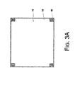
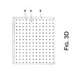
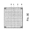
- FIGS. 3A through 3l illustrate a process of manufacturing an LED package structure in accordance with an embodiment of the present disclosure.
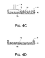
- FIGS. 4A through 4D illustrate a process of manufacturing of an electrically conductive component in accordance with an embodiment of the present disclosure.
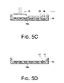
- FIGS. 5A through 5D illustrate a process of manufacturing of an electrically conductive component in accordance with another embodiment of the present disclosure.
- Figure 1A illustrates a cross-sectional view of an LED package structure in accordance with an embodiment of the present disclosure.
- the LED package structure 100a comprises a fluorescent substrate 110, a first electrically conductive pattern 120, a second electrically conductive pattern 130, at least one electrically conductive component 140a (only one being representatively illustrated in Figure 1A ), and an LED chip 150.
- the fluorescent substrate 110 comprises two opposite surfaces: a first surface 112 and a second surface 114.
- the fluorescent substrate 110 is composed of, for example, a mixture of a fluorescent material and a glass material.
- the fluorescent substrate 110 generally has a uniform thickness throughout.
- the first electrically conductive pattern 120 is disposed on the first surface 112 of the fluorescent substrate 110.
- the fluorescent material of the fluorescent substrate 110 may be, for example, a yellow fluorescent material, there are other types of fluorescent material and fluorescent materials of two or more different colors may be utilized. For example, yellow phosphor and red phosphor may be combined, green phosphor and red phosphor may be combined, and so on.
- the second electrically conductive pattern 130 is disposed on the second surface 114 of the fluorescent substrate 110.
- the electrically conductive component 140a traverses through the fluorescent substrate 110, connecting the first electrically conductive pattern 120 and the second electrically conductive pattern 130.
- the LED chip 150 is disposed on a side of the second surface 114 of the fluorescent substrate 110 and has a light extraction surface 152 which is connected to the second electrically conductive pattern 130. This allows the LED chip 150 to be electrically coupled to an external component (not illustrated) via an electrically conductive path formed by the second electrically conductive pattern 130, the electrically conductive component 140a, and the first electrically conductive pattern 120.
- the LED chip 150 in one embodiment may be a vertical emission LED chip, other LED chips with equivalent light emission characteristics are also within the scope of the present disclosure. For example, high-voltage LED chips or alternating current (AC) LED chips are also applicable.
- the electrically conductive component 140a allows a maximized density of three-dimensional stacking and minimized dimensions of the LED chip 150. Accordingly, signals between the fluorescent substrate 110 and the LED chip 150 can be passed through the electrically conductive component 140a, resulting in increased component speed, reduced signal delay, and lower power consumption.
- the LED package structure 110a further comprises an underfill 160a.
- the underfill 160a is disposed between the light extraction surface 152 of the LED chip 150 and the second surface 114 of the fluorescent substrate 110.
- the underfill 160a covers the light extraction surface 152 of the LED chip 150.
- functions of the underfill 160a include protecting the light extraction surface 152 of the LED chip 150 and avoiding total reflection of the light emitted by the LED chip 150 in the gap between the fluorescent substrate 110 and the LED chip 150, thereby enhancing the illumination efficiency of the LED package structure 100a.
- the underfill 160a is made of a material that comprises epoxy such as, for example and not limited to, silicone or silica gel, epoxy resin, or a compound thereof.
- the underfill 160a may further comprise a fluorescent material as an additive that is different than the fluorescent material in the fluorescent substrate 110.
- the fluorescent material of the underfill 160a may comprise red phosphor.
- the fluorescent material of the underfill 160a may comprise red phosphor/green phosphor. In this way, the color saturation of the LED package structure 110a can be enhanced.
- each LED chip 150 is configured to be used with the fluorescent substrate 110 that comprises a mixture of a fluorescent material and a glass material, that the first electrically conductive pattern 120, the second electrically conductive pattern 130 and the electrically conductive component 140 are disposed on the fluorescent substrate 110, and that each LED chip 150 is a selected one that generates a desired wavelength, a plurality of such LED chips 150 can thus produce light with wavelengths that fall within the same range.
- the fluorescent substrate 110 of the LED package structure has a uniform thickness, light emitted by the LED chip 150 passing through the fluorescent substrate 110 can be converted into a light with high uniformity.
- a plurality of such LED package structures can thus produce white light with wavelengths that fall within substantially the same range.
- the LED package structure 110a according to the present disclosure can produce light with better uniformity.
- FIG. 1B illustrates a cross-sectional view of an LED package structure in accordance with another embodiment of the present disclosure.
- the LED package structure 100a' of Figure 1B and the LED package structure 100a of Figure 1A are similar with one main difference being that in the LED package structure 100a' of Figure 1B a plurality of circuit boardcircuit boards 135 are disposed on the second surface 114 of the fluorescent substrate 110.
- the LED package structure 100a' comprises a plurality of first electrically conductive patterns 120, a plurality of second electrically conductive patterns 130, a plurality of electrically conductive components 140, and a plurality of LED chips 150.
- the second electrically conductive patterns 130 associated with the LED chips 150 are electrically coupled to one another via the circuit boardcircuit boards 135, and a variety of circuit designs can be configured depending on the needs. That is, depending on the needs of a user of the LED package structure 100a', there can be different circuit designs configured and implemented on the fluorescent substrate 110 to allow the user to efficiently achieve the desired results having the LED chips 150 connected in series or in parallel.
- FIG. 1C illustrates a cross-sectional view of an LED package structure in accordance with yet another embodiment of the present disclosure.
- the LED package structure 100a" of Figure 1C and the LED package structure 100a' of Figure 1B are similar with one main difference being that the LED package structure 100a" of Figure 1C further comprises a circuit boardcircuit board 170 and at least one bonding wire 180.
- the actual number of bonding wires 180 is not limited to that illustrated in Figure 1C and is determined according to the actual circuit implemented on the fluorescent substrate 110.
- the LED package structure 100a" of the illustrated embodiment is disposed on the circuit board 170, and a back surface 154 opposite the light extraction surface 152 of each of the LED chips 150 is disposed on the circuit board 170.
- the LED package structure 100a" is electrically coupled to the first electrically conductive patterns 120 and the circuit board 170 via the bonding wires 180. As such, the LED chips 150 can be electrically coupled to an external circuit (not illustrated) via the circuit board 170, thereby increasing the applicability of the LED package structure 100a".
- FIG 2A illustrates a cross-sectional view of an LED package structure in accordance with still another embodiment of the present disclosure.
- the LED package structure 100b of Figure 2A and the LED package structure 100a' of Figure 1B are similar with one main difference being that in the LED package structure 100b of Figure 2A the underfill 160b is extended to at least partially cover a plurality of side surfaces 156 of the LED chips 150.
- the LED chips 150 may each comprise a sapphire substrate, leakage of light or total reflection can be avoided with the side surfaces 156 of the LED chips 150 covered by the underfill 160a. This enhances the illumination efficiency of the LED package structure 100b.
- FIG. 2B illustrates a cross-sectional view of an LED package structure in accordance with a further embodiment of the present disclosure.
- the LED package structure 100b' of Figure 2B and the LED package structure 100b of Figure 2A are similar with one main difference being that the LED package structure 100b' of Figure 2B further comprises a circuit board 170 and at least one bonding wire 180 (only two being illustrated in Figure 2B ).
- a back surface 154 opposite the light extraction surface 152 of each of the LED chips 150 is disposed on the circuit board 170.
- the circuit board 170 is electrically coupled to the first electrically conductive patterns 120 via the bonding wires 180.
- the LED chips 150 can be electrically coupled to an external circuit (not illustrated) via the circuit board 170, thereby increasing the applicability of the LED package structure 100b'.
- LED package structure 100a, 100a', 100a", 100b and 100b' introduces embodiments of LED package structure 100a, 100a', 100a", 100b and 100b'.
- the detailed description that follows is directed to embodiments of a manufacturing process of an LED package structure in accordance with the present disclosure, using the LED package structure 100a, 100a' of Figures 1A and 1B as examples and with reference to Figures 3A - 3I, 4A - 4D and 5A - 5D .
- Figures 3A through 3I illustrate a process of manufacturing an LED package structure in accordance with an embodiment of the present disclosure.
- Figures 4A through 4D illustrate a process of manufacturing of an electrically conductive component in accordance with an embodiment of the present disclosure.
- Figures 5A through 5D illustrate a process of manufacturing of an electrically conductive component in accordance with another embodiment of the present disclosure.
- supporting substrate 190 is omitted in Figure 3D
- Figure 3F is a cross-sectional view along the line I-I in Figure 3E
- Figures 3H and 3l are each a cross-sectional view along the line II-II in Figure 3G .
- a fluorescent substrate 110 and a supporting substrate 190 are provided.
- the supporting substrate 190 is configured to carry the fluorescent substrate 110.
- the fluorescent substrate 110 comprises two opposite surfaces: a first surface 112 and a second surface 114 (referring to Figure 3C ).
- the fluorescent substrate 110 is formed by mixing at least one fluorescent material and a glass material under high temperature.
- protruding structure may be formed on the fluorescent substrate such as, for example, convex surface, conical surface, trapezoidal protrusions or the like, to thereby enhance efficiency in light extraction and allow designs of angles for light extraction.
- a plurality of through holes 142 are formed in the fluorescent substrate 110 and connect the first surface 112 and the second surface 114.
- the through holes 142 are formed with a machine tool 10 that carries out a laser drilling process or a mechanical drilling process on the fluorescent substrate 110.
- a galvanization process is carried out to form a plurality of electrically conductive pillars 144 in the through holes 142 and protruding out of the first surface 112 of the fluorescent substrate 110.
- a polishing process is carried out on the fluorescent substrate 110 such that the fluorescent substrate 110 and the electrically conductive pillars 144 are milled to result in the first surface 112 with trimmed and flush electrically conductive components 140a.
- the polishing process is carried out through a machine tool 20 such as, for example, a diamond cutter machine, by cutting the fluorescent substrate 110 with a diamond cutter in a clockwise spin direction and by moving the supporting substrate 190 that carries the fluorescent substrate 110 in a first direction.
- the diamond cutter cuts by spinning the supporting substrate moves with respect to the diamond cutter.
- the present disclosure is not limited to any direction of spin of the diamond cutter or any direction of movement by the supporting substrate 190 and the fluorescent substrate 110.
- the diamond cutter may spin in a counter-clockwise direction.
- the machine tool 20 reduces the thickness of the fluorescent substrate 110 as well as trims the electrically conductive components 140a to be flush with the first surface 112. This is beneficial for subsequent steps of the manufacturing process.
- the fluorescent substrate 110 is thinned to a generally uniform thickness throughout, light extraction efficiency of the components can be greatly enhanced.
- the fluorescent substrate 110 after thinning the fluorescent substrate 110 has a thickness substantially in the range of 10 ⁇ m - 500 ⁇ m. Preferably, the thickness is in the range of 10 ⁇ m - 150pm.
- the electrically conductive components may be implemented in other form factor.
- a plurality of electrically conductive bumps 146 are formed in a recess of the supporting substrate 190.
- the material of the electrically conductive bumps 146 may be, for example but not limited to, gold.
- a fluorescent material (not illustrated) and a glass material (not illustrated) are filled in the recess of the supporting substrate 190.
- the fluorescent material and the glass material cover up the electrically conductive bumps 146.
- the fluorescent material comprises at least a type of phosphor.
- the electrically conductive bumps 146, the fluorescent material and the glass material together are placed under high temperature to form the fluorescent substrate 110 with the electrically conductive bumps 146 buried therein.
- a polishing process is carried out on the fluorescent substrate 110 and the electrically conductive bumps 146 to form the electrically conductive components 140a that are flush with the first surface 112 of the fluorescent substrate 110.
- the polishing process is similar to that shown in Figures 4A - 4C and will not be described again in the interest of brevity.
- the thickness of the fluorescent substrate 110 is reduced and the electrically conductive components 140b are flush with the first surface 112 of the thinned fluorescent substrate 110.
- the fluorescent substrate 110 preferably has a thickness substantially in the range of 10 ⁇ m - 500pm. Preferably, the thickness is in the range of 10 ⁇ m - 150pm.
- the diamond cutter is spinning when cutting the fluorescent substrate 110 and the electrically conductive pillars 144.
- the spinning of the diamond cutter allows a very tiny tip of the diamond cutter to turn a cutting point into a cutting line and eventually a cutting surface with the relative movement between the fluorescent substrate 110 and the diamond cutter.
- the first surface 112 of the fluorescent substrate 110 having been cut by the diamond cutter, tends to have a rough surface with scale patterns thereon. Consequently, total reflection of the light emitted by the LED chips 150 (referring to Figure 1A ) can be avoided, and the illumination efficiency of the LED package structure 100a ( Figure 1A ) and 100a' ( Figure 1 B) can be enhanced.
- the first electrically conductive pattern 120 is formed on the first surface 112 of the fluorescent substrate 110 and the second electrically conductive pattern 130 is formed on the second surface 114 of the fluorescent substrate 110.
- the electrically conductive components 140a electrically connect the first electrically conductive pattern 120 and the second electrically conductive pattern 130 ( Figure 3F ).
- the plurality of circuit boards 135 that connect the second electrically conductive pattern 130 are formed on the second surface 114 of the fluorescent substrate 110.
- a second electrically conductive pattern 130 may be electrically coupled to a corresponding second electrically conductive pattern 130 via the circuit boards 135 to form different electrical circuits.
- a plurality of LED chips 150 are flip chip bonded to the second surface 114 of the fluorescent substrate 110.
- Each LED chip 150 comprises a light extraction surface 152 that is coupled to a respective first electrically conductive pattern 120.
- Each LED chip 150 is electrically coupled to a respective first electrically conductive pattern 120 via a corresponding electrically conductive component 140a.
- the LED chips 150 may be coupled in series or in parallel depending on the design of the electrical circuit formed on the fluorescent substrate 110.
- an underfill 160a is formed between the light extraction surface 152 of the LED chips 150 and the second surface 114 of the fluorescent substrate 110.
- the underfill 160a covers at least partially the light extraction surface 152 of the LED chips 150.
- a cutting process is carried out along a plurality of cutting lines L to form a plurality of LED package structures such as, for example, the LED package structures 100a. At this point the manufacturing process of the LED package structure 100a is complete.
- the underfill 160b may be extended to cover a plurality of side surfaces 156 of the LED chips 150.
- the LED chips 150 each comprises a sapphire substrate
- by the underfill 160b covering the side surfaces 156 of the LED chips 150 total reflection of light emitted by the LED chips 150 between a gap between the fluorescent substrate 110 and the LED chips 150 can be avoided. This enhances the illumination efficiency of the LED package structure 100b.
- a cutting process is carried out along a plurality of cutting lines L to form a plurality of LED package structures such as, for example, the LED package structure 100a'. At this point the manufacturing process of the LED package structure 100a' is complete.
- the manufacturing processes of the LED package structures 100a, 100a' as illustrated in Figures 3A - 3I are for illustrative purpose, and certain steps described herein may be existing techniques used in the packaging process.
- One ordinarily skilled in the art can adjust, skip or add possible step(s) depending on the actual needs in implementation.
- the present disclosure is not limited to the forms of the LED package structures 100a, 100a', 100a", 100b and 100b'.
- One ordinarily skilled in the art can use or modify the described embodiments depending on the actual needs in implementation to achieve the desired technical effect.
- an LED package structure may comprise a fluorescent substrate made from a mixture of one or more fluorescent and glass materials, with electrically conductive patterns and electrically conductive components formed thereon.
- the fluorescent substrate has a generally uniform thickness.
- the wavelengths produced by the LED chips are substantially the same.
- a light of high uniformity in color can be generated by emitting light from the LED chips through the fluorescent substrate. Consequently, an LED package structure that is capable of emitting white light within substantially the same range of wavelengths can be obtained.
- the present disclosure avoids excessive use of fluorescent materials, thereby reducing manufacturing costs and enhancing the illumination efficiency of the LED package structure.
- signals between the fluorescent substrate and the LED chips can be transmitted through the electrically conductive components. This resultantly increases component speed, reduces signal delay, and lowers power consumption.
Landscapes
- Led Device Packages (AREA)
- Led Devices (AREA)
Applications Claiming Priority (1)
| Application Number | Priority Date | Filing Date | Title |
|---|---|---|---|
| TW099133380A TWI446590B (zh) | 2010-09-30 | 2010-09-30 | 發光二極體封裝結構及其製作方法 |
Publications (2)
| Publication Number | Publication Date |
|---|---|
| EP2437321A2 true EP2437321A2 (de) | 2012-04-04 |
| EP2437321A3 EP2437321A3 (de) | 2014-08-06 |
Family
ID=45418966
Family Applications (1)
| Application Number | Title | Priority Date | Filing Date |
|---|---|---|---|
| EP11167682.1A Withdrawn EP2437321A3 (de) | 2010-09-30 | 2011-05-26 | Leuchtdiodenbaugruppenstruktur und Herstellungsverfahren dafür |
Country Status (5)
| Country | Link |
|---|---|
| US (2) | US8772807B2 (de) |
| EP (1) | EP2437321A3 (de) |
| JP (1) | JP5500732B2 (de) |
| CN (1) | CN102447046B (de) |
| TW (1) | TWI446590B (de) |
Cited By (2)
| Publication number | Priority date | Publication date | Assignee | Title |
|---|---|---|---|---|
| EP2725630A1 (de) * | 2012-10-29 | 2014-04-30 | LG Innotek Co., Ltd. | Lichtemittierende Vorrichtung |
| EP3133653A1 (de) * | 2015-08-19 | 2017-02-22 | Bright Led Electronics Corp | Lichtemittierende diodenstruktur |
Families Citing this family (12)
| Publication number | Priority date | Publication date | Assignee | Title |
|---|---|---|---|---|
| TWI446590B (zh) * | 2010-09-30 | 2014-07-21 | 億光電子工業股份有限公司 | 發光二極體封裝結構及其製作方法 |
| KR101983774B1 (ko) * | 2012-09-20 | 2019-05-29 | 엘지이노텍 주식회사 | 발광 소자 |
| TWI506824B (zh) * | 2013-10-28 | 2015-11-01 | Lextar Electronics Corp | 發光二極體封裝結構及其製造方法 |
| CN106328636A (zh) * | 2016-10-12 | 2017-01-11 | 聚灿光电科技股份有限公司 | 集成式led器件及其制造方法 |
| KR102409963B1 (ko) | 2017-08-22 | 2022-06-15 | 삼성전자주식회사 | 솔더 범프를 구비한 반도체 발광소자 패키지 |
| US11174157B2 (en) * | 2018-06-27 | 2021-11-16 | Advanced Semiconductor Engineering Inc. | Semiconductor device packages and methods of manufacturing the same |
| CN113228313B (zh) | 2018-12-27 | 2025-01-07 | 电化株式会社 | 荧光体基板、发光基板以及照明装置 |
| JP7425750B2 (ja) | 2018-12-27 | 2024-01-31 | デンカ株式会社 | 蛍光体基板、発光基板及び照明装置 |
| JP7410881B2 (ja) | 2018-12-27 | 2024-01-10 | デンカ株式会社 | 蛍光体基板、発光基板及び照明装置 |
| KR102872847B1 (ko) * | 2018-12-27 | 2025-10-20 | 덴카 주식회사 | 형광체 기판, 발광 기판 및 조명 장치 |
| US12107196B2 (en) | 2018-12-27 | 2024-10-01 | Denka Company Limited | Phosphor substrate, light emitting substrate, and lighting device |
| KR20190091230A (ko) | 2019-07-15 | 2019-08-05 | 엘지전자 주식회사 | 전자 장치 및 그의 구동 방법 |
Citations (3)
| Publication number | Priority date | Publication date | Assignee | Title |
|---|---|---|---|---|
| US6395564B1 (en) | 2001-02-12 | 2002-05-28 | Arima Optoelectronics Corp. | Method for fabricating a light-emitting device with uniform color temperature |
| US6630691B1 (en) | 1999-09-27 | 2003-10-07 | Lumileds Lighting U.S., Llc | Light emitting diode device comprising a luminescent substrate that performs phosphor conversion |
| US20090261358A1 (en) | 2008-03-31 | 2009-10-22 | Cree, Inc. | Emission tuning methods and devices fabricated utilizing methods |
Family Cites Families (63)
| Publication number | Priority date | Publication date | Assignee | Title |
|---|---|---|---|---|
| JPH05327224A (ja) * | 1992-05-22 | 1993-12-10 | Dainippon Printing Co Ltd | 多層配線基板の製造方法及びその製造方法で製造される多層配線基板 |
| TW381411B (en) | 1997-01-20 | 2000-02-01 | Oki Electric Ind Co Ltd | Assembly unit for optical semiconductor components and the supporting substrate and the method for embedding optical semiconductor components on the supporting substrate |
| JP3785820B2 (ja) * | 1998-08-03 | 2006-06-14 | 豊田合成株式会社 | 発光装置 |
| JP2000059028A (ja) | 1998-08-06 | 2000-02-25 | Toshiba Chem Corp | 多層プリント配線板およびその製造方法 |
| JP4249827B2 (ja) | 1998-12-04 | 2009-04-08 | 株式会社ディスコ | 半導体ウェーハの製造方法 |
| WO2001009963A1 (en) * | 1999-07-29 | 2001-02-08 | Citizen Electronics Co., Ltd. | Light-emitting diode |
| US6696703B2 (en) | 1999-09-27 | 2004-02-24 | Lumileds Lighting U.S., Llc | Thin film phosphor-converted light emitting diode device |
| JP3589187B2 (ja) | 2000-07-31 | 2004-11-17 | 日亜化学工業株式会社 | 発光装置の形成方法 |
| JP3764640B2 (ja) | 2000-09-26 | 2006-04-12 | 京セラ株式会社 | 光モジュール及びその製造方法 |
| US6746889B1 (en) | 2001-03-27 | 2004-06-08 | Emcore Corporation | Optoelectronic device with improved light extraction |
| CN1323441C (zh) | 2001-10-12 | 2007-06-27 | 日亚化学工业株式会社 | 发光装置及其制造方法 |
| JP4055405B2 (ja) * | 2001-12-03 | 2008-03-05 | ソニー株式会社 | 電子部品及びその製造方法 |
| PL225427B1 (pl) * | 2002-05-17 | 2017-04-28 | Ammono Spółka Z Ograniczoną Odpowiedzialnością | Struktura urządzenia emitującego światło, zwłaszcza do półprzewodnikowego urządzenia laserowego |
| JP3782411B2 (ja) | 2002-09-02 | 2006-06-07 | 松下電器産業株式会社 | 発光装置 |
| US7078737B2 (en) * | 2002-09-02 | 2006-07-18 | Matsushita Electric Industrial Co., Ltd. | Light-emitting device |
| JP4280050B2 (ja) * | 2002-10-07 | 2009-06-17 | シチズン電子株式会社 | 白色発光装置 |
| US20060003477A1 (en) | 2002-10-30 | 2006-01-05 | Bert Braune | Method for producing a light source provided with electroluminescent diodes and comprising a luminescence conversion element |
| KR100908234B1 (ko) * | 2003-02-13 | 2009-07-20 | 삼성모바일디스플레이주식회사 | 전계 발광 표시 장치 및 이의 제조방법 |
| EP1603170B1 (de) | 2003-03-10 | 2018-08-01 | Toyoda Gosei Co., Ltd. | Verfahren zur herstellung einer optischen festelementeinrichtung |
| US7361938B2 (en) | 2004-06-03 | 2008-04-22 | Philips Lumileds Lighting Company Llc | Luminescent ceramic for a light emitting device |
| JP4353043B2 (ja) * | 2004-09-27 | 2009-10-28 | パナソニック電工株式会社 | 半導体発光装置 |
| US7195944B2 (en) | 2005-01-11 | 2007-03-27 | Semileds Corporation | Systems and methods for producing white-light emitting diodes |
| US7341878B2 (en) * | 2005-03-14 | 2008-03-11 | Philips Lumileds Lighting Company, Llc | Wavelength-converted semiconductor light emitting device |
| KR101253381B1 (ko) | 2005-05-11 | 2013-04-11 | 니폰 덴키 가라스 가부시키가이샤 | 형광체 복합 유리, 형광체 복합 유리 그린 시트 및 형광체 복합 유리의 제조 방법 |
| TWI389337B (zh) * | 2005-05-12 | 2013-03-11 | 松下電器產業股份有限公司 | 發光裝置與使用其之顯示裝置及照明裝置,以及發光裝置之製造方法 |
| KR100638868B1 (ko) | 2005-06-20 | 2006-10-27 | 삼성전기주식회사 | 금속 반사 층을 형성한 엘이디 패키지 및 그 제조 방법 |
| US7718449B2 (en) * | 2005-10-28 | 2010-05-18 | Lumination Llc | Wafer level package for very small footprint and low profile white LED devices |
| JP2007149791A (ja) * | 2005-11-24 | 2007-06-14 | Univ Meijo | 半導体発光素子および半導体発光素子の作成方法 |
| JP4609317B2 (ja) * | 2005-12-28 | 2011-01-12 | カシオ計算機株式会社 | 回路基板 |
| US7943953B2 (en) * | 2006-01-31 | 2011-05-17 | Kyocera Corporation | Light emitting device and light emitting module |
| WO2007136097A1 (ja) * | 2006-05-23 | 2007-11-29 | Meijo University | 半導体発光素子 |
| US8008674B2 (en) * | 2006-05-29 | 2011-08-30 | Toyoda Gosei Co., Ltd. | Light emitting device and LCD backlighting device |
| JP5073972B2 (ja) | 2006-06-21 | 2012-11-14 | 株式会社野田スクリーン | 発光ダイオードパッケージ |
| US7999398B2 (en) | 2006-08-03 | 2011-08-16 | Toyoda Gosei Co., Ltd. | Solid state device |
| US20080121911A1 (en) | 2006-11-28 | 2008-05-29 | Cree, Inc. | Optical preforms for solid state light emitting dice, and methods and systems for fabricating and assembling same |
| US8232564B2 (en) | 2007-01-22 | 2012-07-31 | Cree, Inc. | Wafer level phosphor coating technique for warm light emitting diodes |
| US9196799B2 (en) | 2007-01-22 | 2015-11-24 | Cree, Inc. | LED chips having fluorescent substrates with microholes and methods for fabricating |
| US9159888B2 (en) | 2007-01-22 | 2015-10-13 | Cree, Inc. | Wafer level phosphor coating method and devices fabricated utilizing method |
| US9024349B2 (en) * | 2007-01-22 | 2015-05-05 | Cree, Inc. | Wafer level phosphor coating method and devices fabricated utilizing method |
| WO2008099784A1 (ja) * | 2007-02-15 | 2008-08-21 | Panasonic Electric Works Co., Ltd. | Ledパッケージおよび立体回路部品の取付構造 |
| US20080197378A1 (en) * | 2007-02-20 | 2008-08-21 | Hua-Shuang Kong | Group III Nitride Diodes on Low Index Carrier Substrates |
| JP2008218610A (ja) * | 2007-03-02 | 2008-09-18 | Citizen Electronics Co Ltd | 発光ダイオード |
| JP4337950B2 (ja) | 2007-09-06 | 2009-09-30 | 株式会社村田製作所 | 回路基板の製造方法 |
| US8317358B2 (en) * | 2007-09-25 | 2012-11-27 | Enertron, Inc. | Method and apparatus for providing an omni-directional lamp having a light emitting diode light engine |
| US7790576B2 (en) * | 2007-11-29 | 2010-09-07 | Stats Chippac, Ltd. | Semiconductor device and method of forming through hole vias in die extension region around periphery of die |
| DE102008012407A1 (de) * | 2008-01-31 | 2009-08-06 | Osram Opto Semiconductors Gmbh | Strahlungsemittierende Vorrichtung |
| JP2009212281A (ja) | 2008-03-04 | 2009-09-17 | Panasonic Corp | 半導体発光装置 |
| US7859000B2 (en) | 2008-04-10 | 2010-12-28 | Cree, Inc. | LEDs using single crystalline phosphor and methods of fabricating same |
| JP2009272369A (ja) * | 2008-05-01 | 2009-11-19 | Nec Lighting Ltd | 発光装置およびその製造方法 |
| CN101621054A (zh) | 2008-07-01 | 2010-01-06 | 展晶科技(深圳)有限公司 | 发光二极管光源装置 |
| KR101266226B1 (ko) * | 2008-07-09 | 2013-05-21 | 우시오덴키 가부시키가이샤 | 발광 장치 및 발광 장치의 제조 방법 |
| CN101684774B (zh) | 2008-09-28 | 2012-12-26 | 通用电气公司 | 一种风力发电系统及风力发电机的测风方法 |
| TW201015743A (en) | 2008-10-01 | 2010-04-16 | Formosa Epitaxy Inc | LED and manufacturing method thereof |
| TW201114003A (en) | 2008-12-11 | 2011-04-16 | Xintec Inc | Chip package structure and method for fabricating the same |
| JP5650885B2 (ja) | 2008-12-27 | 2015-01-07 | 日亜化学工業株式会社 | 波長変換焼結体及びこれを用いた発光装置、並びに波長変換焼結体の製造方法 |
| KR101601622B1 (ko) * | 2009-10-13 | 2016-03-09 | 삼성전자주식회사 | 발광다이오드 소자, 발광 장치 및 발광다이오드 소자의 제조방법 |
| US8183579B2 (en) * | 2010-03-02 | 2012-05-22 | Taiwan Semiconductor Manufacturing Company, Ltd. | LED flip-chip package structure with dummy bumps |
| US9991427B2 (en) * | 2010-03-08 | 2018-06-05 | Cree, Inc. | Photonic crystal phosphor light conversion structures for light emitting devices |
| TWI492422B (zh) | 2010-03-18 | 2015-07-11 | 億光電子工業股份有限公司 | 具有螢光粉層之發光二極體晶片的製作方法 |
| US20120043569A1 (en) | 2010-08-23 | 2012-02-23 | Kabushiki Kaisha Toshiba | Light emitting device and manufacturing method thereof |
| US8198109B2 (en) * | 2010-08-27 | 2012-06-12 | Quarkstar Llc | Manufacturing methods for solid state light sheet or strip with LEDs connected in series for general illumination |
| US8210716B2 (en) * | 2010-08-27 | 2012-07-03 | Quarkstar Llc | Solid state bidirectional light sheet for general illumination |
| TWI446590B (zh) * | 2010-09-30 | 2014-07-21 | 億光電子工業股份有限公司 | 發光二極體封裝結構及其製作方法 |
-
2010
- 2010-09-30 TW TW099133380A patent/TWI446590B/zh not_active IP Right Cessation
-
2011
- 2011-05-04 CN CN201110122740.9A patent/CN102447046B/zh not_active Expired - Fee Related
- 2011-05-26 EP EP11167682.1A patent/EP2437321A3/de not_active Withdrawn
- 2011-05-27 JP JP2011119074A patent/JP5500732B2/ja not_active Expired - Fee Related
- 2011-05-27 US US13/118,007 patent/US8772807B2/en not_active Expired - Fee Related
- 2011-06-29 US US13/172,175 patent/US8796713B2/en not_active Expired - Fee Related
Patent Citations (3)
| Publication number | Priority date | Publication date | Assignee | Title |
|---|---|---|---|---|
| US6630691B1 (en) | 1999-09-27 | 2003-10-07 | Lumileds Lighting U.S., Llc | Light emitting diode device comprising a luminescent substrate that performs phosphor conversion |
| US6395564B1 (en) | 2001-02-12 | 2002-05-28 | Arima Optoelectronics Corp. | Method for fabricating a light-emitting device with uniform color temperature |
| US20090261358A1 (en) | 2008-03-31 | 2009-10-22 | Cree, Inc. | Emission tuning methods and devices fabricated utilizing methods |
Cited By (4)
| Publication number | Priority date | Publication date | Assignee | Title |
|---|---|---|---|---|
| EP2725630A1 (de) * | 2012-10-29 | 2014-04-30 | LG Innotek Co., Ltd. | Lichtemittierende Vorrichtung |
| US9437784B2 (en) | 2012-10-29 | 2016-09-06 | Lg Innotek Co., Ltd. | Light emitting device |
| EP3133653A1 (de) * | 2015-08-19 | 2017-02-22 | Bright Led Electronics Corp | Lichtemittierende diodenstruktur |
| US9728691B2 (en) | 2015-08-19 | 2017-08-08 | Bright Led Electronics Corp. | Light-emitting diode structure |
Also Published As
| Publication number | Publication date |
|---|---|
| TWI446590B (zh) | 2014-07-21 |
| EP2437321A3 (de) | 2014-08-06 |
| CN102447046B (zh) | 2014-10-22 |
| US8772807B2 (en) | 2014-07-08 |
| CN102447046A (zh) | 2012-05-09 |
| JP2012080070A (ja) | 2012-04-19 |
| JP5500732B2 (ja) | 2014-05-21 |
| US20120080703A1 (en) | 2012-04-05 |
| US20120080702A1 (en) | 2012-04-05 |
| US8796713B2 (en) | 2014-08-05 |
| TW201214786A (en) | 2012-04-01 |
Similar Documents
| Publication | Publication Date | Title |
|---|---|---|
| US8796713B2 (en) | Light emitting diode package structure and manufacturing method thereof | |
| US8598608B2 (en) | Light emitting device | |
| KR100723247B1 (ko) | 칩코팅형 led 패키지 및 그 제조방법 | |
| TWI655791B (zh) | 發光二極體裝置與其製作方法 | |
| US8735913B2 (en) | Light emitting semiconductor structure | |
| US9666762B2 (en) | Multi-chip light emitter packages and related methods | |
| US8883533B2 (en) | Method for manufacturing light emitting diode package | |
| US20150200336A1 (en) | Wafer level contact pad standoffs with integrated reflector | |
| KR101775428B1 (ko) | 발광 소자 패키지 및 그 제조 방법 | |
| CN102280539A (zh) | 白光led芯片制造方法及其产品和白光led | |
| TWM454630U (zh) | 混光發光二極體結構 | |
| KR102397909B1 (ko) | 기판 및 이를 포함하는 광원 모듈 | |
| CN211265506U (zh) | 一种倒装式直插led灯珠 | |
| JP4418057B2 (ja) | Ledチップ | |
| CN102194744B (zh) | 具有荧光粉层的发光二极管晶片的制作方法 | |
| JP2011171345A (ja) | 発光装置及びその製造方法 | |
| KR101055773B1 (ko) | 형광체 시트를 갖는 발광장치 및 그 제조방법 | |
| JP2010272894A (ja) | 発光装置 | |
| JP4960300B2 (ja) | 面発光源装置 | |
| JP5242661B2 (ja) | 発光装置の製造方法 | |
| KR100449503B1 (ko) | 백색 칩 발광 다이오드 및 그 제조 방법 | |
| JP2009026873A (ja) | 発光装置 | |
| KR20040000090A (ko) | 핑크 칩 발광 다이오드 및 그 제작 방법 | |
| KR100632660B1 (ko) | 핑크 칩 발광 다이오드 및 그 제작 방법 | |
| KR101202174B1 (ko) | 형광체 시트를 갖는 발광장치 및 그 제조방법 |
Legal Events
| Date | Code | Title | Description |
|---|---|---|---|
| PUAI | Public reference made under article 153(3) epc to a published international application that has entered the european phase |
Free format text: ORIGINAL CODE: 0009012 |
|
| AK | Designated contracting states |
Kind code of ref document: A2 Designated state(s): AL AT BE BG CH CY CZ DE DK EE ES FI FR GB GR HR HU IE IS IT LI LT LU LV MC MK MT NL NO PL PT RO RS SE SI SK SM TR |
|
| AX | Request for extension of the european patent |
Extension state: BA ME |
|
| RAP1 | Party data changed (applicant data changed or rights of an application transferred) |
Owner name: EVERLIGHT ELECTRONICS CO. LTD. |
|
| PUAL | Search report despatched |
Free format text: ORIGINAL CODE: 0009013 |
|
| RIC1 | Information provided on ipc code assigned before grant |
Ipc: H01L 33/62 20100101AFI20140625BHEP |
|
| AK | Designated contracting states |
Kind code of ref document: A3 Designated state(s): AL AT BE BG CH CY CZ DE DK EE ES FI FR GB GR HR HU IE IS IT LI LT LU LV MC MK MT NL NO PL PT RO RS SE SI SK SM TR |
|
| AX | Request for extension of the european patent |
Extension state: BA ME |
|
| STAA | Information on the status of an ep patent application or granted ep patent |
Free format text: STATUS: THE APPLICATION IS DEEMED TO BE WITHDRAWN |
|
| 18D | Application deemed to be withdrawn |
Effective date: 20150207 |