EP2437388A1 - Umrichtersteuerungsvorrichtung - Google Patents
Umrichtersteuerungsvorrichtung Download PDFInfo
- Publication number
- EP2437388A1 EP2437388A1 EP10780662A EP10780662A EP2437388A1 EP 2437388 A1 EP2437388 A1 EP 2437388A1 EP 10780662 A EP10780662 A EP 10780662A EP 10780662 A EP10780662 A EP 10780662A EP 2437388 A1 EP2437388 A1 EP 2437388A1
- Authority
- EP
- European Patent Office
- Prior art keywords
- power
- supply
- voltage
- transistor
- control device
- Prior art date
- Legal status (The legal status is an assumption and is not a legal conclusion. Google has not performed a legal analysis and makes no representation as to the accuracy of the status listed.)
- Granted
Links
Images

Classifications
-
- H—ELECTRICITY
- H02—GENERATION; CONVERSION OR DISTRIBUTION OF ELECTRIC POWER
- H02M—APPARATUS FOR CONVERSION BETWEEN AC AND AC, BETWEEN AC AND DC, OR BETWEEN DC AND DC, AND FOR USE WITH MAINS OR SIMILAR POWER SUPPLY SYSTEMS; CONVERSION OF DC OR AC INPUT POWER INTO SURGE OUTPUT POWER; CONTROL OR REGULATION THEREOF
- H02M3/00—Conversion of DC power input into DC power output
- H02M3/22—Conversion of DC power input into DC power output with intermediate conversion into AC
- H02M3/24—Conversion of DC power input into DC power output with intermediate conversion into AC by static converters
- H02M3/28—Conversion of DC power input into DC power output with intermediate conversion into AC by static converters using discharge tubes with control electrode or semiconductor devices with control electrode to produce the intermediate AC
- H02M3/325—Conversion of DC power input into DC power output with intermediate conversion into AC by static converters using discharge tubes with control electrode or semiconductor devices with control electrode to produce the intermediate AC using devices of a triode or a transistor type requiring continuous application of a control signal
- H02M3/335—Conversion of DC power input into DC power output with intermediate conversion into AC by static converters using discharge tubes with control electrode or semiconductor devices with control electrode to produce the intermediate AC using devices of a triode or a transistor type requiring continuous application of a control signal using semiconductor devices only
- H02M3/33507—Conversion of DC power input into DC power output with intermediate conversion into AC by static converters using discharge tubes with control electrode or semiconductor devices with control electrode to produce the intermediate AC using devices of a triode or a transistor type requiring continuous application of a control signal using semiconductor devices only with automatic control of the output voltage or current, e.g. flyback converters
- H02M3/33523—Conversion of DC power input into DC power output with intermediate conversion into AC by static converters using discharge tubes with control electrode or semiconductor devices with control electrode to produce the intermediate AC using devices of a triode or a transistor type requiring continuous application of a control signal using semiconductor devices only with automatic control of the output voltage or current, e.g. flyback converters with galvanic isolation between input and output of both the power stage and the feedback loop
-
- G—PHYSICS
- G01—MEASURING; TESTING
- G01R—MEASURING ELECTRIC VARIABLES; MEASURING MAGNETIC VARIABLES
- G01R19/00—Arrangements for measuring currents or voltages or for indicating presence or sign thereof
- G01R19/165—Indicating that current or voltage is either above or below a predetermined value or within or outside a predetermined range of values
-
- H—ELECTRICITY
- H03—ELECTRONIC CIRCUITRY
- H03K—PULSE TECHNIQUE
- H03K17/00—Electronic switching or gating, i.e. not by contact-making and –breaking
- H03K17/08—Modifications for protecting switching circuit against overcurrent or overvoltage
- H03K17/082—Modifications for protecting switching circuit against overcurrent or overvoltage by feedback from the output to the control circuit
- H03K17/0828—Modifications for protecting switching circuit against overcurrent or overvoltage by feedback from the output to the control circuit in composite switches
-
- H—ELECTRICITY
- H03—ELECTRONIC CIRCUITRY
- H03K—PULSE TECHNIQUE
- H03K17/00—Electronic switching or gating, i.e. not by contact-making and –breaking
- H03K17/22—Modifications for ensuring a predetermined initial state when the supply voltage has been applied
-
- H—ELECTRICITY
- H03—ELECTRONIC CIRCUITRY
- H03K—PULSE TECHNIQUE
- H03K17/00—Electronic switching or gating, i.e. not by contact-making and –breaking
- H03K17/51—Electronic switching or gating, i.e. not by contact-making and –breaking characterised by the components used
- H03K17/56—Electronic switching or gating, i.e. not by contact-making and –breaking characterised by the components used by the use, as active elements, of semiconductor devices
- H03K17/60—Electronic switching or gating, i.e. not by contact-making and –breaking characterised by the components used by the use, as active elements, of semiconductor devices the devices being bipolar transistors
- H03K17/605—Electronic switching or gating, i.e. not by contact-making and –breaking characterised by the components used by the use, as active elements, of semiconductor devices the devices being bipolar transistors with galvanic isolation between the control circuit and the output circuit
-
- H—ELECTRICITY
- H03—ELECTRONIC CIRCUITRY
- H03K—PULSE TECHNIQUE
- H03K17/00—Electronic switching or gating, i.e. not by contact-making and –breaking
- H03K17/51—Electronic switching or gating, i.e. not by contact-making and –breaking characterised by the components used
- H03K17/56—Electronic switching or gating, i.e. not by contact-making and –breaking characterised by the components used by the use, as active elements, of semiconductor devices
- H03K17/687—Electronic switching or gating, i.e. not by contact-making and –breaking characterised by the components used by the use, as active elements, of semiconductor devices the devices being field-effect transistors
- H03K17/6877—Electronic switching or gating, i.e. not by contact-making and –breaking characterised by the components used by the use, as active elements, of semiconductor devices the devices being field-effect transistors the control circuit comprising active elements different from those used in the output circuit
-
- H—ELECTRICITY
- H03—ELECTRONIC CIRCUITRY
- H03K—PULSE TECHNIQUE
- H03K17/00—Electronic switching or gating, i.e. not by contact-making and –breaking
- H03K17/51—Electronic switching or gating, i.e. not by contact-making and –breaking characterised by the components used
- H03K17/78—Electronic switching or gating, i.e. not by contact-making and –breaking characterised by the components used using opto-electronic devices, i.e. light-emitting and photoelectric devices electrically- or optically-coupled
-
- H—ELECTRICITY
- H02—GENERATION; CONVERSION OR DISTRIBUTION OF ELECTRIC POWER
- H02M—APPARATUS FOR CONVERSION BETWEEN AC AND AC, BETWEEN AC AND DC, OR BETWEEN DC AND DC, AND FOR USE WITH MAINS OR SIMILAR POWER SUPPLY SYSTEMS; CONVERSION OF DC OR AC INPUT POWER INTO SURGE OUTPUT POWER; CONTROL OR REGULATION THEREOF
- H02M1/00—Details of apparatus for conversion
- H02M1/0003—Details of control, feedback or regulation circuits
- H02M1/0006—Arrangements for supplying an adequate voltage to the control circuit of converters
-
- H—ELECTRICITY
- H02—GENERATION; CONVERSION OR DISTRIBUTION OF ELECTRIC POWER
- H02M—APPARATUS FOR CONVERSION BETWEEN AC AND AC, BETWEEN AC AND DC, OR BETWEEN DC AND DC, AND FOR USE WITH MAINS OR SIMILAR POWER SUPPLY SYSTEMS; CONVERSION OF DC OR AC INPUT POWER INTO SURGE OUTPUT POWER; CONTROL OR REGULATION THEREOF
- H02M1/00—Details of apparatus for conversion
- H02M1/32—Means for protecting converters other than automatic disconnection
Definitions
- the present invention relates to an inverter control device having a power-supply monitoring circuit which can monitor a power-supply voltage appropriately.
- An inverter control device for electric compressors is provided with circuits, such as a power-supply monitoring circuit to detect a voltage reduction of a main power-supply at low-voltage side by a microcontroller placed at high-voltage side of a circuit of which low-voltage side is isolated from high-voltage side so that the control works well even when the voltage is unstable.
- circuits such as a power-supply monitoring circuit to detect a voltage reduction of a main power-supply at low-voltage side by a microcontroller placed at high-voltage side of a circuit of which low-voltage side is isolated from high-voltage side so that the control works well even when the voltage is unstable.
- Patent document 1 discloses a power-supply voltage monitoring circuit, wherein an input power-supply voltage is imported into a microcomputer, etc., at regular time intervals to be determined so that an outage program is executed by extending the reduction of voltage input to a calculating means by combining a predetermined calculating means, resistive elements and capacitors as detecting an instant outage without overlooking.
- Conventional power-supply monitoring circuits can be provided with a power-supply monitoring IC, etc., in order to detect an instant reduction of voltage of the main power-supply at low-voltage side.
- a power-supply monitoring IC etc.
- high impedance which shows that the power-supply is in a normal condition, may be wrongly outputted even when the power-supply voltage has been lowered abnormally.
- the microcontroller trusts such a wrong output, it is possible that malfunctions of various devices, such as a power semiconductor and a CAN transceiver operated by the sub power supply, are improperly detected by the reduction of the sub power-supply voltage, without proper detection of malfunctions of the power-supply.
- the inverter control device sometimes incorrectly recognizes that a device without malfunctions is out of order, as working wrongly to interrupt CAN communication, for example.
- Patent document 1 In order to prevent such an abnormal operation, it is possible to use a power-supply voltage monitoring circuit as disclosed by Patent document 1.
- the power-supply voltage monitoring circuit disclosed in Patent document 1 is such that the time for voltage which has been lowered instantly to increase to recover is extended, so that the voltage reduction is easily detected to enter the outage program surely. Therefore, even if the voltage recovers into normal range after the instant power outage, the outage program progresses, so that it costs rather more time to recover into a steady state.
- an object of the present invention is to provide an inverter control device, which can firmly detect an instant malfunction of the power-supply voltage, and which can recover immediately into a steady state if the malfunction of the power-supply voltage is removed.
- an inverter control device comprising:
- the inverter control device employs such a circuit configuration having a controller operated with an electric power for control supplied from the sub power supply, a transistor which turns an input signal of the controller ON/OFF as a current between an emitter and a collector turns ON/OFF, and a power-supply monitoring circuit to monitor a voltage of the main power supply, the transistor immediately turns OFF the input signal of the controller to prevent the controller from wrongly detecting malfunction of devices, even in a case where abnormal reduction of voltage of the main power supply blocks normal function for monitoring voltage of the power-supply monitoring circuit so that abnormality of the main power supply cannot be detected by the power-supply monitoring circuit.
- the output terminal of the power-supply monitoring circuit is connected to the main power supply via at least a resistance (r A ), that the input terminal of the power-supply monitoring circuit is grounded via an earth resistance (r E ), and that the base terminal of the transistor is grounded via a resistance (r C ).
- r A ,r C ,r E make it possible to stabilize the operation of the power-supply monitoring circuit.
- the output terminal of the power-supply monitoring circuit is connected to the main power supply via a diode and the resistance (r A ), that the input terminal of the power-supply monitoring circuit is connected to the main power supply via the diode, and that Formula 1 and Formula 2 are satisfied by a maximum value for a forward voltage (V Fmax ) of the diode, a minimum value for an operating voltage (V MOV ) of the power-supply monitoring circuit, a voltage (V ST ) of the main power supply when an input voltage of the power-supply monitoring circuit is equal to V MOV , a minimum value for a voltage (V BEmin ) between a base and an emitter of the transistor, and electric resistance values (R A ,R B ,R C ,R D ,R E ) of resistances (r A ,r B ,r C ,r D ,r E ).
- V ST V MOV ⁇ R D + R E / R E + V Fmax V ST - V Fmax ⁇ R C / R A + R B + R C ⁇ V BEmin
- the controller can be prevented from wrongly detecting malfunction of devices even in a case where the power-supply monitoring circuit is in a condition of high-impedance output despite the fact that the main power-supply voltage is abnormally lowered because the transistor becomes OFF when the input voltage of the power-supply monitoring circuit becomes less than the minimum operating voltage (V MOV ).
- the circuit is preferably configured, such that minimum values within error of electric resistance values for R A ,R B ,R E satisfy relational Formulas 1 and 2 and that maximum values within error of electric resistance for R C ,R D , satisfy relational Formulas 1 and 2.
- any of Formulas 3-5 are satisfied by the maximum value for the forward voltage (V Fmax ) of the diode, a threshold voltage (V TH ) of the power-supply monitoring circuit, a voltage (V A ) of the main power supply when the input voltage of the power-supply monitoring circuit is equal to V TH , a minimum value for a base current (I Bmin ) of the transistor, a direct current amplification factor (h FE ) of the transistor, a maximum value for a collector current of the transistor (I Cmax ), a maximum value for a voltage (V BEmax ) between the base and the emitter of the transistor, and the electric resistance values (R A ,R B ,R C ,R D ,R E ) of the resistances (r A ,r B ,r C ,r D ,r E ).
- the inverter control device it is possible to configure a circuit where the inverter control device immediately recovers into a steady state once the abnormal voltage range of the main power supply is dissolved.
- the circuit is preferably configured, such that maximum values within error of electric resistance values for R A ,R B satisfy relational Formula 4, that minimum values within error of electric resistance values for R C ,V A s atisfy relational Formula 4 and that minimum value within error of electric resistance value for h FE satisfies relational Formula 5.
- the power-supply monitoring circuit comprises a power-supply monitoring integrated circuit.
- the inverter control device can be downsized by employing the integrated circuit (IC) which incorporates a power-supply monitoring circuit.
- the circuit is preferably configured such that the transistor turns ON/OFF the input signal of the controller via a photocoupler which is provided as crossing an insulation border, in a case where the inverter control device according to the present invention has an insulation border across which the transistor turns ON/OFF the input signal of the controller.
- the transistor turns ON/OFF the input signal inputted into the controller via the photocoupler in the inverter control device according to the present invention, which has a high-voltage side circuit and a low-voltage side circuit, and is provided with an insulation border between the high-voltage side circuit and the low-voltage side circuit.
- the inverter control device is suitably used for controlling an electric compressor, and specifically, is suitably used as an inverter control device of an electric compressor for vehicles.
- the inverter control device according to the present invention which has a power-supply monitoring function capable of operating simply and speedy, can be advantageously employed as an inverter control device to control an electric compressor for vehicles, such as electric vehicles and hybrid vehicles, because such inverter control devices are often mounted in a narrower space inside vehicles and their high-voltage side circuit and low-voltage side circuit are isolated by the insulation border. Also, such inverter control devices tend to fluctuate in their power-supply voltage.
- the inverter control device is suitably used generally for a product, such as inverters for driving wheels, EPS (electric power steering mechanism) DC-DC converter, ECU (engine control unit) for controlling batteries, for vehicles, the product being provided with an insulation border inside the inverter control device.
- EPS electric power steering mechanism
- ECU engine control unit
- the inverter control device can achieve the control to properly detect voltage reduction of the main power supply without wrongly detecting malfunction of devices which actually operates well even when the voltage of the main power supply decreases.
- the inverter control device is used to control an electric compressor for vehicles, the CAN communication is prevented from being disturbed by sending an error frame by mistake, without notifying a driver of wrong information as sending incorrect warning information, such as information of malfunction of devices inside the inverter, to vehicle side ECU (engine control unit).
- Fig. 1 is a schematic wiring diagram of an electric compressor employing an inverter control device according to an embodiment of the present invention.
- Electric compressor 1 can be roughly sectioned into drive circuit 8 and compressor 9.
- Drive circuit 8 is connected with high-voltage side battery 20 via connector 19, low-voltage side battery (LV12V power supply) 31 via a connector for control signal, in-car LAN 32 and vehicle-side ECU (engine control unit) 33.
- an inverter control device means a part including drive circuit 8, high-voltage side battery 20 and low-voltage side battery 31 among them.
- compressor 9 comprises compression section 11, motor 13 having motor coil 10, and seal terminal 12 which is provided at a connecting part between compressor 9 and drive circuit 8. Seal terminal 12 is connected to power semiconductor element 14 in drive circuit 8.
- Power semiconductor element 14 comprises IGBT (insulation-gate bipolar transistor) 15 and free wheel diode 16, while being supplied with electric power via connector 19 from high-voltage side battery 20. Power semiconductor element 14 is stabilized by smoothing capacitor 17 and noise filter 18, consisting of a coil and a capacitor, which are connected in parallel to power semiconductor element 14.
- Microcontroller 21 is made to be able to communicate to CAN transceiver 29 provided at low-voltage side via insulation element (photocoupler) 23.
- Microcontroller 21 is supplied with control electric power from insulation transformer power-supply circuit 22 as a high-voltage side sub power supply, which converts electricity distributed from low-voltage side battery 31 as a main power supply.
- microcontroller 21 is subjected to ON/OFF control with power-supply monitoring section (LV12V voltage-detecting circuit) 24 which is provided at low-voltage side.
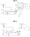
- Fig. 2 is a circuit diagram showing a main section related to a power-supply monitoring function of an inverter control device according to an embodiment of the present invention, corresponding to a part of Fig. 1 , consisting of microcontroller 21, insulation transformer power-supply circuit 22, insulation element 23, power-supply monitoring section 24 and low-voltage side battery 31.
- the input terminal of power-supply monitoring IC 3 is connected to the output terminal of low-voltage side battery 31 via diode 7 and resistance r D , and is grounded via resistance r E .
- the output terminal of power-supply monitoring IC 3 is connected to the output terminal of low-voltage side battery via diode 7 and resistance r A , and is also connected to the base terminal of transistor 4 via resistance r B .
- the emitter terminal of transistor 4 is grounded and is connected to the base terminal of transistor 4 via resistance r C .
- the collector terminal of transistor 4 is connected to the output terminal of low-voltage side sub power supply (LV5V power supply) 2 via light emitting diode 5 as a light emitting element of insulation element 23, while the ON/OFF of the collector current from low-voltage side sub power supply 2 switches ON/OFF the electric current flowing to phototransistor 6 as a light receiving element of insulation element 23.
- microcontroller 21 which is provided in high-voltage side circuit 37, the positive power input terminal is connected to the positive output terminal of insulation transformer power-supply circuit 22 and the negative power input terminal is connected to the collector terminal of phototransistor 6. Also, the positive power input terminal of microcontroller 21 is connected to the negative power input terminal of microcontroller 21 via resistance r G . Besides, the emitter terminal of phototransistor 6 is grounded.
- Such a circuit as shown in Fig. 2 makes it possible to utilize the input signal of microcontroller 21 via insulation element 23 as a signal which shows voltage reduction, because base current (I B ) and voltage (V BE ) between base and emitter become zero (which is because low-voltage side sub power supply 2 has been configured to hold the voltage while electricity is interrupted for a moment) when the output voltage of low-voltage side battery 31 instantly becomes zero.
- V ST V MOV ⁇ R D + R E / R E + V Fmax V ST - V Fmax ⁇ R C / R A + R B + R C ⁇ V BEmin
- V TH threshold voltage of power-supply monitoring IC
- V A output voltage of low-voltage side battery when input voltage of power-supply monitoring IC is equal to V TH
- I Bmin minimum value for base current of transistor
- I Cmax maximum value for collector current of transistor
- V BEmin minimum value for voltage between base and emitter of transistor
- V BEmax maximum value for voltage between base and emitter of transistor
- V MOV minimum operating voltage of power-supply monitoring IC
- V ST output voltage of low-voltage side battery when input voltage of power-supply monitoring IC is equal to V MOV
- R A electric resistance value of resistance r A
- R B electric resistance value of resistance r B
- R C electric resistance value of resistance r C
- R D electric resistance value of resistance r D
- R E electric resistance value of resistance r E
- the circuit is preferably configured, such that minimum values within error of electric resistance for R A ,R B ,R E satisfy relational Formulas 1 and 2 and that maximum values within error of electric resistance for R C ,R D satisfy relational Formulas 1 and 2. Further, the circuit is preferably configured, such that maximum values within error of electric resistance for R A ,R B satisfy relational Formula 4, that minimum values within error of electric resistance for R C ,V A satisfy relational Formula 4 and that minimum value within error of electric resistance for h FE satisfies relational Formula 5.
- Fig. 3 shows a main section related to a power-supply monitoring function of an inverter control device according to another embodiment of the present invention.
- Fig. 3 since basic principle and operation are the same as in Fig. 2 , explanations will be omitted by giving the same symbols to corresponding parts.
- Fig. 3 The difference between Fig. 3 and Fig. 2 is that insulation border 38, which exists in Fig.2 , does not exist in Fig. 3 . Since insulation border 38 does not exist, insulation transformer power-supply circuit 22 and insulation element 23 in Fig. 2 is not in Fig. 3 . Further, microcontroller 21 is supplied with electric power for control from low-voltage sub power supply in place of insulation transformer power-supply circuit 22 in Fig. 2 . Furthermore, resistance r F has been omitted.
- the input signal of microcontroller 21 can be utilized as a signal which shows voltage reduction when the output voltage of low-voltage side battery 31 instantly becomes zero, as in Fig. 2 .
- relational Formulas 1 - 5 referred to in the case of Fig. 2 can be used to design electrical resistance levels (R A ,R B ,R C ,R D ,R E ) of resistances (r A ,r B ,r C ,r D ,r E ).
- An inverter control device is applicable to various devices which is required to properly control against abnormal voltage reduction of a main power supply. Specifically, it is suitable for controlling electric compressor for vehicles, etc.
Landscapes
- Engineering & Computer Science (AREA)
- Power Engineering (AREA)
- Physics & Mathematics (AREA)
- General Physics & Mathematics (AREA)
- Inverter Devices (AREA)
- Control Of Ac Motors In General (AREA)
Applications Claiming Priority (2)
| Application Number | Priority Date | Filing Date | Title |
|---|---|---|---|
| JP2009130288A JP5317834B2 (ja) | 2009-05-29 | 2009-05-29 | インバータ制御装置 |
| PCT/JP2010/059146 WO2010137708A1 (ja) | 2009-05-29 | 2010-05-28 | インバータ制御装置 |
Publications (3)
| Publication Number | Publication Date |
|---|---|
| EP2437388A1 true EP2437388A1 (de) | 2012-04-04 |
| EP2437388A4 EP2437388A4 (de) | 2017-09-13 |
| EP2437388B1 EP2437388B1 (de) | 2019-12-04 |
Family
ID=43222811
Family Applications (1)
| Application Number | Title | Priority Date | Filing Date |
|---|---|---|---|
| EP10780662.2A Active EP2437388B1 (de) | 2009-05-29 | 2010-05-28 | Umrichtersteuerungsvorrichtung |
Country Status (5)
| Country | Link |
|---|---|
| US (1) | US8653776B2 (de) |
| EP (1) | EP2437388B1 (de) |
| JP (1) | JP5317834B2 (de) |
| CN (1) | CN102449899B (de) |
| WO (1) | WO2010137708A1 (de) |
Families Citing this family (8)
| Publication number | Priority date | Publication date | Assignee | Title |
|---|---|---|---|---|
| JP5567381B2 (ja) * | 2010-04-27 | 2014-08-06 | 日立オートモティブシステムズ株式会社 | 電力変換装置 |
| EP2600492B1 (de) * | 2011-12-01 | 2015-05-06 | AEG Power Solutions GmbH | Anordnung zur unterbrechungsfreien Stromversorgung |
| JP5755933B2 (ja) * | 2011-05-12 | 2015-07-29 | 東洋電機製造株式会社 | 電流極性判別器付きスイッチ |
| JP6638504B2 (ja) * | 2016-03-22 | 2020-01-29 | アイシン・エィ・ダブリュ株式会社 | インバータ駆動装置 |
| JP6961535B2 (ja) * | 2018-06-06 | 2021-11-05 | 三菱重工サーマルシステムズ株式会社 | 車載空調機制御装置及び車両 |
| CN110597140A (zh) * | 2019-09-26 | 2019-12-20 | 深圳博用科技有限公司 | 一种通过pwm信号反馈车用电机与控制器状态技术 |
| CN116722758B (zh) * | 2023-08-10 | 2023-12-29 | 深圳市智赋新能源有限公司 | 一种微型逆变器控制系统 |
| CN120320396A (zh) * | 2024-01-15 | 2025-07-15 | 中兴通讯股份有限公司 | 逆变器供电系统控制方法及逆变器、存储介质、程序产品 |
Family Cites Families (10)
| Publication number | Priority date | Publication date | Assignee | Title |
|---|---|---|---|---|
| JPH06121404A (ja) * | 1992-10-06 | 1994-04-28 | Hitachi Ltd | 電気車の制御装置 |
| JPH0772185A (ja) | 1993-09-02 | 1995-03-17 | Fujitsu Ten Ltd | 電源電圧監視回路 |
| JPH08266087A (ja) * | 1995-03-27 | 1996-10-11 | Nippondenso Co Ltd | インバータ装置 |
| JPH1014098A (ja) * | 1996-06-21 | 1998-01-16 | Daikin Ind Ltd | 電動機の駆動制御装置 |
| US5959851A (en) * | 1996-09-13 | 1999-09-28 | Thomson Consumer Electronics, Inc. | Switched-mode power supply control circuit |
| JP4037380B2 (ja) * | 2004-03-30 | 2008-01-23 | 三菱電機株式会社 | 電圧補償装置 |
| US7813096B2 (en) * | 2005-12-26 | 2010-10-12 | Autonetworks Technologies, Ltd. | Power supply controller |
| JP2008312342A (ja) * | 2007-06-14 | 2008-12-25 | Sanden Corp | 電動圧縮機の制御装置 |
| JP5164806B2 (ja) * | 2008-11-12 | 2013-03-21 | サンデン株式会社 | 車両用通信制御装置 |
| JP5242367B2 (ja) * | 2008-12-24 | 2013-07-24 | セイコーインスツル株式会社 | 基準電圧回路 |
-
2009
- 2009-05-29 JP JP2009130288A patent/JP5317834B2/ja active Active
-
2010
- 2010-05-28 EP EP10780662.2A patent/EP2437388B1/de active Active
- 2010-05-28 US US13/375,201 patent/US8653776B2/en active Active
- 2010-05-28 WO PCT/JP2010/059146 patent/WO2010137708A1/ja not_active Ceased
- 2010-05-28 CN CN201080024656.7A patent/CN102449899B/zh active Active
Non-Patent Citations (1)
| Title |
|---|
| See references of WO2010137708A1 * |
Also Published As
| Publication number | Publication date |
|---|---|
| WO2010137708A1 (ja) | 2010-12-02 |
| EP2437388A4 (de) | 2017-09-13 |
| US8653776B2 (en) | 2014-02-18 |
| CN102449899A (zh) | 2012-05-09 |
| CN102449899B (zh) | 2014-06-11 |
| US20120074889A1 (en) | 2012-03-29 |
| JP5317834B2 (ja) | 2013-10-16 |
| EP2437388B1 (de) | 2019-12-04 |
| JP2010279195A (ja) | 2010-12-09 |
Similar Documents
| Publication | Publication Date | Title |
|---|---|---|
| EP2437388B1 (de) | Umrichtersteuerungsvorrichtung | |
| US8891210B2 (en) | Electronic control unit including discharging circuit with plurality of resistors connected in series | |
| US11888388B2 (en) | Electric compressor control device | |
| JP4621231B2 (ja) | 電源保護装置及び電子制御装置 | |
| CN110266245B (zh) | 电机驱动系统、方法、电机驱动器及电动汽车 | |
| CN108767808B (zh) | 一种eps控制器电源诊断与保护系统及方法 | |
| JP4158112B2 (ja) | 車両用突入電流制限型電源スイッチ回路 | |
| CN112216558A (zh) | 继电器驱动电路和电气系统 | |
| CN110884558B (zh) | 用于向车辆中的eps供应电力的控制装置和方法 | |
| CN111284345A (zh) | 车辆的隔离充电控制设备及系统 | |
| CN215728550U (zh) | 一种继电器线圈短路与开路的诊断电路 | |
| US10879891B2 (en) | Power supply voltage monitoring circuit and control device | |
| US20130062936A1 (en) | Load control device | |
| CN1744423B (zh) | 功率半导体装置的控制用电路及控制用集成电路 | |
| CN223533351U (zh) | 一种高压互锁检测系统和车辆 | |
| CN112510810B (zh) | 一种汽车及其电源系统的监控电路 | |
| CN211180103U (zh) | 高压继电器的诊断装置及系统 | |
| CN103010291A (zh) | 车速信号采集装置及电动助力转向系统 | |
| CN216300786U (zh) | 电机控制器的放电电路 | |
| CN222884328U (zh) | 一种用于工业车辆电动转向助力系统的母线过欠压保护电路 | |
| CN111231704B (zh) | 非接触式供电系统 | |
| JP2015186303A (ja) | 回転電機制御装置 | |
| JP2019187042A (ja) | 平滑コンデンサの放電方法及び放電装置 | |
| KR101606234B1 (ko) | 전동식 조향장치 및 그의 단락검출방법 | |
| CN211830732U (zh) | 电机控制器的驱动电路以及具有其的车辆 |
Legal Events
| Date | Code | Title | Description |
|---|---|---|---|
| PUAI | Public reference made under article 153(3) epc to a published international application that has entered the european phase |
Free format text: ORIGINAL CODE: 0009012 |
|
| 17P | Request for examination filed |
Effective date: 20111227 |
|
| AK | Designated contracting states |
Kind code of ref document: A1 Designated state(s): AL AT BE BG CH CY CZ DE DK EE ES FI FR GB GR HR HU IE IS IT LI LT LU LV MC MK MT NL NO PL PT RO SE SI SK SM TR |
|
| DAX | Request for extension of the european patent (deleted) | ||
| RAP1 | Party data changed (applicant data changed or rights of an application transferred) |
Owner name: SANDEN HOLDINGS CORPORATION |
|
| REG | Reference to a national code |
Ref country code: DE Ref legal event code: R079 Ref document number: 602010062260 Country of ref document: DE Free format text: PREVIOUS MAIN CLASS: H02M0007480000 Ipc: H02M0001320000 |
|
| RA4 | Supplementary search report drawn up and despatched (corrected) |
Effective date: 20170816 |
|
| RIC1 | Information provided on ipc code assigned before grant |
Ipc: H02M 1/00 20070101ALI20170809BHEP Ipc: H03K 17/687 20060101ALI20170809BHEP Ipc: H03K 17/605 20060101ALI20170809BHEP Ipc: G01R 19/165 20060101ALI20170809BHEP Ipc: H02M 3/335 20060101ALI20170809BHEP Ipc: H03K 17/22 20060101ALI20170809BHEP Ipc: H02M 1/32 20070101AFI20170809BHEP |
|
| RIN1 | Information on inventor provided before grant (corrected) |
Inventor name: KUROSAKI, KEI |
|
| STAA | Information on the status of an ep patent application or granted ep patent |
Free format text: STATUS: EXAMINATION IS IN PROGRESS |
|
| 17Q | First examination report despatched |
Effective date: 20180713 |
|
| GRAP | Despatch of communication of intention to grant a patent |
Free format text: ORIGINAL CODE: EPIDOSNIGR1 |
|
| STAA | Information on the status of an ep patent application or granted ep patent |
Free format text: STATUS: GRANT OF PATENT IS INTENDED |
|
| INTG | Intention to grant announced |
Effective date: 20190401 |
|
| GRAJ | Information related to disapproval of communication of intention to grant by the applicant or resumption of examination proceedings by the epo deleted |
Free format text: ORIGINAL CODE: EPIDOSDIGR1 |
|
| STAA | Information on the status of an ep patent application or granted ep patent |
Free format text: STATUS: EXAMINATION IS IN PROGRESS |
|
| GRAP | Despatch of communication of intention to grant a patent |
Free format text: ORIGINAL CODE: EPIDOSNIGR1 |
|
| STAA | Information on the status of an ep patent application or granted ep patent |
Free format text: STATUS: GRANT OF PATENT IS INTENDED |
|
| INTC | Intention to grant announced (deleted) | ||
| INTG | Intention to grant announced |
Effective date: 20190807 |
|
| GRAS | Grant fee paid |
Free format text: ORIGINAL CODE: EPIDOSNIGR3 |
|
| GRAA | (expected) grant |
Free format text: ORIGINAL CODE: 0009210 |
|
| STAA | Information on the status of an ep patent application or granted ep patent |
Free format text: STATUS: THE PATENT HAS BEEN GRANTED |
|
| AK | Designated contracting states |
Kind code of ref document: B1 Designated state(s): AL AT BE BG CH CY CZ DE DK EE ES FI FR GB GR HR HU IE IS IT LI LT LU LV MC MK MT NL NO PL PT RO SE SI SK SM TR |
|
| REG | Reference to a national code |
Ref country code: GB Ref legal event code: FG4D |
|
| REG | Reference to a national code |
Ref country code: CH Ref legal event code: EP |
|
| REG | Reference to a national code |
Ref country code: AT Ref legal event code: REF Ref document number: 1210672 Country of ref document: AT Kind code of ref document: T Effective date: 20191215 |
|
| REG | Reference to a national code |
Ref country code: DE Ref legal event code: R096 Ref document number: 602010062260 Country of ref document: DE |
|
| REG | Reference to a national code |
Ref country code: IE Ref legal event code: FG4D |
|
| REG | Reference to a national code |
Ref country code: NL Ref legal event code: MP Effective date: 20191204 |
|
| REG | Reference to a national code |
Ref country code: LT Ref legal event code: MG4D |
|
| PG25 | Lapsed in a contracting state [announced via postgrant information from national office to epo] |
Ref country code: FI Free format text: LAPSE BECAUSE OF FAILURE TO SUBMIT A TRANSLATION OF THE DESCRIPTION OR TO PAY THE FEE WITHIN THE PRESCRIBED TIME-LIMIT Effective date: 20191204 Ref country code: BG Free format text: LAPSE BECAUSE OF FAILURE TO SUBMIT A TRANSLATION OF THE DESCRIPTION OR TO PAY THE FEE WITHIN THE PRESCRIBED TIME-LIMIT Effective date: 20200304 Ref country code: LT Free format text: LAPSE BECAUSE OF FAILURE TO SUBMIT A TRANSLATION OF THE DESCRIPTION OR TO PAY THE FEE WITHIN THE PRESCRIBED TIME-LIMIT Effective date: 20191204 Ref country code: ES Free format text: LAPSE BECAUSE OF FAILURE TO SUBMIT A TRANSLATION OF THE DESCRIPTION OR TO PAY THE FEE WITHIN THE PRESCRIBED TIME-LIMIT Effective date: 20191204 Ref country code: GR Free format text: LAPSE BECAUSE OF FAILURE TO SUBMIT A TRANSLATION OF THE DESCRIPTION OR TO PAY THE FEE WITHIN THE PRESCRIBED TIME-LIMIT Effective date: 20200305 Ref country code: NO Free format text: LAPSE BECAUSE OF FAILURE TO SUBMIT A TRANSLATION OF THE DESCRIPTION OR TO PAY THE FEE WITHIN THE PRESCRIBED TIME-LIMIT Effective date: 20200304 Ref country code: SE Free format text: LAPSE BECAUSE OF FAILURE TO SUBMIT A TRANSLATION OF THE DESCRIPTION OR TO PAY THE FEE WITHIN THE PRESCRIBED TIME-LIMIT Effective date: 20191204 Ref country code: LV Free format text: LAPSE BECAUSE OF FAILURE TO SUBMIT A TRANSLATION OF THE DESCRIPTION OR TO PAY THE FEE WITHIN THE PRESCRIBED TIME-LIMIT Effective date: 20191204 |
|
| PG25 | Lapsed in a contracting state [announced via postgrant information from national office to epo] |
Ref country code: HR Free format text: LAPSE BECAUSE OF FAILURE TO SUBMIT A TRANSLATION OF THE DESCRIPTION OR TO PAY THE FEE WITHIN THE PRESCRIBED TIME-LIMIT Effective date: 20191204 |
|
| PG25 | Lapsed in a contracting state [announced via postgrant information from national office to epo] |
Ref country code: AL Free format text: LAPSE BECAUSE OF FAILURE TO SUBMIT A TRANSLATION OF THE DESCRIPTION OR TO PAY THE FEE WITHIN THE PRESCRIBED TIME-LIMIT Effective date: 20191204 |
|
| PG25 | Lapsed in a contracting state [announced via postgrant information from national office to epo] |
Ref country code: NL Free format text: LAPSE BECAUSE OF FAILURE TO SUBMIT A TRANSLATION OF THE DESCRIPTION OR TO PAY THE FEE WITHIN THE PRESCRIBED TIME-LIMIT Effective date: 20191204 Ref country code: RO Free format text: LAPSE BECAUSE OF FAILURE TO SUBMIT A TRANSLATION OF THE DESCRIPTION OR TO PAY THE FEE WITHIN THE PRESCRIBED TIME-LIMIT Effective date: 20191204 Ref country code: CZ Free format text: LAPSE BECAUSE OF FAILURE TO SUBMIT A TRANSLATION OF THE DESCRIPTION OR TO PAY THE FEE WITHIN THE PRESCRIBED TIME-LIMIT Effective date: 20191204 Ref country code: PT Free format text: LAPSE BECAUSE OF FAILURE TO SUBMIT A TRANSLATION OF THE DESCRIPTION OR TO PAY THE FEE WITHIN THE PRESCRIBED TIME-LIMIT Effective date: 20200429 Ref country code: EE Free format text: LAPSE BECAUSE OF FAILURE TO SUBMIT A TRANSLATION OF THE DESCRIPTION OR TO PAY THE FEE WITHIN THE PRESCRIBED TIME-LIMIT Effective date: 20191204 |
|
| PG25 | Lapsed in a contracting state [announced via postgrant information from national office to epo] |
Ref country code: SK Free format text: LAPSE BECAUSE OF FAILURE TO SUBMIT A TRANSLATION OF THE DESCRIPTION OR TO PAY THE FEE WITHIN THE PRESCRIBED TIME-LIMIT Effective date: 20191204 Ref country code: IS Free format text: LAPSE BECAUSE OF FAILURE TO SUBMIT A TRANSLATION OF THE DESCRIPTION OR TO PAY THE FEE WITHIN THE PRESCRIBED TIME-LIMIT Effective date: 20200404 Ref country code: SM Free format text: LAPSE BECAUSE OF FAILURE TO SUBMIT A TRANSLATION OF THE DESCRIPTION OR TO PAY THE FEE WITHIN THE PRESCRIBED TIME-LIMIT Effective date: 20191204 |
|
| REG | Reference to a national code |
Ref country code: DE Ref legal event code: R097 Ref document number: 602010062260 Country of ref document: DE |
|
| REG | Reference to a national code |
Ref country code: AT Ref legal event code: MK05 Ref document number: 1210672 Country of ref document: AT Kind code of ref document: T Effective date: 20191204 |
|
| PLBE | No opposition filed within time limit |
Free format text: ORIGINAL CODE: 0009261 |
|
| STAA | Information on the status of an ep patent application or granted ep patent |
Free format text: STATUS: NO OPPOSITION FILED WITHIN TIME LIMIT |
|
| PG25 | Lapsed in a contracting state [announced via postgrant information from national office to epo] |
Ref country code: DK Free format text: LAPSE BECAUSE OF FAILURE TO SUBMIT A TRANSLATION OF THE DESCRIPTION OR TO PAY THE FEE WITHIN THE PRESCRIBED TIME-LIMIT Effective date: 20191204 |
|
| 26N | No opposition filed |
Effective date: 20200907 |
|
| PG25 | Lapsed in a contracting state [announced via postgrant information from national office to epo] |
Ref country code: PL Free format text: LAPSE BECAUSE OF FAILURE TO SUBMIT A TRANSLATION OF THE DESCRIPTION OR TO PAY THE FEE WITHIN THE PRESCRIBED TIME-LIMIT Effective date: 20191204 Ref country code: SI Free format text: LAPSE BECAUSE OF FAILURE TO SUBMIT A TRANSLATION OF THE DESCRIPTION OR TO PAY THE FEE WITHIN THE PRESCRIBED TIME-LIMIT Effective date: 20191204 Ref country code: AT Free format text: LAPSE BECAUSE OF FAILURE TO SUBMIT A TRANSLATION OF THE DESCRIPTION OR TO PAY THE FEE WITHIN THE PRESCRIBED TIME-LIMIT Effective date: 20191204 |
|
| PG25 | Lapsed in a contracting state [announced via postgrant information from national office to epo] |
Ref country code: LI Free format text: LAPSE BECAUSE OF NON-PAYMENT OF DUE FEES Effective date: 20200531 Ref country code: MC Free format text: LAPSE BECAUSE OF FAILURE TO SUBMIT A TRANSLATION OF THE DESCRIPTION OR TO PAY THE FEE WITHIN THE PRESCRIBED TIME-LIMIT Effective date: 20191204 Ref country code: CH Free format text: LAPSE BECAUSE OF NON-PAYMENT OF DUE FEES Effective date: 20200531 Ref country code: IT Free format text: LAPSE BECAUSE OF FAILURE TO SUBMIT A TRANSLATION OF THE DESCRIPTION OR TO PAY THE FEE WITHIN THE PRESCRIBED TIME-LIMIT Effective date: 20191204 |
|
| REG | Reference to a national code |
Ref country code: BE Ref legal event code: MM Effective date: 20200531 |
|
| GBPC | Gb: european patent ceased through non-payment of renewal fee |
Effective date: 20200528 |
|
| PG25 | Lapsed in a contracting state [announced via postgrant information from national office to epo] |
Ref country code: LU Free format text: LAPSE BECAUSE OF NON-PAYMENT OF DUE FEES Effective date: 20200528 |
|
| PG25 | Lapsed in a contracting state [announced via postgrant information from national office to epo] |
Ref country code: FR Free format text: LAPSE BECAUSE OF NON-PAYMENT OF DUE FEES Effective date: 20200531 Ref country code: GB Free format text: LAPSE BECAUSE OF NON-PAYMENT OF DUE FEES Effective date: 20200528 Ref country code: IE Free format text: LAPSE BECAUSE OF NON-PAYMENT OF DUE FEES Effective date: 20200528 |
|
| PG25 | Lapsed in a contracting state [announced via postgrant information from national office to epo] |
Ref country code: BE Free format text: LAPSE BECAUSE OF NON-PAYMENT OF DUE FEES Effective date: 20200531 |
|
| PG25 | Lapsed in a contracting state [announced via postgrant information from national office to epo] |
Ref country code: TR Free format text: LAPSE BECAUSE OF FAILURE TO SUBMIT A TRANSLATION OF THE DESCRIPTION OR TO PAY THE FEE WITHIN THE PRESCRIBED TIME-LIMIT Effective date: 20191204 Ref country code: MT Free format text: LAPSE BECAUSE OF FAILURE TO SUBMIT A TRANSLATION OF THE DESCRIPTION OR TO PAY THE FEE WITHIN THE PRESCRIBED TIME-LIMIT Effective date: 20191204 Ref country code: CY Free format text: LAPSE BECAUSE OF FAILURE TO SUBMIT A TRANSLATION OF THE DESCRIPTION OR TO PAY THE FEE WITHIN THE PRESCRIBED TIME-LIMIT Effective date: 20191204 |
|
| PG25 | Lapsed in a contracting state [announced via postgrant information from national office to epo] |
Ref country code: MK Free format text: LAPSE BECAUSE OF FAILURE TO SUBMIT A TRANSLATION OF THE DESCRIPTION OR TO PAY THE FEE WITHIN THE PRESCRIBED TIME-LIMIT Effective date: 20191204 |
|
| REG | Reference to a national code |
Ref country code: DE Ref legal event code: R081 Ref document number: 602010062260 Country of ref document: DE Owner name: SANDEN CORPORATION, ISESAKI-SHI, JP Free format text: FORMER OWNER: SANDEN HOLDINGS CORPORATION, LSESAKI-SHI, GUNMA, JP |
|
| PGFP | Annual fee paid to national office [announced via postgrant information from national office to epo] |
Ref country code: DE Payment date: 20250423 Year of fee payment: 16 |