EP2442364A1 - Structure d'empilement de porte pour dispositif à mémoire flash à semi-conducteur et son procédé de préparation - Google Patents
Structure d'empilement de porte pour dispositif à mémoire flash à semi-conducteur et son procédé de préparation Download PDFInfo
- Publication number
- EP2442364A1 EP2442364A1 EP11789049A EP11789049A EP2442364A1 EP 2442364 A1 EP2442364 A1 EP 2442364A1 EP 11789049 A EP11789049 A EP 11789049A EP 11789049 A EP11789049 A EP 11789049A EP 2442364 A1 EP2442364 A1 EP 2442364A1
- Authority
- EP
- European Patent Office
- Prior art keywords
- film
- layer
- nanocrystals
- ald
- stack structure
- Prior art date
- Legal status (The legal status is an assumption and is not a legal conclusion. Google has not performed a legal analysis and makes no representation as to the accuracy of the status listed.)
- Withdrawn
Links
Images


Classifications
-
- C—CHEMISTRY; METALLURGY
- C23—COATING METALLIC MATERIAL; COATING MATERIAL WITH METALLIC MATERIAL; CHEMICAL SURFACE TREATMENT; DIFFUSION TREATMENT OF METALLIC MATERIAL; COATING BY VACUUM EVAPORATION, BY SPUTTERING, BY ION IMPLANTATION OR BY CHEMICAL VAPOUR DEPOSITION, IN GENERAL; INHIBITING CORROSION OF METALLIC MATERIAL OR INCRUSTATION IN GENERAL
- C23C—COATING METALLIC MATERIAL; COATING MATERIAL WITH METALLIC MATERIAL; SURFACE TREATMENT OF METALLIC MATERIAL BY DIFFUSION INTO THE SURFACE, BY CHEMICAL CONVERSION OR SUBSTITUTION; COATING BY VACUUM EVAPORATION, BY SPUTTERING, BY ION IMPLANTATION OR BY CHEMICAL VAPOUR DEPOSITION, IN GENERAL
- C23C16/00—Chemical coating by decomposition of gaseous compounds, without leaving reaction products of surface material in the coating, i.e. chemical vapour deposition [CVD] processes
- C23C16/44—Chemical coating by decomposition of gaseous compounds, without leaving reaction products of surface material in the coating, i.e. chemical vapour deposition [CVD] processes characterised by the method of coating
- C23C16/455—Chemical coating by decomposition of gaseous compounds, without leaving reaction products of surface material in the coating, i.e. chemical vapour deposition [CVD] processes characterised by the method of coating characterised by the method used for introducing gases into reaction chamber or for modifying gas flows in reaction chamber
- C23C16/45523—Pulsed gas flow or change of composition over time
- C23C16/45525—Atomic layer deposition [ALD]
-
- B—PERFORMING OPERATIONS; TRANSPORTING
- B82—NANOTECHNOLOGY
- B82Y—SPECIFIC USES OR APPLICATIONS OF NANOSTRUCTURES; MEASUREMENT OR ANALYSIS OF NANOSTRUCTURES; MANUFACTURE OR TREATMENT OF NANOSTRUCTURES
- B82Y10/00—Nanotechnology for information processing, storage or transmission, e.g. quantum computing or single electron logic
-
- C—CHEMISTRY; METALLURGY
- C23—COATING METALLIC MATERIAL; COATING MATERIAL WITH METALLIC MATERIAL; CHEMICAL SURFACE TREATMENT; DIFFUSION TREATMENT OF METALLIC MATERIAL; COATING BY VACUUM EVAPORATION, BY SPUTTERING, BY ION IMPLANTATION OR BY CHEMICAL VAPOUR DEPOSITION, IN GENERAL; INHIBITING CORROSION OF METALLIC MATERIAL OR INCRUSTATION IN GENERAL
- C23C—COATING METALLIC MATERIAL; COATING MATERIAL WITH METALLIC MATERIAL; SURFACE TREATMENT OF METALLIC MATERIAL BY DIFFUSION INTO THE SURFACE, BY CHEMICAL CONVERSION OR SUBSTITUTION; COATING BY VACUUM EVAPORATION, BY SPUTTERING, BY ION IMPLANTATION OR BY CHEMICAL VAPOUR DEPOSITION, IN GENERAL
- C23C16/00—Chemical coating by decomposition of gaseous compounds, without leaving reaction products of surface material in the coating, i.e. chemical vapour deposition [CVD] processes
- C23C16/22—Chemical coating by decomposition of gaseous compounds, without leaving reaction products of surface material in the coating, i.e. chemical vapour deposition [CVD] processes characterised by the deposition of inorganic material, other than metallic material
- C23C16/30—Deposition of compounds, mixtures or solid solutions, e.g. borides, carbides, nitrides
- C23C16/40—Oxides
-
- H—ELECTRICITY
- H10—SEMICONDUCTOR DEVICES; ELECTRIC SOLID-STATE DEVICES NOT OTHERWISE PROVIDED FOR
- H10D—INORGANIC ELECTRIC SEMICONDUCTOR DEVICES
- H10D30/00—Field-effect transistors [FET]
- H10D30/60—Insulated-gate field-effect transistors [IGFET]
- H10D30/68—Floating-gate IGFETs
- H10D30/6891—Floating-gate IGFETs characterised by the shapes, relative sizes or dispositions of the floating gate electrode
- H10D30/6893—Floating-gate IGFETs characterised by the shapes, relative sizes or dispositions of the floating gate electrode wherein the floating gate has multiple non-connected parts, e.g. multi-particle floating gate
-
- H—ELECTRICITY
- H10—SEMICONDUCTOR DEVICES; ELECTRIC SOLID-STATE DEVICES NOT OTHERWISE PROVIDED FOR
- H10D—INORGANIC ELECTRIC SEMICONDUCTOR DEVICES
- H10D30/00—Field-effect transistors [FET]
- H10D30/60—Insulated-gate field-effect transistors [IGFET]
- H10D30/69—IGFETs having charge trapping gate insulators, e.g. MNOS transistors
- H10D30/694—IGFETs having charge trapping gate insulators, e.g. MNOS transistors characterised by the shapes, relative sizes or dispositions of the gate electrodes
-
- H—ELECTRICITY
- H10—SEMICONDUCTOR DEVICES; ELECTRIC SOLID-STATE DEVICES NOT OTHERWISE PROVIDED FOR
- H10D—INORGANIC ELECTRIC SEMICONDUCTOR DEVICES
- H10D64/00—Electrodes of devices having potential barriers
- H10D64/01—Manufacture or treatment
- H10D64/013—Manufacture or treatment of electrodes having a conductor capacitively coupled to a semiconductor by an insulator
- H10D64/01302—Manufacture or treatment of electrodes having a conductor capacitively coupled to a semiconductor by an insulator the insulator being formed after the semiconductor body, the semiconductor being silicon
- H10D64/01304—Manufacture or treatment of electrodes having a conductor capacitively coupled to a semiconductor by an insulator the insulator being formed after the semiconductor body, the semiconductor being silicon characterised by the conductor
- H10D64/01316—Manufacture or treatment of electrodes having a conductor capacitively coupled to a semiconductor by an insulator the insulator being formed after the semiconductor body, the semiconductor being silicon characterised by the conductor the conductor comprising a layer of elemental metal contacting the insulator, e.g. Ta, W, Mo or Al
-
- H—ELECTRICITY
- H10—SEMICONDUCTOR DEVICES; ELECTRIC SOLID-STATE DEVICES NOT OTHERWISE PROVIDED FOR
- H10D—INORGANIC ELECTRIC SEMICONDUCTOR DEVICES
- H10D64/00—Electrodes of devices having potential barriers
- H10D64/01—Manufacture or treatment
- H10D64/031—Manufacture or treatment of data-storage electrodes
- H10D64/035—Manufacture or treatment of data-storage electrodes comprising conductor-insulator-conductor-insulator-semiconductor structures
-
- H—ELECTRICITY
- H10—SEMICONDUCTOR DEVICES; ELECTRIC SOLID-STATE DEVICES NOT OTHERWISE PROVIDED FOR
- H10D—INORGANIC ELECTRIC SEMICONDUCTOR DEVICES
- H10D64/00—Electrodes of devices having potential barriers
- H10D64/01—Manufacture or treatment
- H10D64/031—Manufacture or treatment of data-storage electrodes
- H10D64/037—Manufacture or treatment of data-storage electrodes comprising charge-trapping insulators
-
- H—ELECTRICITY
- H10—SEMICONDUCTOR DEVICES; ELECTRIC SOLID-STATE DEVICES NOT OTHERWISE PROVIDED FOR
- H10D—INORGANIC ELECTRIC SEMICONDUCTOR DEVICES
- H10D64/00—Electrodes of devices having potential barriers
- H10D64/60—Electrodes characterised by their materials
- H10D64/66—Electrodes having a conductor capacitively coupled to a semiconductor by an insulator, e.g. MIS electrodes
- H10D64/665—Electrodes having a conductor capacitively coupled to a semiconductor by an insulator, e.g. MIS electrodes the conductor comprising a layer of elemental metal contacting the insulator, e.g. tungsten or molybdenum
Definitions
- the present invention relates to the fabrication of semiconductor integrated circuits, and, particularly to an electric capacity structure and a fabricating method of a flash memory capacitor. More specifically, it relates to a gate stack structure and a fabricating method with a novel heterogenous charge storage layer composed of metal nanocrystals and high permittivity (high-k) dielectric .
- nonvolatile memory based on discrete-charge storage nodes (such as nanocrystal memory and SONOS-type memory etc) has drawn great attention.
- the aforementioned memory devices use discrete charge traps to store charges in place of continuous poly-silicon floating gate, which can prevent a loss of massive charges stored in the charge-trapping layer through local defects in the tunnel layer, thus efficiently enhancing the data retention of memory, and achieving lower operating voltage and higher programming/erasing speed.
- metal nanocrystals Compared with semiconductor nanocrystals, metal nanocrystals have some advantages such as higher density of states around Fermi level, a wider range of work functions, stronger coupling with substrate channel and so on. Accordingly, the above mentioned advantages can ensure that the memory device has lower operating voltage, higher stored charge density and longer charge retention. Some research indicates that a deep potential well can be formed by using high work-function metal nanocrystals, thus efficiently trapping charges and offering better data retention.
- the object of the present invention is to provide a gate stack structure for use in a semiconductor flash memory device, which has a high stored-charge density, a low operating voltage, fast programing and erasing speeds, as well as good charge retention.
- the other object of the present invention is to offer a method of fabricating the above-mentioned gate stack structure.
- the present invention provides a gate stack structure for use in a semiconductor flash memory device and its fabricating method.
- the said gate stack structure contains a heterogeneous charge storage layer based on metal nanocrystals and high-k film.
- the aforementioned gate stack structure includes the following components in sequence from bottom to up:
- the above-mentioned high-k film can be HfAlO, as an example, it may consist of HfO 2 and Al 2 O 3 with a deposition cycle ratio of 1:1; Alternatively, said high-k film can be an HfO 2 film.
- the aforementioned top electrode layer contains a gate electrode which is composed of metal palladium (Pd).
- the fabricating method of the aforementioned gate stack structure includes the following steps:
- the high-k Hf x Al y O z film described in Step 3.2 can be HfAlO, which consists of HfO 2 and Al 2 O 3 with a deposition cycle ratio of 1:1.
- the said high-k Hf x Al y O z film can be HfO 2 .
- the experimental conditions for ALD (atomic layer deposition) of HfO 2 film are as follows: the substrate temperature is kept at 250 ⁇ 350°C, and the reaction precursors include tetrakis(ethylmethylamino)-hafnium (TEMAH) and water vapor.
- TEMAH tetrakis(ethylmethylamino)-hafnium
- step 3.2 and Step 4 the experimental conditions for ALD of Al 2 O 3 film are as follows: the substrate temperature is kept at 250 ⁇ 350°C, and the reaction precursors include trimethylaluminium (TMA) and water vapor.
- TMA trimethylaluminium
- the annealing temperature for the formation of RuO x nanocrystals is 700 ⁇ 900°C, and the annealing time is 10-30s.
- said rapid thermal annealing is carried out at 500 ⁇ 800°C for 10-30s during the formation of the Al 2 O 3 charge blocking layer.
- the gate electrode material is a metal of Pd.
- the aforementioned fabricating method also includes:
- the gate stack structure provided by the present invention will be very promising for next generation flash memory devices.
- the present invention relates to a gate stack structure for use in a semiconductor flash memory device, in particular, the related gate stack structure contains a heterogeneous charge storage layer consisting of metal nanocrystals and high-k film.
- Said flash memory capacitor includes the following components in sequence from bottom to top:
- Hf x Al y O z film is composed of HfO 2 and Al 2 O 3 with a deposition cycle ratio of 1:1, denoted by HfAlO.
- HfAlO a deposition cycle ratio of 1:1
- the temperature of the substrate is kept at a range of 250 ⁇ 350°C, and the precursors for HfO 2 include Tetrakis (ethylmethylamino) Hafnium (TEMAH) and water vapor.
- TEMAH Tetrakis (ethylmethylamino) Hafnium
- Al 2 O3 is as described in Step 2.
- HfAlO or HfO 2 film is controlled in a range of 3 ⁇ 20 nm (preferred thickness is 5 ⁇ 10 nm). Based on the difference of Hf x Al y O z film thickness, it is found that the Hf x Al y O z film can be present between nanocrystals when it is thin, but it cannot completely fill the gap between the nanocrystals. Otherwise, it can fill the gap between the nanocrystals completely when it is thick, as shown in Fig. 1 .
- Fig. 2 shows the flat-band voltages resulting from programming and erasing of the fabricated memory capacitors with different heterogeneous charge storage layer under different voltages for 0.1ms, respectively, .
- the programming voltage positive bias
- the resulting flat-band voltage shifts gradually towards a positive bias, and this is due to negative charge trapping caused by electron injection.
- the erasing voltage negative bias
- the resulting flat-band voltage moves gradually in the direction of negative bias, which is attributed to de-trapping of the negative charges stored in the charge storage layer or injection of holes from the substrate.
- the heterogeneous charge storage layer of RuO x /HfO 2 can provide a larger memory window than RuO x /HfAlO in the case of identical operating voltages.
- the former can result in a memory window of 2.6V, and the latter can lead to a memory window of 1.4V in the case of a 6V operating voltage.
- FIG. 3 shows the resulting flat-band voltages after programming under +9V and erasing under -9V of the fabricated memory capacitors with different heterogeneous charge storage layer for different times. It is seen that the resulting flat-band voltage increases with time under programming and erasing modes and finally tends to saturation. Regarding 0.1ms programming/erasing time, a memory window of around 2V was achieved for the RuO x /HfAlO charge storage layer-based capacitor, and a memory window of 3.5V was obtained for the RuO x /HfO 2 charge storage layer-based capacitor. Therefore, both of the capacitors exhibit fast programming and erasing characteristics under low operating voltages.
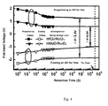
- Fig. 4 shows the retention characteristics of the fabricated memory capacitors with the heterogeneous charge storage layer-based gate stack structure after programming at +9V for 1ms and erasing at -9V for 1ms, respectively.
- the resulting memory window is close to 3.4V after ten years by extrapolation, thus exhibiting excellent charge retention.
- the charge trapping dielectric of HfAlO the corresponding memory window is around 1.6V.
- the present invention combines the advantages of both metal nanocrystals and high-k dielectrics, which act as the heterogeneous charge storage layer in the gate stack structure.
- the utilization of this kind of heterogeneous charge storage layer containing high-k dielectrics enhances the electric field across the charge tunnel layer, thus leading to a decrease in the potential barrier for charge injection, an increase in programming and erasing speeds and achievement of low operating voltages.
- the metal nanocrystals with a high work function can result in the formation of a deeper potential well, which can ensure good charge retention after charges trapping.
- the metal nanocrystals in the present invention are composed of Ru and Ru oxide (denoted by RuO x nanocrystals), which have excellent thermal stability. Though Ru is oxidized, it is still a good conductor. In addition, it does not diffuse easily at high temperature, and it is easy for dry etching.
- the top electrode of Pd in the present invention has a high work function of 5.22eV, and thus it combines with the charge blocking layer, resulting in a potential barrier propitious to programming and erasing.
- Pd has good chemical and thermal stabilities.
- the gate stack structure provided by the present invention will be very promising for next generation flash memory devices.
Landscapes
- Chemical & Material Sciences (AREA)
- Engineering & Computer Science (AREA)
- Nanotechnology (AREA)
- General Chemical & Material Sciences (AREA)
- Materials Engineering (AREA)
- Mechanical Engineering (AREA)
- Metallurgy (AREA)
- Organic Chemistry (AREA)
- Chemical Kinetics & Catalysis (AREA)
- Mathematical Physics (AREA)
- Theoretical Computer Science (AREA)
- Crystallography & Structural Chemistry (AREA)
- Physics & Mathematics (AREA)
- Inorganic Chemistry (AREA)
- Semiconductor Memories (AREA)
- Non-Volatile Memory (AREA)
Applications Claiming Priority (3)
| Application Number | Priority Date | Filing Date | Title |
|---|---|---|---|
| CN2010101916591A CN101887910A (zh) | 2010-06-03 | 2010-06-03 | 一种适合于半导体闪存器件的栅叠层结构及制备方法 |
| CN2011101304848A CN102208442B (zh) | 2010-06-03 | 2011-05-19 | 一种适合于半导体闪存器件的栅叠层结构及制备方法 |
| PCT/CN2011/000891 WO2011150670A1 (fr) | 2010-06-03 | 2011-05-24 | Structure d'empilement de porte pour dispositif à mémoire flash à semi-conducteur et son procédé de préparation |
Publications (2)
| Publication Number | Publication Date |
|---|---|
| EP2442364A1 true EP2442364A1 (fr) | 2012-04-18 |
| EP2442364A4 EP2442364A4 (fr) | 2014-08-27 |
Family
ID=43073727
Family Applications (1)
| Application Number | Title | Priority Date | Filing Date |
|---|---|---|---|
| EP11789049.1A Withdrawn EP2442364A4 (fr) | 2010-06-03 | 2011-05-24 | Structure d'empilement de porte pour dispositif à mémoire flash à semi-conducteur et son procédé de préparation |
Country Status (4)
| Country | Link |
|---|---|
| US (1) | US20130062684A1 (fr) |
| EP (1) | EP2442364A4 (fr) |
| CN (2) | CN101887910A (fr) |
| WO (1) | WO2011150670A1 (fr) |
Cited By (2)
| Publication number | Priority date | Publication date | Assignee | Title |
|---|---|---|---|---|
| WO2014113655A3 (fr) * | 2013-01-18 | 2014-10-16 | The Trustees Of The University Of Pennsylvania | Procédés et appareil de fabrication de dispositif en couches minces à nanocristaux |
| US9336919B2 (en) | 2012-08-17 | 2016-05-10 | The Trustees Of The University Of Pennsylvania | Methods for preparing colloidal nanocrystal-based thin films |
Families Citing this family (14)
| Publication number | Priority date | Publication date | Assignee | Title |
|---|---|---|---|---|
| CN101887910A (zh) * | 2010-06-03 | 2010-11-17 | 复旦大学 | 一种适合于半导体闪存器件的栅叠层结构及制备方法 |
| CN102646579B (zh) * | 2011-02-17 | 2015-01-07 | 中芯国际集成电路制造(上海)有限公司 | 一种sonos结构及制造方法 |
| CN102938404A (zh) * | 2011-08-16 | 2013-02-20 | 北京天中磊智能科技有限公司 | 一种智能电能表专用eeprom存储芯片 |
| CN102623459B (zh) * | 2012-04-10 | 2015-01-07 | 复旦大学 | 一种薄膜晶体管存储器及其制备方法 |
| WO2017044127A1 (fr) * | 2015-09-11 | 2017-03-16 | Intel Corporation | Transistor à tension de seuil dynamique pour veille avec faible fuite et mode actif à grande vitesse |
| KR102331474B1 (ko) | 2017-06-19 | 2021-11-29 | 삼성전자주식회사 | 반도체 장치 |
| JP2019062170A (ja) * | 2017-09-28 | 2019-04-18 | ルネサスエレクトロニクス株式会社 | 半導体装置およびその製造方法 |
| CN108649031A (zh) * | 2018-04-09 | 2018-10-12 | 复旦大学 | 基于自整流特性材料的二维超快准非易失存储器及其制备方法 |
| CN108588677B (zh) * | 2018-04-18 | 2020-09-08 | 北京航空航天大学 | 一种高介电常数的纳米叠层介电薄膜及其制备方法 |
| TWI815891B (zh) * | 2018-06-21 | 2023-09-21 | 美商應用材料股份有限公司 | 薄膜及沉積薄膜的方法 |
| CN109116691B (zh) * | 2018-09-25 | 2022-08-16 | 湖南哲龙科技有限公司 | 一种弱化基材表面对有机感光鼓特性影响的配方 |
| CN112080732B (zh) * | 2020-07-29 | 2021-12-28 | 西安交通大学 | 一种硅集成的bt-bmz薄膜、电容器及其制造方法 |
| CN112908999A (zh) * | 2021-03-25 | 2021-06-04 | 复旦大学 | 半浮栅存储器的制造工艺及半浮栅存储器 |
| US12356624B2 (en) * | 2021-08-30 | 2025-07-08 | Renesas Electronics Corporation | Semiconductor device and method of manufacturing the same |
Family Cites Families (7)
| Publication number | Priority date | Publication date | Assignee | Title |
|---|---|---|---|---|
| US7012297B2 (en) * | 2001-08-30 | 2006-03-14 | Micron Technology, Inc. | Scalable flash/NV structures and devices with extended endurance |
| KR100672998B1 (ko) * | 2005-02-14 | 2007-01-24 | 삼성전자주식회사 | 불휘발성 메모리 소자, 그 구동 방법 및 형성 방법 |
| US7629641B2 (en) * | 2005-08-31 | 2009-12-08 | Micron Technology, Inc. | Band engineered nano-crystal non-volatile memory device utilizing enhanced gate injection |
| US7847341B2 (en) * | 2006-12-20 | 2010-12-07 | Nanosys, Inc. | Electron blocking layers for electronic devices |
| KR100900569B1 (ko) * | 2007-03-29 | 2009-06-02 | 국민대학교산학협력단 | 플로팅 게이트 형성 방법 및 이를 이용한 비휘발성 메모리 장치의 제조 방법 |
| CN101692463B (zh) * | 2009-09-24 | 2011-12-14 | 复旦大学 | 一种混合纳米晶存储器的电容结构及其制备方法 |
| CN101887910A (zh) * | 2010-06-03 | 2010-11-17 | 复旦大学 | 一种适合于半导体闪存器件的栅叠层结构及制备方法 |
-
2010
- 2010-06-03 CN CN2010101916591A patent/CN101887910A/zh active Pending
-
2011
- 2011-05-19 CN CN2011101304848A patent/CN102208442B/zh not_active Expired - Fee Related
- 2011-05-24 WO PCT/CN2011/000891 patent/WO2011150670A1/fr not_active Ceased
- 2011-05-24 EP EP11789049.1A patent/EP2442364A4/fr not_active Withdrawn
- 2011-05-24 US US13/518,306 patent/US20130062684A1/en not_active Abandoned
Cited By (5)
| Publication number | Priority date | Publication date | Assignee | Title |
|---|---|---|---|---|
| US9336919B2 (en) | 2012-08-17 | 2016-05-10 | The Trustees Of The University Of Pennsylvania | Methods for preparing colloidal nanocrystal-based thin films |
| US10096734B2 (en) | 2012-08-17 | 2018-10-09 | The Trustees Of The University Of Pennsylvania | Methods of forming colloidal nanocrystal-based thin film devices |
| US10096733B2 (en) | 2012-08-17 | 2018-10-09 | The Trustees Of The University Of Pennsylvania | Methods for the preparation of colloidal nanocrystal dispersion |
| WO2014113655A3 (fr) * | 2013-01-18 | 2014-10-16 | The Trustees Of The University Of Pennsylvania | Procédés et appareil de fabrication de dispositif en couches minces à nanocristaux |
| US9865465B2 (en) | 2013-01-18 | 2018-01-09 | The Trustees Of The University Of Pennsylvania | Nanocrystal thin film fabrication methods and apparatus |
Also Published As
| Publication number | Publication date |
|---|---|
| EP2442364A4 (fr) | 2014-08-27 |
| CN101887910A (zh) | 2010-11-17 |
| WO2011150670A1 (fr) | 2011-12-08 |
| CN102208442A (zh) | 2011-10-05 |
| CN102208442B (zh) | 2013-04-17 |
| US20130062684A1 (en) | 2013-03-14 |
Similar Documents
| Publication | Publication Date | Title |
|---|---|---|
| EP2442364A1 (fr) | Structure d'empilement de porte pour dispositif à mémoire flash à semi-conducteur et son procédé de préparation | |
| US10211223B2 (en) | Vertical ferroelectric memory device and a method for manufacturing thereof | |
| US7183186B2 (en) | Atomic layer deposited ZrTiO4 films | |
| US20080023744A1 (en) | Nonvolatile semiconductor memory device and method of manufacturing the same | |
| KR20080031594A (ko) | 전하 트랩형 메모리 소자 | |
| US7579646B2 (en) | Flash memory with deep quantum well and high-K dielectric | |
| US20070120179A1 (en) | SONOS type non-volatile memory devices having a laminate blocking insulation layer and methods of manufacturing the same | |
| US7795159B2 (en) | Charge trap layer for a charge trap semiconductor memory device and method of manufacturing the same | |
| JP2009135494A (ja) | 消去飽和について改善したイミュニティを備えた不揮発性メモリデバイスおよびその製造方法 | |
| US7943984B2 (en) | Nonvolatile semiconductor memory apparatus | |
| US7635628B2 (en) | Nonvolatile memory device and method of manufacturing the same | |
| CN102231365B (zh) | 不挥发电荷存储器件的制备方法、所得不挥发电荷存储器件及其应用 | |
| CN102800632A (zh) | 一种电荷俘获非挥发存储器的制造方法 | |
| US20070190721A1 (en) | Semiconductor memory device having an alloy metal gate electrode and method of manufacturing the same | |
| Wang et al. | Charge storage characteristics of Au nanocrystals embedded in high-k gate dielectrics on Si | |
| CN101673772A (zh) | 一种可擦写的金属-绝缘体-硅电容器结构 | |
| Zhu et al. | Design and Fabrication of Ta $ _ {2} $ O $ _ {5} $ Stacks for Discrete Multibit Memory Application | |
| Kim et al. | Reduction of charge-transport characteristics of SiGe dot floating gate memory device with ZrO/sub 2/tunneling oxide | |
| TWI836349B (zh) | 具有鐵電性儲存層之薄膜儲存電晶體 | |
| US20160071948A1 (en) | Non-Volatile Memory Device and Method for Manufacturing Same | |
| CN103545316B (zh) | 基于带隙调控的新型电荷陷阱型存储器、其制备方法及应用 | |
| US20240138147A1 (en) | Three-dimensional memory device wordlines with reduced blocking layer damage | |
| Kim et al. | Optimization of Zr concentration in HZO-based charge trap layers for enhanced flash memory performance | |
| Das et al. | Ruthenium oxide metal nanocrystal capacitors with high-κ dielectric tunneling barriers for nanoscale nonvolatile memory device applications | |
| KR101003451B1 (ko) | Gst 나노점을 이용한 전하 트랩 플래시 기억소자 |
Legal Events
| Date | Code | Title | Description |
|---|---|---|---|
| PUAI | Public reference made under article 153(3) epc to a published international application that has entered the european phase |
Free format text: ORIGINAL CODE: 0009012 |
|
| 17P | Request for examination filed |
Effective date: 20120110 |
|
| AK | Designated contracting states |
Kind code of ref document: A1 Designated state(s): AL AT BE BG CH CY CZ DE DK EE ES FI FR GB GR HR HU IE IS IT LI LT LU LV MC MK MT NL NO PL PT RO RS SE SI SK SM TR |
|
| DAX | Request for extension of the european patent (deleted) | ||
| A4 | Supplementary search report drawn up and despatched |
Effective date: 20140729 |
|
| RIC1 | Information provided on ipc code assigned before grant |
Ipc: H01L 29/66 20060101ALI20140723BHEP Ipc: C23C 16/40 20060101ALI20140723BHEP Ipc: H01L 21/285 20060101ALI20140723BHEP Ipc: H01L 29/792 20060101ALI20140723BHEP Ipc: H01L 29/423 20060101ALI20140723BHEP Ipc: B82Y 10/00 20110101ALI20140723BHEP Ipc: H01L 21/28 20060101ALI20140723BHEP Ipc: H01L 29/49 20060101AFI20140723BHEP Ipc: H01L 27/115 20060101ALI20140723BHEP Ipc: C23C 16/455 20060101ALI20140723BHEP |
|
| STAA | Information on the status of an ep patent application or granted ep patent |
Free format text: STATUS: THE APPLICATION HAS BEEN WITHDRAWN |
|
| 18W | Application withdrawn |
Effective date: 20141223 |