EP2442436A2 - Verfahren und Steuersystem zur allgemeinen Reduzierung des Stroms in einem Leistungswandler - Google Patents
Verfahren und Steuersystem zur allgemeinen Reduzierung des Stroms in einem Leistungswandler Download PDFInfo
- Publication number
- EP2442436A2 EP2442436A2 EP11181530A EP11181530A EP2442436A2 EP 2442436 A2 EP2442436 A2 EP 2442436A2 EP 11181530 A EP11181530 A EP 11181530A EP 11181530 A EP11181530 A EP 11181530A EP 2442436 A2 EP2442436 A2 EP 2442436A2
- Authority
- EP
- European Patent Office
- Prior art keywords
- stage
- rectifier
- inverter stage
- switching
- inverter
- Prior art date
- Legal status (The legal status is an assumption and is not a legal conclusion. Google has not performed a legal analysis and makes no representation as to the accuracy of the status listed.)
- Granted
Links
Images


Classifications
-
- H—ELECTRICITY
- H02—GENERATION; CONVERSION OR DISTRIBUTION OF ELECTRIC POWER
- H02M—APPARATUS FOR CONVERSION BETWEEN AC AND AC, BETWEEN AC AND DC, OR BETWEEN DC AND DC, AND FOR USE WITH MAINS OR SIMILAR POWER SUPPLY SYSTEMS; CONVERSION OF DC OR AC INPUT POWER INTO SURGE OUTPUT POWER; CONTROL OR REGULATION THEREOF
- H02M1/00—Details of apparatus for conversion
- H02M1/44—Circuits or arrangements for compensating for electromagnetic interference in converters or inverters
-
- H—ELECTRICITY
- H02—GENERATION; CONVERSION OR DISTRIBUTION OF ELECTRIC POWER
- H02M—APPARATUS FOR CONVERSION BETWEEN AC AND AC, BETWEEN AC AND DC, OR BETWEEN DC AND DC, AND FOR USE WITH MAINS OR SIMILAR POWER SUPPLY SYSTEMS; CONVERSION OF DC OR AC INPUT POWER INTO SURGE OUTPUT POWER; CONTROL OR REGULATION THEREOF
- H02M5/00—Conversion of AC power input into AC power output, e.g. for change of voltage, for change of frequency, for change of number of phases
- H02M5/40—Conversion of AC power input into AC power output, e.g. for change of voltage, for change of frequency, for change of number of phases with intermediate conversion into DC
- H02M5/42—Conversion of AC power input into AC power output, e.g. for change of voltage, for change of frequency, for change of number of phases with intermediate conversion into DC by static converters
- H02M5/44—Conversion of AC power input into AC power output, e.g. for change of voltage, for change of frequency, for change of number of phases with intermediate conversion into DC by static converters using discharge tubes or semiconductor devices to convert the intermediate DC into AC
- H02M5/453—Conversion of AC power input into AC power output, e.g. for change of voltage, for change of frequency, for change of number of phases with intermediate conversion into DC by static converters using discharge tubes or semiconductor devices to convert the intermediate DC into AC using devices of a triode or transistor type requiring continuous application of a control signal
- H02M5/458—Conversion of AC power input into AC power output, e.g. for change of voltage, for change of frequency, for change of number of phases with intermediate conversion into DC by static converters using discharge tubes or semiconductor devices to convert the intermediate DC into AC using devices of a triode or transistor type requiring continuous application of a control signal using semiconductor devices only
- H02M5/4585—Conversion of AC power input into AC power output, e.g. for change of voltage, for change of frequency, for change of number of phases with intermediate conversion into DC by static converters using discharge tubes or semiconductor devices to convert the intermediate DC into AC using devices of a triode or transistor type requiring continuous application of a control signal using semiconductor devices only having a rectifier with controlled elements
-
- H—ELECTRICITY
- H02—GENERATION; CONVERSION OR DISTRIBUTION OF ELECTRIC POWER
- H02M—APPARATUS FOR CONVERSION BETWEEN AC AND AC, BETWEEN AC AND DC, OR BETWEEN DC AND DC, AND FOR USE WITH MAINS OR SIMILAR POWER SUPPLY SYSTEMS; CONVERSION OF DC OR AC INPUT POWER INTO SURGE OUTPUT POWER; CONTROL OR REGULATION THEREOF
- H02M1/00—Details of apparatus for conversion
- H02M1/12—Arrangements for reducing harmonics from AC input or output
- H02M1/123—Suppression of common mode voltage or current
Definitions
- the present invention relates to a method and control system for reducing common mode voltage and current in a power converter.
- a power converter has several input phases connected to the network, for example three input phases if it is connected to a three-phase network.
- a conventional converter comprises a rectifier stage for transforming the AC voltage supplied by the network into a DC voltage.
- the converter also comprises a power supply bus having a first positive potential supply line and a second negative potential supply line to which the DC voltage is applied and a bus capacitor connected between the first power line and the second power line and intended to keep constant the DC voltage on the bus.
- a speed controller type power converter Downstream of the bus capacitor, a speed controller type power converter also comprises an inverter stage with a plurality of switching arms, generally three switching arms, each connected to an output phase connected to an electric load. Each switching arm is connected between the first power supply line and the second power supply line of the bus and comprises, for example in the case of a two-level converter, two power transistors controlled to transform the DC voltage into a power supply. variable voltage to the electrical load.
- the rectifier stage placed at the input of the converter may be of the active type, also comprising a plurality of switching arms each provided for example with at least two power transistors. These transistors are each controlled by a gate control device in order to be able to transform the AC voltage of the network into a DC voltage applied to the power bus.
- this type of converter with an active rectifier stage input is commonly called "Active front end”.
- An intersective type MLI consists in comparing a symmetrical or asymmetrical triangular carrier with one or more modulants. For a power transistor of the inverter stage or the rectifier stage, the intersections between a carrier and one or more modulants define the switching times at the closing and opening of the transistor.
- the increase of the switching frequency applied to an inverter stage causes an increase in the common mode current, itself due to an increase in the density of the dv / dt variations of the common mode voltage.
- the generated common mode current can take different paths between a variable speed drive and an electrical load. These paths are created by capacitive couplings generated between the conductors of the cable connecting the drive to the electrical load, between the windings of the motor and the stator or between the power semiconductors and the dissipator connected to the earth ...
- the drive speed comprises an inverter stage and an active rectifier stage
- the total common mode voltage of the speed controller is the sum of the disturbances provided by the rectifier stage and by the inverter stage.
- the document JP2003018853 proposes for example a method to reduce the common mode current in a variable speed drive by synchronizing the switching on closing (or opening) of three power switches (up or down) of the rectifier stage with the commutation to closing (or opening) the corresponding three switches (respectively high or low) of the inverter stage.
- This solution reduces the size of the filter used to filter the common mode current and thus reduce the converter costs.
- it does not sufficiently reduce the common mode current in the drive controller.
- the patent US 6,185,115 also describes a method for synchronizing the commutations of the rectifier stage with the commutations of the inverter stage so as to reduce the common mode voltage.
- this method is not satisfactory because it does not sufficiently reduce the common mode voltage in the drive controller.
- the proposed method consists in synchronizing the switching of a single switching arm of the inverter stage, in rising and falling edge, with the switching of a single switching arm of the rectifier stage, which allows, for a switching period, to pass only twelve voltage fronts to eight voltage fronts on all switching arms.
- the object of the invention is to provide a control method for substantially reducing the common mode voltage and current in a power converter.
- the rectifier stage and the inverter stage are synchronously controlled by action on the pulse width modulation applied to the rectifier stage and to the inverter stage.
- the rectifier stage and the inverter stage are synchronously controlled according to the determination rules, each determination rule taking into account the switching duration of each switching arm of the inverter stage and the switching stage. rectifier stage.
- the rectifier stage and the inverter stage each comprise three switching arms with two power transistors on each switching arm.
- the rectifier stage and the inverter stage are configured so as to be able to generate the same number of electrical potential levels.
- the inverter stage is for example of the NPC type.
- a power converter for example of the speed controller type comprises a rectifier stage 1, 1 ', a DC supply bus and an inverter stage 2, 2'.
- Different power converter configurations are possible.
- the present invention is particularly applicable to power converters comprising an active rectifier stage.
- the figure 1 represents for example a two-level variable speed drive with an active rectifier stage 1.
- the figure 2 represents, for example, a three-level speed controller employing a NPC ("Neutral Point Clamped") 2-stage inverter stage and an active Vienna bridge-type rectifier stage.
- NPC Neutral Point Clamped
- Other configurations are possible, such as the use of a floating capacitor inverter stage ("flying capacitor").
- the rectifier stage 1 is connected to the network via AC inductances (not shown), for example on three input phases R, S, T for a three-phase rectifier stage 1.
- the rectifier stage is composed of a diode bridge.
- the rectifier stage 1 can also be of the active type by having one or more identical controlled switching arms 10a, 10b, 10c. The rectifier stage 1 is thus controlled to control the current taken from the network and to transform the AC voltage supplied by the network into a DC voltage applied on the DC bus. Power.
- the rectifier stage 1 comprises three switching arms 10a, 10b, 10c each connected to one of the three input phases R, S, T of the three-phase network through the inductances AC.
- each switching arm comprises for example two power transistors 100, for example of the IGBT or JFET type and a connection midpoint Ma, Mb, Mc located between the two transistors and connected to an input phase R , S, T.
- the DC power supply bus connects the rectifier stage 1 to the inverter stage 2. It has a positive potential supply line V + and a negative potential supply line V-.
- At least one Cbus bus capacitor is connected to each of the two power supply lines of the bus and makes it possible to maintain the bus voltage at a constant value.
- the inverter stage 2 is connected to the DC supply bus, downstream of the Cbus bus capacitor. It comprises a plurality of identical switching arms 20a, 20b, 20c, each connected to an output phase U, V, W connected to the electric charge C. For an electric charge C operating in three-phase, the inverter stage 2 thus comprises three switching 20a, 20b, 20c.
- each switching arm 20a, 20b, 20c comprises two power transistors 200 and a connection midpoint Pa, Pb, Pc located between the two transistors and connected to the electrical load.
- the drive controller of the figure 2 comprises a three-level Vienna Bridge-type rectifier stage 1 and a three-level NPC type 2-stage inverter stage.
- the DC supply bus then comprises a plurality of bus capacitors Cbus1, Cbus2 and one or more intermediate potential supply lines.
- the drive also comprises first control means 3 for controlling the switching of each of the switching arms of the rectifier stage 1, 1 'and the second control means 4 for controlling the switching of each of the switching arms of the Inverter stage 2, 2 '.
- first or second control means 3, 4 use a pulse width modulation control (MLI or PWM in English) to define the switching times of each transistor of the rectifier stage 1, 1 'and the inverter stage 2, 2 '.
- MMI pulse width modulation control
- the conventional PWM control is of the intersective type and consists in comparing a symmetrical or asymmetrical triangular carrier with one or more modulants. The intersections between the carrier and the modulator (s) define the switching times at closing and opening of the power transistor.
- the first control means and the second control means can be shared and comprise a common microprocessor managing both the control of the rectifier stage 1, 1 'and that of the inverter stage 2, 2' .
- the control method of the invention applies to a converter which has the same number of switching arms, for example three switching arms, on the rectifier stage 1, 1 'and the inverter stage 2, 2', each arm having at least two power transistors.
- the number of levels of the rectifier stage 1, 1 ' is identical to the number of levels of the inverter stage 2, 2'.
- the two-stage rectifier stage 1 is thus associated with a conventional two-level inverter stage 2.
- the three-level "Vienna" type rectifier stage 1 ' is associated with a three-level NPC-type inverter stage 2'.
- the aim of the invention is to significantly reduce the common mode current in a power converter, for example of the speed controller type, which comprises an active rectifier stage 1 and an inverter stage 2.
- This drive structure indeed has two sources of common mode voltage related to the presence of switching on the inverter stage 2 and the rectifier stage 1.
- Vmcrec V R ⁇ 0 + V S ⁇ 0 + V T ⁇ 0 3
- an inverter with active rectifier thus generates twice as many variations of the common mode voltage as a conventional drive.
- the principle of the invention is therefore to compensate the common mode voltage generated by the inverter stage 2 by the common mode voltage generated by the rectifier stage 1, or vice versa.
- the first control means 3 dedicated to the rectifier stage 1 with the second control means 4 dedicated to the inverter stage 2.
- the generation of the rising voltage front for this pulse coincides with the generation of a rising voltage edge of a pulse generated by a switching arm of the stage rectifier and the generation of the falling voltage front of this pulse coincides with the generation of a falling voltage edge of another pulse which is thus generated by another switching arm of the redresigned stage sor.
- the synchronization of the two fronts (rising and falling) performed by a switching arm of the inverter stage is therefore performed with two different switching arms of the rectifier stage.
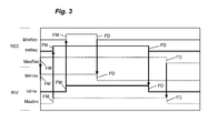
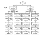
- the reasoning is the same starting from a pulse of the rectifier stage 1. In this way, it is thus possible to achieve a total synchronization of all the commutations by respecting specific selection rules such as those described herein. below in connection with the figure 4 .
- the first and second control means 3, 4 are configured so as to be able to move in time each voltage pulse generated by the switching arms respectively of the rectifier stage 1 and the inverter stage 2 .
- each rising voltage edge FM generated by the control of a switching arm 10a, 10b, 10c of the rectifier stage 1 is synchronized in time with the generation of a rising voltage edge FM produced by the control of a arm of switching 20a, 20b, 20c of the inverter stage 2.
- each falling voltage edge FD generated by the control of a switching arm 10a, 10b, 10c of the rectifier stage 1 is synchronized in time with the generation of a falling voltage edge FD produced by the control of a switching arm 20a, 20b, 20c of the inverter stage 2.
- This algorithm comprises several successive steps implemented by the control means 3, 4.
- a first comparison step E consists in determining whether the longest pulse MaxRec to be applied on the rectifier stage 1 is longer than the longest pulse Maxlnv to be applied on the inverter stage 2.
- the total synchronization as described above in connection with the figures 3 and 4 between the rectifier stage 1 and the inverter stage 2 is feasible for each switching period and operates systematically, the last two rising voltage edges being automatically synchronized.
- This is explained in particular by the fact that the sum of the widths of the pulses applied to the rectifier stage 1 is equal to the sum of the widths of the pulses applied to the inverter stage 2 and that, on the rectifier part, the widths impulse are added (course directed to the right on the figure 3 ) while the pulse widths on the inverter part are retreating (path directed to the left on the figure 3 ).
Landscapes
- Engineering & Computer Science (AREA)
- Power Engineering (AREA)
- Physics & Mathematics (AREA)
- Electromagnetism (AREA)
- Inverter Devices (AREA)
- Rectifiers (AREA)
Applications Claiming Priority (1)
| Application Number | Priority Date | Filing Date | Title |
|---|---|---|---|
| FR1057995A FR2965684B1 (fr) | 2010-10-04 | 2010-10-04 | Procede et systeme de commande pour reduire le courant de mode commun dans un convertisseur de puissance |
Publications (3)
| Publication Number | Publication Date |
|---|---|
| EP2442436A2 true EP2442436A2 (de) | 2012-04-18 |
| EP2442436A3 EP2442436A3 (de) | 2017-11-15 |
| EP2442436B1 EP2442436B1 (de) | 2018-10-24 |
Family
ID=43334496
Family Applications (1)
| Application Number | Title | Priority Date | Filing Date |
|---|---|---|---|
| EP11181530.4A Active EP2442436B1 (de) | 2010-10-04 | 2011-09-16 | Verfahren und Steuersystem zur allgemeinen Reduzierung des Stroms in einem Leistungswandler |
Country Status (6)
| Country | Link |
|---|---|
| US (1) | US8817499B2 (de) |
| EP (1) | EP2442436B1 (de) |
| JP (1) | JP5826579B2 (de) |
| CN (1) | CN102447400B (de) |
| ES (1) | ES2707231T3 (de) |
| FR (1) | FR2965684B1 (de) |
Cited By (4)
| Publication number | Priority date | Publication date | Assignee | Title |
|---|---|---|---|---|
| EP2833534A1 (de) | 2013-07-31 | 2015-02-04 | Schneider Toshiba Inverter Europe SAS | Antriebssystem mit aktivem Gleichrichter und Wechselrichter mit Pulsmodifikation zur Minimierung von Gleichtaktstörungen |
| EP3208924A1 (de) | 2016-02-18 | 2017-08-23 | Schneider Toshiba Inverter Europe SAS | Steuerverfahren und -system für eine anlage zur steuerung eines elektromotors |
| EP3232556A1 (de) | 2016-04-14 | 2017-10-18 | Schneider Toshiba Inverter Europe SAS | Steuerverfahren und -system für eine anlage zur steuerung eines elektromotors |
| EP3393026A1 (de) * | 2017-04-21 | 2018-10-24 | Senvion GmbH | Windenergieanlage mit über eine verbindungsleitung angeschlossenem umrichter |
Families Citing this family (21)
| Publication number | Priority date | Publication date | Assignee | Title |
|---|---|---|---|---|
| EP2642653A1 (de) * | 2012-03-20 | 2013-09-25 | C. & E. Fein GmbH | Treiberschaltung und Ansteuerverfahren |
| JP5883733B2 (ja) * | 2012-07-06 | 2016-03-15 | 株式会社日立製作所 | 電力変換装置 |
| US9425705B2 (en) | 2012-08-13 | 2016-08-23 | Rockwell Automation Technologies, Inc. | Method and apparatus for bypassing cascaded H-bridge (CHB) power cells and power sub cell for multilevel inverter |
| FR3002703B1 (fr) * | 2013-02-25 | 2017-07-21 | Schneider Toshiba Inverter Europe Sas | Dispositif de commande employe dans un systeme d'alimentation electrique a decoupage |
| US9240731B2 (en) | 2013-03-18 | 2016-01-19 | Rockwell Automation Technologies, Inc. | Power cell bypass method and apparatus for multilevel inverter |
| CN103199728B (zh) * | 2013-03-29 | 2015-02-04 | 北京交通大学 | 一种减小三相pwm变流器共模电压的调制方法 |
| FI125100B (en) | 2013-11-14 | 2015-06-15 | Abb Technology Oy | Method and apparatus for minimizing inverter current or common-mode voltage |
| US9520800B2 (en) * | 2014-01-09 | 2016-12-13 | Rockwell Automation Technologies, Inc. | Multilevel converter systems and methods with reduced common mode voltage |
| CN106537748B (zh) * | 2014-06-04 | 2019-12-10 | Abb瑞士股份有限公司 | 具有高机器侧共模电压的电气转换器 |
| US9559541B2 (en) | 2015-01-15 | 2017-01-31 | Rockwell Automation Technologies, Inc. | Modular multilevel converter and charging circuit therefor |
| CA2993115C (en) * | 2015-04-24 | 2021-08-10 | Epc Power Corporation | Power converter with controllable dc offset |
| US9748862B2 (en) | 2015-05-13 | 2017-08-29 | Rockwell Automation Technologies, Inc. | Sparse matrix multilevel actively clamped power converter |
| WO2018037499A1 (ja) * | 2016-08-24 | 2018-03-01 | 東芝三菱電機産業システム株式会社 | Pwmコンバータ用入力フィルタの通電評価試験装置 |
| US9812990B1 (en) | 2016-09-26 | 2017-11-07 | Rockwell Automation Technologies, Inc. | Spare on demand power cells for modular multilevel power converter |
| CN107968435B (zh) * | 2017-12-15 | 2022-01-25 | 远景能源有限公司 | 风力发电双绕组发电机系统共模电压抑制方法 |
| CN111869083B (zh) * | 2018-03-09 | 2023-07-07 | 东芝三菱电机产业系统株式会社 | 电力变换装置 |
| US10158299B1 (en) | 2018-04-18 | 2018-12-18 | Rockwell Automation Technologies, Inc. | Common voltage reduction for active front end drives |
| US11211879B2 (en) | 2019-09-23 | 2021-12-28 | Rockwell Automation Technologies, Inc. | Capacitor size reduction and lifetime extension for cascaded H-bridge drives |
| CN111884523B (zh) * | 2020-08-07 | 2021-11-19 | 浙江鲲悟科技有限公司 | 功率转换系统 |
| US11342878B1 (en) | 2021-04-09 | 2022-05-24 | Rockwell Automation Technologies, Inc. | Regenerative medium voltage drive (Cascaded H Bridge) with reduced number of sensors |
| US11533013B1 (en) * | 2021-07-29 | 2022-12-20 | Rivian Ip Holdings, Llc | Pulse width modulation clock synchronization |
Citations (2)
| Publication number | Priority date | Publication date | Assignee | Title |
|---|---|---|---|---|
| US6185115B1 (en) | 1998-11-17 | 2001-02-06 | Seung Ki Sul | Three-phase pulse width modulation method and system for alternating current motor |
| JP2003018853A (ja) | 2001-06-28 | 2003-01-17 | Fuji Electric Co Ltd | コモンモード電流低減方法 |
Family Cites Families (2)
| Publication number | Priority date | Publication date | Assignee | Title |
|---|---|---|---|---|
| US7920393B2 (en) * | 2007-06-01 | 2011-04-05 | Drs Power & Control Technologies, Inc. | Four pole neutral-point clamped three phase converter with low common mode voltage output |
| US7738267B1 (en) * | 2009-01-07 | 2010-06-15 | Rockwell Automation Technologies, Inc. | Systems and methods for common-mode voltage reduction in AC drives |
-
2010
- 2010-10-04 FR FR1057995A patent/FR2965684B1/fr not_active Expired - Fee Related
-
2011
- 2011-09-16 ES ES11181530T patent/ES2707231T3/es active Active
- 2011-09-16 EP EP11181530.4A patent/EP2442436B1/de active Active
- 2011-09-21 US US13/238,036 patent/US8817499B2/en active Active
- 2011-09-29 CN CN201110300746.0A patent/CN102447400B/zh active Active
- 2011-10-03 JP JP2011218952A patent/JP5826579B2/ja active Active
Patent Citations (2)
| Publication number | Priority date | Publication date | Assignee | Title |
|---|---|---|---|---|
| US6185115B1 (en) | 1998-11-17 | 2001-02-06 | Seung Ki Sul | Three-phase pulse width modulation method and system for alternating current motor |
| JP2003018853A (ja) | 2001-06-28 | 2003-01-17 | Fuji Electric Co Ltd | コモンモード電流低減方法 |
Cited By (4)
| Publication number | Priority date | Publication date | Assignee | Title |
|---|---|---|---|---|
| EP2833534A1 (de) | 2013-07-31 | 2015-02-04 | Schneider Toshiba Inverter Europe SAS | Antriebssystem mit aktivem Gleichrichter und Wechselrichter mit Pulsmodifikation zur Minimierung von Gleichtaktstörungen |
| EP3208924A1 (de) | 2016-02-18 | 2017-08-23 | Schneider Toshiba Inverter Europe SAS | Steuerverfahren und -system für eine anlage zur steuerung eines elektromotors |
| EP3232556A1 (de) | 2016-04-14 | 2017-10-18 | Schneider Toshiba Inverter Europe SAS | Steuerverfahren und -system für eine anlage zur steuerung eines elektromotors |
| EP3393026A1 (de) * | 2017-04-21 | 2018-10-24 | Senvion GmbH | Windenergieanlage mit über eine verbindungsleitung angeschlossenem umrichter |
Also Published As
| Publication number | Publication date |
|---|---|
| CN102447400A (zh) | 2012-05-09 |
| US8817499B2 (en) | 2014-08-26 |
| JP2012080765A (ja) | 2012-04-19 |
| JP5826579B2 (ja) | 2015-12-02 |
| FR2965684A1 (fr) | 2012-04-06 |
| ES2707231T3 (es) | 2019-04-03 |
| CN102447400B (zh) | 2014-09-17 |
| US20120081932A1 (en) | 2012-04-05 |
| EP2442436A3 (de) | 2017-11-15 |
| FR2965684B1 (fr) | 2012-09-07 |
| EP2442436B1 (de) | 2018-10-24 |
Similar Documents
| Publication | Publication Date | Title |
|---|---|---|
| EP2442436B1 (de) | Verfahren und Steuersystem zur allgemeinen Reduzierung des Stroms in einem Leistungswandler | |
| EP3232556B1 (de) | Steuerverfahren und -system für eine anlage zur steuerung eines elektromotors | |
| EP2142397B1 (de) | Vorrichtung und verfahren zur steuerung einer shunt-stromschaltung und hybridfahrzeug damit | |
| EP2355331B1 (de) | Wandlervorrichtung und mit einer solchen vorrichtung ausgerüstete unterbrechungslose versorgung | |
| EP2833534B1 (de) | Antriebssystem mit aktivem Gleichrichter und Wechselrichter mit Pulsmodifikation zur Minimierung von Gleichtaktstörungen | |
| EP2645569B1 (de) | Steuervorrichtung, die in einem Stromzuführungssystem mit Partitionierung verwendet wird | |
| EP0555432A1 (de) | Elektronische vorrichtung zur elektrischen energieumwandlung. | |
| EP3208924B1 (de) | Steuerverfahren und -system für eine anlage zur steuerung eines elektromotors | |
| EP2770636B1 (de) | Steuervorrichtung, die in einem Stromzuführungssystem mit Partitionierung verwendet wird | |
| WO2003018346A1 (fr) | Alimentation electrique a tensions multiples pour vehicule ferroviaire | |
| EP2595296B1 (de) | Steuersystem, das ein Wechselrichtermodul umfasst, das als aktiver Gleichrichter verwendet wird | |
| EP0344067A1 (de) | Linearisierungsverfahren für Gleichspannungswandler und Durchführung des Verfahrens | |
| EP1410488B1 (de) | Energieumwandlungseinrichtung | |
| EP2656492A2 (de) | Wechselstrom/gleichstromrichter mit verbessertem leistungsfaktor und verbesserter thdi | |
| EP2815501B1 (de) | Modul zur regenerierung von elektrischer energie für einen drehzahlvariator | |
| WO2016151223A1 (fr) | Onduleur pour source d'energie continue | |
| WO2025141145A1 (fr) | Convertisseur d'énergie électrique avec élément(s) piézoélectrique(s) et système électronique de conversion d'énergie électrique associé | |
| EP4387079A1 (de) | Steuerungssystem für einen spannungswandler | |
| EP1039622A1 (de) | Verfahren zur Versorgung von galvanische Trennung benötigender Ausrüstung und entsprechender Generator | |
| EP3391521A1 (de) | Verbesserte aufladungsvorrichtung zum aufladen von elektrischer ausrüstung, insbesondere eines elektrofahrzeugs | |
| EP2717445A1 (de) | Steuerungsverfahren in einem Leistungswandler zur Sicherstellung der Feststellbarkeit eines Kurzschlusses |
Legal Events
| Date | Code | Title | Description |
|---|---|---|---|
| PUAI | Public reference made under article 153(3) epc to a published international application that has entered the european phase |
Free format text: ORIGINAL CODE: 0009012 |
|
| AK | Designated contracting states |
Kind code of ref document: A2 Designated state(s): AL AT BE BG CH CY CZ DE DK EE ES FI FR GB GR HR HU IE IS IT LI LT LU LV MC MK MT NL NO PL PT RO RS SE SI SK SM TR |
|
| AX | Request for extension of the european patent |
Extension state: BA ME |
|
| PUAL | Search report despatched |
Free format text: ORIGINAL CODE: 0009013 |
|
| AK | Designated contracting states |
Kind code of ref document: A3 Designated state(s): AL AT BE BG CH CY CZ DE DK EE ES FI FR GB GR HR HU IE IS IT LI LT LU LV MC MK MT NL NO PL PT RO RS SE SI SK SM TR |
|
| AX | Request for extension of the european patent |
Extension state: BA ME |
|
| RIC1 | Information provided on ipc code assigned before grant |
Ipc: H02M 1/44 20070101ALI20171010BHEP Ipc: H02M 5/458 20060101AFI20171010BHEP |
|
| STAA | Information on the status of an ep patent application or granted ep patent |
Free format text: STATUS: REQUEST FOR EXAMINATION WAS MADE |
|
| 17P | Request for examination filed |
Effective date: 20180424 |
|
| RBV | Designated contracting states (corrected) |
Designated state(s): AL AT BE BG CH CY CZ DE DK EE ES FI FR GB GR HR HU IE IS IT LI LT LU LV MC MK MT NL NO PL PT RO RS SE SI SK SM TR |
|
| GRAP | Despatch of communication of intention to grant a patent |
Free format text: ORIGINAL CODE: EPIDOSNIGR1 |
|
| STAA | Information on the status of an ep patent application or granted ep patent |
Free format text: STATUS: GRANT OF PATENT IS INTENDED |
|
| INTG | Intention to grant announced |
Effective date: 20180709 |
|
| GRAS | Grant fee paid |
Free format text: ORIGINAL CODE: EPIDOSNIGR3 |
|
| GRAA | (expected) grant |
Free format text: ORIGINAL CODE: 0009210 |
|
| STAA | Information on the status of an ep patent application or granted ep patent |
Free format text: STATUS: THE PATENT HAS BEEN GRANTED |
|
| AK | Designated contracting states |
Kind code of ref document: B1 Designated state(s): AL AT BE BG CH CY CZ DE DK EE ES FI FR GB GR HR HU IE IS IT LI LT LU LV MC MK MT NL NO PL PT RO RS SE SI SK SM TR |
|
| REG | Reference to a national code |
Ref country code: GB Ref legal event code: FG4D Free format text: NOT ENGLISH |
|
| REG | Reference to a national code |
Ref country code: CH Ref legal event code: EP |
|
| REG | Reference to a national code |
Ref country code: IE Ref legal event code: FG4D Free format text: LANGUAGE OF EP DOCUMENT: FRENCH |
|
| REG | Reference to a national code |
Ref country code: AT Ref legal event code: REF Ref document number: 1057858 Country of ref document: AT Kind code of ref document: T Effective date: 20181115 |
|
| REG | Reference to a national code |
Ref country code: DE Ref legal event code: R096 Ref document number: 602011053150 Country of ref document: DE |
|
| REG | Reference to a national code |
Ref country code: NL Ref legal event code: MP Effective date: 20181024 |
|
| REG | Reference to a national code |
Ref country code: LT Ref legal event code: MG4D |
|
| REG | Reference to a national code |
Ref country code: AT Ref legal event code: MK05 Ref document number: 1057858 Country of ref document: AT Kind code of ref document: T Effective date: 20181024 |
|
| PG25 | Lapsed in a contracting state [announced via postgrant information from national office to epo] |
Ref country code: NL Free format text: LAPSE BECAUSE OF FAILURE TO SUBMIT A TRANSLATION OF THE DESCRIPTION OR TO PAY THE FEE WITHIN THE PRESCRIBED TIME-LIMIT Effective date: 20181024 |
|
| REG | Reference to a national code |
Ref country code: ES Ref legal event code: FG2A Ref document number: 2707231 Country of ref document: ES Kind code of ref document: T3 Effective date: 20190403 |
|
| PG25 | Lapsed in a contracting state [announced via postgrant information from national office to epo] |
Ref country code: IS Free format text: LAPSE BECAUSE OF FAILURE TO SUBMIT A TRANSLATION OF THE DESCRIPTION OR TO PAY THE FEE WITHIN THE PRESCRIBED TIME-LIMIT Effective date: 20190224 Ref country code: FI Free format text: LAPSE BECAUSE OF FAILURE TO SUBMIT A TRANSLATION OF THE DESCRIPTION OR TO PAY THE FEE WITHIN THE PRESCRIBED TIME-LIMIT Effective date: 20181024 Ref country code: NO Free format text: LAPSE BECAUSE OF FAILURE TO SUBMIT A TRANSLATION OF THE DESCRIPTION OR TO PAY THE FEE WITHIN THE PRESCRIBED TIME-LIMIT Effective date: 20190124 Ref country code: AT Free format text: LAPSE BECAUSE OF FAILURE TO SUBMIT A TRANSLATION OF THE DESCRIPTION OR TO PAY THE FEE WITHIN THE PRESCRIBED TIME-LIMIT Effective date: 20181024 Ref country code: LV Free format text: LAPSE BECAUSE OF FAILURE TO SUBMIT A TRANSLATION OF THE DESCRIPTION OR TO PAY THE FEE WITHIN THE PRESCRIBED TIME-LIMIT Effective date: 20181024 Ref country code: LT Free format text: LAPSE BECAUSE OF FAILURE TO SUBMIT A TRANSLATION OF THE DESCRIPTION OR TO PAY THE FEE WITHIN THE PRESCRIBED TIME-LIMIT Effective date: 20181024 Ref country code: BG Free format text: LAPSE BECAUSE OF FAILURE TO SUBMIT A TRANSLATION OF THE DESCRIPTION OR TO PAY THE FEE WITHIN THE PRESCRIBED TIME-LIMIT Effective date: 20190124 Ref country code: HR Free format text: LAPSE BECAUSE OF FAILURE TO SUBMIT A TRANSLATION OF THE DESCRIPTION OR TO PAY THE FEE WITHIN THE PRESCRIBED TIME-LIMIT Effective date: 20181024 Ref country code: PL Free format text: LAPSE BECAUSE OF FAILURE TO SUBMIT A TRANSLATION OF THE DESCRIPTION OR TO PAY THE FEE WITHIN THE PRESCRIBED TIME-LIMIT Effective date: 20181024 |
|
| PG25 | Lapsed in a contracting state [announced via postgrant information from national office to epo] |
Ref country code: AL Free format text: LAPSE BECAUSE OF FAILURE TO SUBMIT A TRANSLATION OF THE DESCRIPTION OR TO PAY THE FEE WITHIN THE PRESCRIBED TIME-LIMIT Effective date: 20181024 Ref country code: PT Free format text: LAPSE BECAUSE OF FAILURE TO SUBMIT A TRANSLATION OF THE DESCRIPTION OR TO PAY THE FEE WITHIN THE PRESCRIBED TIME-LIMIT Effective date: 20190224 Ref country code: SE Free format text: LAPSE BECAUSE OF FAILURE TO SUBMIT A TRANSLATION OF THE DESCRIPTION OR TO PAY THE FEE WITHIN THE PRESCRIBED TIME-LIMIT Effective date: 20181024 Ref country code: GR Free format text: LAPSE BECAUSE OF FAILURE TO SUBMIT A TRANSLATION OF THE DESCRIPTION OR TO PAY THE FEE WITHIN THE PRESCRIBED TIME-LIMIT Effective date: 20190125 Ref country code: RS Free format text: LAPSE BECAUSE OF FAILURE TO SUBMIT A TRANSLATION OF THE DESCRIPTION OR TO PAY THE FEE WITHIN THE PRESCRIBED TIME-LIMIT Effective date: 20181024 |
|
| REG | Reference to a national code |
Ref country code: DE Ref legal event code: R097 Ref document number: 602011053150 Country of ref document: DE |
|
| PG25 | Lapsed in a contracting state [announced via postgrant information from national office to epo] |
Ref country code: CZ Free format text: LAPSE BECAUSE OF FAILURE TO SUBMIT A TRANSLATION OF THE DESCRIPTION OR TO PAY THE FEE WITHIN THE PRESCRIBED TIME-LIMIT Effective date: 20181024 Ref country code: DK Free format text: LAPSE BECAUSE OF FAILURE TO SUBMIT A TRANSLATION OF THE DESCRIPTION OR TO PAY THE FEE WITHIN THE PRESCRIBED TIME-LIMIT Effective date: 20181024 |
|
| PG25 | Lapsed in a contracting state [announced via postgrant information from national office to epo] |
Ref country code: RO Free format text: LAPSE BECAUSE OF FAILURE TO SUBMIT A TRANSLATION OF THE DESCRIPTION OR TO PAY THE FEE WITHIN THE PRESCRIBED TIME-LIMIT Effective date: 20181024 Ref country code: SM Free format text: LAPSE BECAUSE OF FAILURE TO SUBMIT A TRANSLATION OF THE DESCRIPTION OR TO PAY THE FEE WITHIN THE PRESCRIBED TIME-LIMIT Effective date: 20181024 Ref country code: EE Free format text: LAPSE BECAUSE OF FAILURE TO SUBMIT A TRANSLATION OF THE DESCRIPTION OR TO PAY THE FEE WITHIN THE PRESCRIBED TIME-LIMIT Effective date: 20181024 Ref country code: SK Free format text: LAPSE BECAUSE OF FAILURE TO SUBMIT A TRANSLATION OF THE DESCRIPTION OR TO PAY THE FEE WITHIN THE PRESCRIBED TIME-LIMIT Effective date: 20181024 |
|
| PLBE | No opposition filed within time limit |
Free format text: ORIGINAL CODE: 0009261 |
|
| STAA | Information on the status of an ep patent application or granted ep patent |
Free format text: STATUS: NO OPPOSITION FILED WITHIN TIME LIMIT |
|
| 26N | No opposition filed |
Effective date: 20190725 |
|
| PG25 | Lapsed in a contracting state [announced via postgrant information from national office to epo] |
Ref country code: SI Free format text: LAPSE BECAUSE OF FAILURE TO SUBMIT A TRANSLATION OF THE DESCRIPTION OR TO PAY THE FEE WITHIN THE PRESCRIBED TIME-LIMIT Effective date: 20181024 |
|
| PG25 | Lapsed in a contracting state [announced via postgrant information from national office to epo] |
Ref country code: TR Free format text: LAPSE BECAUSE OF FAILURE TO SUBMIT A TRANSLATION OF THE DESCRIPTION OR TO PAY THE FEE WITHIN THE PRESCRIBED TIME-LIMIT Effective date: 20181024 |
|
| PG25 | Lapsed in a contracting state [announced via postgrant information from national office to epo] |
Ref country code: MC Free format text: LAPSE BECAUSE OF FAILURE TO SUBMIT A TRANSLATION OF THE DESCRIPTION OR TO PAY THE FEE WITHIN THE PRESCRIBED TIME-LIMIT Effective date: 20181024 |
|
| REG | Reference to a national code |
Ref country code: CH Ref legal event code: PL |
|
| PG25 | Lapsed in a contracting state [announced via postgrant information from national office to epo] |
Ref country code: IE Free format text: LAPSE BECAUSE OF NON-PAYMENT OF DUE FEES Effective date: 20190916 Ref country code: LU Free format text: LAPSE BECAUSE OF NON-PAYMENT OF DUE FEES Effective date: 20190916 Ref country code: CH Free format text: LAPSE BECAUSE OF NON-PAYMENT OF DUE FEES Effective date: 20190930 Ref country code: LI Free format text: LAPSE BECAUSE OF NON-PAYMENT OF DUE FEES Effective date: 20190930 |
|
| REG | Reference to a national code |
Ref country code: BE Ref legal event code: MM Effective date: 20190930 |
|
| PG25 | Lapsed in a contracting state [announced via postgrant information from national office to epo] |
Ref country code: BE Free format text: LAPSE BECAUSE OF NON-PAYMENT OF DUE FEES Effective date: 20190930 |
|
| PG25 | Lapsed in a contracting state [announced via postgrant information from national office to epo] |
Ref country code: CY Free format text: LAPSE BECAUSE OF FAILURE TO SUBMIT A TRANSLATION OF THE DESCRIPTION OR TO PAY THE FEE WITHIN THE PRESCRIBED TIME-LIMIT Effective date: 20181024 |
|
| PG25 | Lapsed in a contracting state [announced via postgrant information from national office to epo] |
Ref country code: HU Free format text: LAPSE BECAUSE OF FAILURE TO SUBMIT A TRANSLATION OF THE DESCRIPTION OR TO PAY THE FEE WITHIN THE PRESCRIBED TIME-LIMIT; INVALID AB INITIO Effective date: 20110916 Ref country code: MT Free format text: LAPSE BECAUSE OF FAILURE TO SUBMIT A TRANSLATION OF THE DESCRIPTION OR TO PAY THE FEE WITHIN THE PRESCRIBED TIME-LIMIT Effective date: 20181024 |
|
| PG25 | Lapsed in a contracting state [announced via postgrant information from national office to epo] |
Ref country code: MK Free format text: LAPSE BECAUSE OF FAILURE TO SUBMIT A TRANSLATION OF THE DESCRIPTION OR TO PAY THE FEE WITHIN THE PRESCRIBED TIME-LIMIT Effective date: 20181024 |
|
| PGFP | Annual fee paid to national office [announced via postgrant information from national office to epo] |
Ref country code: DE Payment date: 20250926 Year of fee payment: 15 |
|
| PGFP | Annual fee paid to national office [announced via postgrant information from national office to epo] |
Ref country code: IT Payment date: 20250922 Year of fee payment: 15 |
|
| PGFP | Annual fee paid to national office [announced via postgrant information from national office to epo] |
Ref country code: GB Payment date: 20250923 Year of fee payment: 15 |
|
| PGFP | Annual fee paid to national office [announced via postgrant information from national office to epo] |
Ref country code: FR Payment date: 20250925 Year of fee payment: 15 |
|
| PGFP | Annual fee paid to national office [announced via postgrant information from national office to epo] |
Ref country code: ES Payment date: 20251015 Year of fee payment: 15 |