EP2442437B1 - Stromwandler - Google Patents
Stromwandler Download PDFInfo
- Publication number
- EP2442437B1 EP2442437B1 EP10785983.7A EP10785983A EP2442437B1 EP 2442437 B1 EP2442437 B1 EP 2442437B1 EP 10785983 A EP10785983 A EP 10785983A EP 2442437 B1 EP2442437 B1 EP 2442437B1
- Authority
- EP
- European Patent Office
- Prior art keywords
- arm switching
- phases
- switching devices
- values
- currents
- Prior art date
- Legal status (The legal status is an assumption and is not a legal conclusion. Google has not performed a legal analysis and makes no representation as to the accuracy of the status listed.)
- Active
Links
Images


Classifications
-
- H—ELECTRICITY
- H02—GENERATION; CONVERSION OR DISTRIBUTION OF ELECTRIC POWER
- H02P—CONTROL OR REGULATION OF ELECTRIC MOTORS, ELECTRIC GENERATORS OR DYNAMO-ELECTRIC CONVERTERS; CONTROLLING TRANSFORMERS, REACTORS OR CHOKE COILS
- H02P6/00—Arrangements for controlling synchronous motors or other dynamo-electric motors using electronic commutation dependent on the rotor position; Electronic commutators therefor
- H02P6/14—Electronic commutators
- H02P6/16—Circuit arrangements for detecting position
- H02P6/18—Circuit arrangements for detecting position without separate position detecting elements
-
- H—ELECTRICITY
- H02—GENERATION; CONVERSION OR DISTRIBUTION OF ELECTRIC POWER
- H02M—APPARATUS FOR CONVERSION BETWEEN AC AND AC, BETWEEN AC AND DC, OR BETWEEN DC AND DC, AND FOR USE WITH MAINS OR SIMILAR POWER SUPPLY SYSTEMS; CONVERSION OF DC OR AC INPUT POWER INTO SURGE OUTPUT POWER; CONTROL OR REGULATION THEREOF
- H02M7/00—Conversion of AC power input into DC power output; Conversion of DC power input into AC power output
- H02M7/42—Conversion of DC power input into AC power output without possibility of reversal
- H02M7/44—Conversion of DC power input into AC power output without possibility of reversal by static converters
- H02M7/48—Conversion of DC power input into AC power output without possibility of reversal by static converters using discharge tubes with control electrode or semiconductor devices with control electrode
- H02M7/53—Conversion of DC power input into AC power output without possibility of reversal by static converters using discharge tubes with control electrode or semiconductor devices with control electrode using devices of a triode or transistor type requiring continuous application of a control signal
- H02M7/537—Conversion of DC power input into AC power output without possibility of reversal by static converters using discharge tubes with control electrode or semiconductor devices with control electrode using devices of a triode or transistor type requiring continuous application of a control signal using semiconductor devices only, e.g. single switched pulse inverters
- H02M7/539—Conversion of DC power input into AC power output without possibility of reversal by static converters using discharge tubes with control electrode or semiconductor devices with control electrode using devices of a triode or transistor type requiring continuous application of a control signal using semiconductor devices only, e.g. single switched pulse inverters with automatic control of output wave form or frequency
- H02M7/5395—Conversion of DC power input into AC power output without possibility of reversal by static converters using discharge tubes with control electrode or semiconductor devices with control electrode using devices of a triode or transistor type requiring continuous application of a control signal using semiconductor devices only, e.g. single switched pulse inverters with automatic control of output wave form or frequency by pulse-width modulation
-
- H—ELECTRICITY
- H02—GENERATION; CONVERSION OR DISTRIBUTION OF ELECTRIC POWER
- H02M—APPARATUS FOR CONVERSION BETWEEN AC AND AC, BETWEEN AC AND DC, OR BETWEEN DC AND DC, AND FOR USE WITH MAINS OR SIMILAR POWER SUPPLY SYSTEMS; CONVERSION OF DC OR AC INPUT POWER INTO SURGE OUTPUT POWER; CONTROL OR REGULATION THEREOF
- H02M7/00—Conversion of AC power input into DC power output; Conversion of DC power input into AC power output
- H02M7/66—Conversion of AC power input into DC power output; Conversion of DC power input into AC power output with possibility of reversal
- H02M7/68—Conversion of AC power input into DC power output; Conversion of DC power input into AC power output with possibility of reversal by static converters
- H02M7/72—Conversion of AC power input into DC power output; Conversion of DC power input into AC power output with possibility of reversal by static converters using discharge tubes with control electrode or semiconductor devices with control electrode
- H02M7/79—Conversion of AC power input into DC power output; Conversion of DC power input into AC power output with possibility of reversal by static converters using discharge tubes with control electrode or semiconductor devices with control electrode using devices of a triode or transistor type requiring continuous application of a control signal
- H02M7/797—Conversion of AC power input into DC power output; Conversion of DC power input into AC power output with possibility of reversal by static converters using discharge tubes with control electrode or semiconductor devices with control electrode using devices of a triode or transistor type requiring continuous application of a control signal using semiconductor devices only
-
- H—ELECTRICITY
- H02—GENERATION; CONVERSION OR DISTRIBUTION OF ELECTRIC POWER
- H02M—APPARATUS FOR CONVERSION BETWEEN AC AND AC, BETWEEN AC AND DC, OR BETWEEN DC AND DC, AND FOR USE WITH MAINS OR SIMILAR POWER SUPPLY SYSTEMS; CONVERSION OF DC OR AC INPUT POWER INTO SURGE OUTPUT POWER; CONTROL OR REGULATION THEREOF
- H02M1/00—Details of apparatus for conversion
- H02M1/0003—Details of control, feedback or regulation circuits
- H02M1/0009—Devices or circuits for detecting current in a converter
-
- H—ELECTRICITY
- H02—GENERATION; CONVERSION OR DISTRIBUTION OF ELECTRIC POWER
- H02P—CONTROL OR REGULATION OF ELECTRIC MOTORS, ELECTRIC GENERATORS OR DYNAMO-ELECTRIC CONVERTERS; CONTROLLING TRANSFORMERS, REACTORS OR CHOKE COILS
- H02P6/00—Arrangements for controlling synchronous motors or other dynamo-electric motors using electronic commutation dependent on the rotor position; Electronic commutators therefor
- H02P6/14—Electronic commutators
- H02P6/16—Circuit arrangements for detecting position
- H02P6/18—Circuit arrangements for detecting position without separate position detecting elements
- H02P6/183—Circuit arrangements for detecting position without separate position detecting elements using an injected high frequency signal
Definitions
- the present invention relates to a power converting apparatus which converts DC power into AC power by using a plurality of switching means, such as semiconductor switching devices, and in particular, the invention pertains to a related current detecting technique.
- a common method for detecting currents flowing in three phases of a three-phase inverter which serves as a power converting apparatus has been to detect currents of two phases by use of current sensors provided in two of the three phases and calculate a current of the remaining one phase utilizing the fact that the sum of the three-phase currents is zero, thereby detecting all of the three-phase currents.
- a method developed to solve this problem is to provide one current sensor in a DC bus line of an inverter and reproduce three-phase currents from a DC bus current and switching states of semiconductor switching devices of the inverter.
- the aforementioned method however has had a problem that if three-phase voltage commands are small or a difference between voltage commands for two phases among the three-phase voltage commands are small, the duration of time of the switching pattern becomes shorter, making it difficult to detect the currents.
- a method developed under such circumstances is to make such a correction that the difference among the three-phase voltage commands becomes large enough to detect the currents in a first half of each pulse width modulation (PWM) cycle as well as such a correction in a second half of each PWM cycle that an average of voltage commands in the first and second halves becomes equal to an original voltage command.
- PWM pulse width modulation
- Patent Documents 3 to 10 relate to the field of power conversion and current detection, and are considered particularly relevant to the teachings of the present application.
- the present invention has been made to solve the aforementioned problems. Accordingly, it is an object of the invention to obtain a power converting apparatus which makes it possible to reduce errors caused by differences in current detecting timings for individual phases when a simple current detecting method involving calculation of the currents of the individual phases on an AC side by use of a single current sensor provided on a DC side of an inverter is employed.
- the power converting apparatus including, in particular, the timing signal generator and the phase determination signal generator provided in the ON/OFF signal generating unit as well as the detected current correction unit corrects the detected current values detected by the current sensor at different timings for the individual phases to represent values which would be obtained at the same reference timing as described above. It is therefore possible to reliably obtain the detected current values for the individual phases containing reduced errors caused by differences in the detection timings.
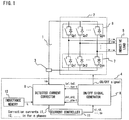
- FIG. 1 is a circuit configuration diagram illustrating the configuration of a power converting apparatus according to a first embodiment of the present invention.
- the power converting apparatus includes a DC power supply 1, an inverter 2, a current sensor 3 and a control section 4, and an output of the power converting apparatus is supplied to an inductive load 5.
- the inverter 2 includes upper-arm switching devices 6 for n phases (where n is an integer equal to or larger than 3), each of the upper-arm switching devices 6 having one end connected to a positive side of the DC power supply 1, and lower-arm switching devices 7 for the n phases connected in series with the upper-arm switching devices 6 of the respective phases, each of the lower-arm switching devices 7 having one end connected to a negative side of the DC power supply 1.
- the DC power supply 1 may be any of various devices like a battery, a diode rectifier circuit or a PWM converter, for instance.
- the control section 4 includes an ON/OFF signal generating unit 8, a detected current correction unit 9, a current control unit 11 and an inductance memory unit 12.
- the current control unit 11 receives correction currents i1, i2, ..., in for the n phases fed from the detected current correction unit 9 and outputs ON periods t1, t2, ..., tn of the upper-arm switching devices 6 for the individual phases in order to supply desired electric power to the inductive load 5.
- the ON/OFF signal generating unit 8 generates ON/OFF signals for turning on and off the upper-arm switching devices 6 designated by Qp1, Qp2, ..., Qpn and the lower-arm switching devices 7 designated by Qn1, Qn2, ..., Qnn.
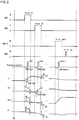
- Illustrated in FIG. 2 is an example of the ON/OFF signals.
- the ON/OFF signal When the ON/OFF signal is at a high (H) level, the relevant switching device is ON, and when the ON/OFF signal is at a low (L) level, the relevant switching device is OFF.
- Gp1, Gp2, ..., Gpn which denote signals for turning on and off the upper-arm switching devices 6 designated by Qp1, Qp2, ..., Qpn and Gn1, Gn2, ..., Gnn which denote signals for turning on and off the lower-arm switching devices 7 designated by Qn1, Qn2, ..., Qnn have a complementary relationship. Specifically, when Gp1 is H, Gn1 is L, for example.
- the ON periods t1, t2, ..., tn-1 have sufficient lengths to allow acquisition of detected current values from the current sensor 3, the ON period tn is so short that it is impossible to acquire any detected current value.
- i1, ... in are waveforms of currents of the individual phases that are output from the inverter 2 to the inductive load 5, the waveforms depicting how AC currents of the individual phases vary with voltages output from the inverter 2 in accordance with the ON/OFF signals.
- the ON/OFF signal generating unit 8 is provided with a timing signal generator for generating timing signals ts1, ts2, ..., tsn-1 used for setting timings at which the detected current values fed from the current sensor 3 are to be sampled and held in accordance with the ON/OFF signals as well as a phase determination signal generator for generating phase determination signals ph1, ph2, ..., phn-1 used for determining to which phase current each of currents detected by the current sensor 3 at the timings set in accordance with the timing signals corresponds.
- a timing signal generator for generating timing signals ts1, ts2, ..., tsn-1 used for setting timings at which the detected current values fed from the current sensor 3 are to be sampled and held in accordance with the ON/OFF signals as well as a phase determination signal generator for generating phase determination signals ph1, ph2, ..., phn-1 used for determining to which phase current each of currents detected by the current sensor 3 at the timings set in accordance with
- the current that can be detected by the current sensor 3 in accordance with the timing signal ts1 is a first-phase current i1
- the current that can be detected in accordance with the timing signal ts2 is a second-phase current i2, ...
- the current that can be detected in accordance with the timing signal tsn-1 is an (n-1)th-phase current in-1.
- an mth timing signal tsm (where m is an integer chosen from 1 to n) is delayed from a rise timing of an ON signal at which the ON/OFF signal becomes H in an mth place by as much as tdelaym.
- the detected current correction unit 9 is provided with a sample-and-hold portion and a current calculation portion.
- the sample-and-hold portion holds the detected current values fed from the current sensor 3 at corresponding points in time and outputs the same as DC hold currents idc1, idc2, ..., idcn-1.
- the current calculation portion of the detected current correction unit 9 performs a calculation for correcting AC-side currents of the individual phases in a later-described manner using the DC hold currents idc1, idc2, ..., idcn-1, the phase determination signals ph1, ph2, ..., phn-1 and inductance L of the inductive load 5 held in the inductance memory unit 12.
- the second-phase current i2 is determined from the DC hold current idc2, ...
- the (n-1)th-phase current in-1 is determined from the DC hold current idcn-1. Then, the nth-phase current in is determined utilizing the fact that the sum of currents flowing in the n phases is zero.
- the ON/OFF signals are generated in such a manner that the ON period of the upper-arm switching device 6 and that of the lower-arm switching device 7 of each phase do not overlap each other.
- the timing ts1 at which the first-phase current is detected for example, the upper-arm switching device Qp1 for the first phase is ON and all the other devices of the upper-arm switching devices 6 are OFF, whereas the lower-arm switching device Qnl for the first phase is OFF and all the other devices of the lower-arm switching devices 7 are ON.
- Vdc denotes voltage of the DC power supply 1
- Z denotes impedance of the inductive load 5 which is common for all of the individual phases.
- Equations (1) and (2) are divided by inductances of the individual phases, current change rates of the individual phases are obtained.
- the currents of the n-1 phases detected at different timings by the current sensor 3 provided on a DC side are corrected to have values which would be obtained at the same reference timing (t0) and the current of the nth phase is obtained by calculation on the basis of the sum of the corrected current values for the n-1 phases as described above. It is therefore possible to reduce errors.
- the invention is not limited to this method of selecting the reference timing.
- While the ON/OFF signals are generated in such a manner that the ON period of the upper-arm switching device 6 and that of the lower-arm switching device 7 of each phase do not overlap each other in the foregoing first embodiment, described in this second embodiment is how the currents are corrected when the ON periods for the individual phases partially overlap.
- FIG. 4 depicts ON/OFF signals generated by the ON/OFF signal generating unit 8 together with timing signals and AC currents.
- n the number of phases
- Signals Gp1, Gp2, Gp3 for turning on the upper-arm switching devices 6 become H at timings successively offset by as much as tmin from a situation where all of the signals Gp1, Gp2, Gp3 are at the L level, tmin representing a minimum time period necessary for determining an AC-side current from a detected value output from the current sensor 3.
- This minimum time period is determined by surge voltages and ringing time of a main inverter circuit as well as the performance of the current sensor, for example.
- a time period during which only the signal Gp1 is H, or only the upper-arm switching device Qp1 among the upper-arm switching devices 6 is on, is as long as the minimum time period tmin, and also a time period during which the signals Gp1 and Gp2 are H, or the upper-arm switching devices Qp1 and Qp2 are on, is as long as the minimum time period tmin. Therefore, it is possible to detect AC-side currents during the respective time periods in a reliable fashion.
- calculated currents for the three phases are obtained from the currents of the two phases detected during the time periods which are as long as the minimum time period tmin utilizing the fact that the sum of the three-phase currents is zero.
- the fact that the sum of the currents of the three phases becomes zero is true only if the currents of all the phases have values detected at the same time and, therefore, the currents detected in accordance with the timing signals ts1 and ts2 are corrected to represent current values at the reference timing (t0) indicated in FIG. 4 , for example. This correction may be made in the following fashion by the same method as used in the first embodiment.
- Equations (4) and (5) above are equivalent to each other when modified.
- the currents of the two phases detected at different timings by the current sensor 3 provided on the DC side are corrected to have values which would be obtained at the same reference timing (t0) and the current of the third phase is obtained by calculation on the basis of the sum of the corrected current values for the two phases as described above. It is therefore possible to reduce errors.
- the signals Gp1, Gp2, Gp3 for turning on the upper-arm switching devices may become H at timings successively offset by as much as tmin in any arbitrary order from the situation where all of the signals Gp1, Gp2, Gp3 are at the L level.
- a third embodiment of this invention is characterized in that the signals Gp1, Gp2, ..., Gpn for turning on the upper-arm switching devices 6 are so generated as to become H at timings successively offset by as much as tmin from a situation where all of the signals Gp1, Gp2, ..., Gpn are at the L level in order of phases with increasing lengths of the ON periods t1, t2, ..., tn that define time periods during which the respective upper-arm switching devices 6 are kept on.
- This arrangement if applied to the foregoing second embodiment, makes it possible to maximize the output voltages of the inverter 2.
- the signals Gp1, Gp2, Gp3 become H in order of increasing durations of the signals Gp1, Gp2, Gp3 and the ON periods.
- time periods during which the upper-arm switching devices 6 can be kept on is tc for the signal Gp1 for the first phase that first becomes on, tc - tmin for the signal Gp2 for the second phase that next becomes on, and tc - tmin ⁇ 2 for the signal Gp3 for the third phase that lastly becomes on.
- a fourth embodiment of this invention is characterized in that the order of phases in which the signals Gp1, Gp2, ..., Gpn for turning on the upper-arm switching devices 6 become H at timings successively offset by as much as tmin from a situation where all of the signals Gp1, Gp2, ..., Gpn are at the L level is periodically varied.
- This arrangement serves to smoothen frequencies of ripple currents induced by offsetting the timings at which the signals Gp1, Gp2, ..., Gpn become H, making it possible to reduce acoustic noise and vibrations caused by the ripple currents.
- the order in which the signals Gp1, Gp2, ..., Gpn become H is varied as shown in Table 1 which indicates a sequence of ON/OFF cycles in which the upper-arm switching devices 6 of the individual phases are turned on.
- the "sequence of ON/OFF cycles” is defined as a process of turning on and off each of the upper-arm switching devices 6 once bringing the same from a state in which all of the upper-arm switching devices 6 are in an OFF state back to the state in which all of the upper-arm switching devices 6 are in the OFF state.
- the sequence returns to the first ON/OFF cycle after the third ON/OFF cycle.
- the order in which the signal Gp1 for the first phase becomes H is as follows: first in the first ON/OFF cycle, third in the second ON/OFF cycle, second in the third ON/OFF cycle, and first again in the subsequent first ON/OFF cycle.
- Table 1 ON/OFF cycles Cycle 1 Cycle 2 Cycle 3 1st phase 1 3 2 2nd phase 2 1 3 3rd phase 3 2 1
- ripple currents oriented in the same directions are always induced in the same phases in the AC currents i1, i2, i3,
- ripple currents are uniformly distributed in the individual phases, forming smooth waveforms in which the ripple currents are oriented in positive and negative directions in a repetitive pattern. It is therefore possible to reduce acoustic noise and vibrations caused by the ripple currents.
- While the order in which the signals Gp1, Gp2, ..., Gpn become H is periodically varied every three ON/OFF cycles as discussed above, the invention is not limited thereto.
- the order in which the signals Gp1, Gp2, ..., Gpn become H may be varied every six ON/OFF cycles as shown in Table 2.
- FIG. 8 illustrates the configuration of a power converting apparatus according to a fifth embodiment of the present invention.
- the fifth embodiment differs from the foregoing first to fourth embodiments in that the inductive load is a rotary machine 13, there is provided a rotor position estimator 14, and the current control unit 11 operates in a different way.
- This arrangement makes it possible to perform control operation for setting the rotary machine 13 in desired conditions in terms of torque, speed and rotor position, for example, by estimating the rotor position of the rotary machine 13 without the provision of a position sensor mounted on the rotary machine 13.
- the current control unit 11 outputs ON periods t1, t2, ..., tn during which the upper-arm switching devices 6 are kept on in order to control the rotary machine 13 to reach the desired conditions and apply voltages containing a later-described frequency component ⁇ h differing from an operating frequency of the rotary machine 13 on the basis of the correction currents for the n phases fed from the detected current correction unit 9 and estimated rotor position ⁇ e of the rotary machine output from the rotor position estimator 14.
- rotor position estimator 14 calculates the estimated rotor position ⁇ e.
- Position information ⁇ is contained in amplitudes of the currents i ⁇ s, i ⁇ s expressed by fixed Cartesian coordinates as indicated in Equations (10) above, and the estimated rotor position ⁇ e can be calculated from this information,
- the amplitudes I ⁇ s, I ⁇ s of the currents i ⁇ s, i ⁇ s expressed by fixed Cartesian coordinates are extracted by Fourier transform. Then, using the extracted amplitudes I ⁇ s, I ⁇ s, a calculation indicated in Equation (11) below is performed to extract a term containing only the position information ⁇ .
- the estimated rotor position ⁇ e may be determined from the position information ⁇ obtained on the basis of a value of cos2 ⁇ stored in a memory device having a table holding values of cos2 ⁇ prepared in advance instead of calculating the arc cosine of cos2 ⁇ .
- the rotor position of the rotary machine can be calculated by using only the rotary machine currents detected by applying the foregoing embodiments and, therefore, the present embodiment is advantageous in that computational complexity can be reduced. It should be noted however that the invention is not limited to the aforementioned rotor position calculating procedure.
- the AC currents are corrected on the basis of the value of the voltage of the DC power supply 1 and the value of the inductance of the inductive load 5 in the foregoing individual embodiments, more accurate values of the AC currents will be obtained in the case where the inductive load 5 is the rotary machine 13 if the AC currents are corrected on the basis of the value of a voltage including the voltage of the DC power supply 1 and a voltage induced in the rotary machine 13 and the value of the inductance of the inductive load 5.
- the ON/OFF signals for the inverter 2 are generated by using the correction currents for the n phases fed from the detected current correction unit 9 in the foregoing individual embodiments, the inverter 2 may be operated by using predefined ON/OFF signals while just examining the correction currents for the n phases.
- the present invention is widely applicable to power converting apparatuses provided with various kinds of inverters,
- the invention makes it possible to detect AC currents of individual phases with high accuracy by use of simple and inexpensive means and to perform various control operations by using thus detected current values.
Landscapes
- Engineering & Computer Science (AREA)
- Power Engineering (AREA)
- Inverter Devices (AREA)
Claims (8)
- Leistungsumwandlungsvorrichtung, die Folgendes aufweist:- eine Gleichstromversorgung (1);- einen Wechselrichter (2), der Folgendes aufweist: Oberarm-Schalteinrichtungen (6) für 3 Phasen, wobei jede der Oberarm-Schalteinrichtungen (6) ein Ende aufweist, das mit einer positiven Seite der Gleichstromversorgung (1) verbunden ist; und Unterarm-Schalteinrichtungen (7) für die 3 Phasen, die in Reihe mit den Oberarm-Schalteinrichtungen (6) der jeweiligen Phasen geschaltet sind, wobei jede der Unterarm-Schalteinrichtungen (7) ein Ende aufweist, das mit einer negativen Seite der Gleichstromversorgung (1) verbunden ist, wobei der Wechselrichter (2) dazu ausgebildet ist, Wechselspannungen für die 3 Phasen an eine induktive Last (5) zu liefern, die mit Verbindungspunkten zwischen den Oberarm-Schalteinrichtungen (6) und den Unterarm-Schalteinrichtungen (7) der einzelnen Phasen verbunden ist, und zwar durch das Steuern der Oberarm-Schalteinrichtungen (6) und der Unterarm-Schalteinrichtungen (7), so dass diese einschalten und ausschalten;- einen Stromsensor (3), der dazu ausgebildet ist, Strom zu detektieren, der zwischen der Gleichstromversorgung (1) und dem Wechselrichter (2) fließt; und- eine EIN/AUS-Signalerzeugungseinheit (8), die dazu ausgebildet ist, EIN/AUS-Signale an die Oberarm-Schalteinrichtungen (6) und die Unterarm-Schalteinrichtungen (7) auszugeben;- wobei die Leistungsumwandlungsvorrichtung ferner Folgendes aufweist:- einen Zeitsignalgenerator, der in der EIN/AUS-Signalerzeugungseinheit (8) angeordnet und dazu ausgebildet ist, Zeitsignale zu erzeugen, die zum Vorgeben von Zeitpunkten verwendet werden, bei denen Ströme der einzelnen Phasen, die in die induktive Last (5) fließen, detektiert werden;- einen Phasenbestimmungssignalgenerator, der in der EIN/AUS-Signalerzeugungseinheit (8) angeordnet ist und dazu ausgebildet ist, Phasenbestimmungssignale zu erzeugen, die zum Bestimmen der Phase des Stroms verwendet werden, der zu jedem der durch die Zeitsignale vorgegebenen Zeitpunkte in dem Stromsensor (3) fließt; und- eine Detektierter-Strom-Korrektureinheit (9), die dazu ausgebildet ist, detektierte Stromwerte, die von dem Stromsensor (3) zu den durch die Zeitsignale vorgegeben Zeitpunkten zugeführt werden, und Phasen der detektierten Stromwerte zu bestimmen, und zwar basierend auf den Zeitsignalen und den Phasenbestimmungssignalen, und die detektierten Stromwerte für die einzelnen Phasen zu korrigieren, die zu den einzelnen Zeitpunkten während bestimmter Zeitspannen erhalten werden, um Werte darzustellen, die zu einem bestimmten Referenzzeitpunkt erhalten würden,- wobei die EIN/AUS-Signalerzeugungseinheit (8) dazu ausgebildet ist, die EIN/AUS-Signale zu erzeugen, die bewirken, dass die Oberarm-Schalteinrichtungen (6) oder die Unterarm-Schalteinrichtungen (7) der einzelnen Phasen in bestimmten Zeitintervallen nacheinander eingeschaltet werden, und zwar aus einem Zustand, in dem sich die Oberarm-Schalteinrichtungen (6) oder die Unterarm-Schalteinrichtungen (7) von allen Phasen in einem AUS-Zustand befinden, und wobei der Zeitsignalgenerator dazu ausgebildet ist, die Zeitsignale zu erzeugen, bei denen die Ströme der einzelnen Phasen in den bestimmten Zeitintervallen der bestimmten Zeitspannen detektiert werden,
dadurch gekennzeichnet,
dass die EIN/AUS-Signalerzeugungseinheit (8) dazu ausgebildet ist, die Reihenfolge der Phasen zu variieren, in der die Oberarm-Schalteinrichtungen (6) oder die Unterarm-Schalteinrichtungen (7) nacheinander eingeschaltet werden, und zwar in jedem PWM-Intervall, wobei dieser Reihenfolgenänderungs-Zyklus in jedem Intervall des ganzzahligen Vielfachen von 3 oder 6 des PWM-Intervalls wiederholt wird und die spezifischen Zeitintervalle, um die die Einschaltsignale nacheinander versetzt sind, eine Mindestzeitspanne (tmin) ist, die zum Bestimmen eines wechselstromseitigen Stroms aus einem von dem Stromsensor (3) ausgegebenen detektierten Wert erforderlich ist, wobei diese Mindestzeitspanne (tmin) durch Stoßspannungen und Rufzeiten einer Hauptwechselrichterschaltung sowie die Leistung des Stromsensors bestimmt wird. - Leistungsumwandlungsvorrichtung nach Anspruch 1,
wobei die Detektierter-Strom-Korrektureinheit (9) dazu ausgebildet ist, die detektierten Stromwerte für die einzelnen Phasen zu korrigieren, die zu den einzelnen Zeitpunkten während der spezifischen Zeitspannen erhalten werden, um die Werte darzustellen, die zu dem spezifischen Referenzzeitpunkt erhalten würden, und zwar basierend auf einem Spannungswert der Gleichstromversorgung (1) und einem Induktivitätswertes der induktiven Last (5). - Leistungsumwandlungsvorrichtung nach Anspruch 1 oder 2,
wobei die induktive Last (5) eine rotierende Maschine ist und die Detektierter-Strom-Korrektureinheit (9) dazu ausgebildet ist, die detektierten Stromwerte für die einzelnen Phasen zu korrigieren, die zu den einzelnen Zeitpunkten während der spezifischen Zeitspannen erhalten werden, um die Werte darzustellen, die zu dem spezifischen Referenzzeitpunkt erhalten würden, und zwar basierend auf einem Spannungswert der Gleichstromversorgung (1), einem induzierten Spannungswert der rotierenden Maschine und einem Induktivitätswert der induktiven Last (5). - Leistungsumwandlungsvorrichtung nach einem der Ansprüche 1 bis 3,
wobei der Wechselrichter (2) dazu ausgebildet ist, eine Pulsweitenmodulation (13WM)-Steuerung anzuwenden, und die Detektierter-Strom-Korrektureinheit (9) dazu ausgebildet ist, die detektierten Stromwerte für die einzelnen Phasen zu korrigieren, die zu den einzelnen Zeitpunkten während aufeinanderfolgender PWM-Zyklen in Intervallen der PW1VI-Zyklen erhalten werden, um die Werte darzustellen, die zu dem spezifischen Referenzzeitpunkt erhalten würden. - Leistungsumwandlungsvorrichtung nach Anspruch 1,
wobei die EIN/AUS-Signalerzeugungseinheit (8) dazu ausgebildet ist, die EIN-Zeitspannen der Oberarm-Schalteinrichtung (6) und der Unterarm-Schalteinrichtung (7) von jeder Phase so anzuordnen, dass sie sich nicht gegenseitig überlagern. - Leistungsumwandlungsvorrichtung nach Anspruch 1,
wobei die Ströme von n-1 Phasen von den Ströme der n-Phasen durch die von der Detektierter-Strom-Korrektureinheit (9) korrigierten Stromwerte ausgedrückt werden, um die Werte darzustellen, die zu dem spezifischen Referenzzeitpunkt erhalten würden, und wobei der Strom der verbleibenden einen Phase durch den Wert ausgedrückt wird, der gleich
(die Summe der korrigierten Stromwerte für die n-1-Phasen) x(-1) ist. - Leistungsumwandlungsvorrichtung nach einem der Ansprüche 1 bis 6, die ferner eine Stromsteuereinheit (11) zum Berechnen von EIN-Zeitspannen der Oberarm-Schalteinrichtung (6) und der Unterarm-Schalteinrichtung (7) der einzelnen Phasen aufweist, und zwar basierend auf den detektierten Stromwerten für die einzelnen Phasen, die von der Detektierter-Strom-Korrektureinheit (9) korrigiert werden, um die Werte darzustellen, die zu dem spezifischen Referenzzeitpunkt erhalten würden, und zum Ausgeben der EIN-Zeitspannen an die EIN/AUS-Signalerzeugungseinheit (8), so dass gewünschte Wechselspannungen für die n Phasen an die induktive Last (5) geliefert werden.
- Leistungsumwandlungsvorrichtung nach einem der Ansprüche 1 bis 7, wobei die induktive Last (5) eine rotierende Maschine ist und die EIN/AUS-Signalerzeugungseinheit (8) dazu ausgebildet ist, die EIN/AUS-Signale derart zu erzeugen, dass die Ausgangsspannungen des Wechselrichters (2) mit einer Spannungskomponente mit einer von einer Betriebsfrequenz der rotierenden Maschine abweichenden Frequenz überlagert werden; und- wobei die Leistungsumwandlungsvorrichtung ferner einen Rotorpositionsschätzer (14) zum Berechnen einer geschätzten Rotorposition der rotierenden Maschine aufweist, und zwar basierend auf der Frequenzkomponente der überlagerten Spannung, die aus den detektierten Stromwerten für die einzelnen Phasen extrahiert wird, die von der Detektierter-Strom-Korrektureinheit (4) korrigiert werden, um die Werte darzustellen, die bei dem spezifischen Referenzzeitpunkt erhalten würden.
Applications Claiming Priority (2)
| Application Number | Priority Date | Filing Date | Title |
|---|---|---|---|
| JP2009137053 | 2009-06-08 | ||
| PCT/JP2010/051839 WO2010143452A1 (ja) | 2009-06-08 | 2010-02-09 | 電力変換装置 |
Publications (3)
| Publication Number | Publication Date |
|---|---|
| EP2442437A1 EP2442437A1 (de) | 2012-04-18 |
| EP2442437A4 EP2442437A4 (de) | 2014-12-31 |
| EP2442437B1 true EP2442437B1 (de) | 2019-12-18 |
Family
ID=43308712
Family Applications (1)
| Application Number | Title | Priority Date | Filing Date |
|---|---|---|---|
| EP10785983.7A Active EP2442437B1 (de) | 2009-06-08 | 2010-02-09 | Stromwandler |
Country Status (5)
| Country | Link |
|---|---|
| US (1) | US8878482B2 (de) |
| EP (1) | EP2442437B1 (de) |
| JP (1) | JP5289567B2 (de) |
| CN (1) | CN102460934B (de) |
| WO (1) | WO2010143452A1 (de) |
Families Citing this family (10)
| Publication number | Priority date | Publication date | Assignee | Title |
|---|---|---|---|---|
| JP5724776B2 (ja) * | 2011-09-12 | 2015-05-27 | 日本精工株式会社 | モータ制御装置及び電動パワーステアリング装置 |
| JP5853641B2 (ja) * | 2011-11-28 | 2016-02-09 | ダイキン工業株式会社 | 線電流検出装置および電力変換システム |
| JP5853644B2 (ja) * | 2011-11-28 | 2016-02-09 | ダイキン工業株式会社 | 線電流検出装置および電力変換システム |
| GB2512078A (en) * | 2013-03-19 | 2014-09-24 | Control Tech Ltd | Control system for multi-phase rotary machines |
| CN104467505B (zh) * | 2014-11-28 | 2017-12-29 | 佛山市众盈电子有限公司 | 一种调宽逆变电路 |
| JP6372424B2 (ja) * | 2015-06-05 | 2018-08-15 | 株式会社安川電機 | 電力変換装置および電流検出方法 |
| JP6475182B2 (ja) * | 2016-03-28 | 2019-02-27 | ミネベアミツミ株式会社 | モータ駆動制御装置 |
| JP6749472B2 (ja) * | 2017-03-27 | 2020-09-02 | 三菱電機株式会社 | 回転電機の制御装置 |
| EP3427910B1 (de) * | 2017-07-14 | 2020-08-19 | Braun GmbH | Verfahren zur festlegung des zeitpunktverhaltens eines cyclischen motorverfahrens während der verwendung einer elektrischen haarentfernungsvorrichtung und haarentfernungsvorrichtung |
| JP7734543B2 (ja) * | 2021-09-17 | 2025-09-05 | 株式会社日立インダストリアルプロダクツ | 電力変換装置 |
Citations (1)
| Publication number | Priority date | Publication date | Assignee | Title |
|---|---|---|---|---|
| DE102006052467A1 (de) * | 2006-11-07 | 2008-05-08 | Robert Bosch Gmbh | Verfahren und Vorrichtung zur Strommessung in einem insbesondere mehrphasigen Stromnetz |
Family Cites Families (19)
| Publication number | Priority date | Publication date | Assignee | Title |
|---|---|---|---|---|
| JP2712470B2 (ja) | 1989-01-23 | 1998-02-10 | 松下電器産業株式会社 | インバータ装置の電流検出装置 |
| JP3296729B2 (ja) * | 1996-08-23 | 2002-07-02 | 本田技研工業株式会社 | 交流モータ制御装置 |
| JP3664040B2 (ja) | 2000-05-17 | 2005-06-22 | 日産自動車株式会社 | モータ制御用pwmインバータ |
| JP4880828B2 (ja) * | 2001-06-19 | 2012-02-22 | 株式会社東芝 | インバータ装置 |
| JP4367130B2 (ja) * | 2001-09-29 | 2009-11-18 | ダイキン工業株式会社 | 相電流検出方法、インバータ制御方法、モータ制御方法およびこれらの装置 |
| GB0220401D0 (en) * | 2002-09-03 | 2002-10-09 | Trw Ltd | Motor drive control |
| JP4055992B2 (ja) | 2002-12-25 | 2008-03-05 | サンデン株式会社 | インバータの電流検出装置 |
| JP2005192335A (ja) | 2003-12-25 | 2005-07-14 | Toyota Industries Corp | インバータ装置およびモータ制御方法 |
| JP4422567B2 (ja) * | 2004-06-30 | 2010-02-24 | 株式会社日立製作所 | モータ駆動装置,電動アクチュエータおよび電動パワーステアリング装置 |
| WO2006022142A1 (ja) * | 2004-08-27 | 2006-03-02 | Mitsubishi Denki Kabushiki Kaisha | 3相pwm信号発生装置 |
| US7560897B2 (en) * | 2005-03-29 | 2009-07-14 | Kabushiki Kaisha Yaskawa Denki | Current controller and current offset correction |
| JP4497149B2 (ja) | 2005-12-16 | 2010-07-07 | パナソニック株式会社 | インバータ装置 |
| US7193388B1 (en) * | 2006-02-02 | 2007-03-20 | Emerson Electric Co. | Offset PWM signals for multiphase motor |
| JP4082438B2 (ja) * | 2006-08-30 | 2008-04-30 | ダイキン工業株式会社 | 電流制御形電力変換装置 |
| ATE476010T1 (de) * | 2007-01-12 | 2010-08-15 | Abb Oy | Verfahren zur schätzung der rotordrehzahl und position einer synchronen permanentmagnetmaschine ohne lagegeber |
| JP4913661B2 (ja) * | 2007-04-26 | 2012-04-11 | ルネサスエレクトロニクス株式会社 | インバータ装置及びそれに用いられる半導体装置。 |
| JP5014034B2 (ja) * | 2007-09-12 | 2012-08-29 | オムロンオートモーティブエレクトロニクス株式会社 | 多相交流モータ駆動装置 |
| TWI347737B (en) * | 2008-02-27 | 2011-08-21 | Prolific Technology Inc | Method and pwm system of adjusting the width of pulses through collecting information of a three-phase current |
| JP4746667B2 (ja) * | 2008-11-26 | 2011-08-10 | 本田技研工業株式会社 | 電動機の相電流推定装置および電動機の磁極位置推定装置 |
-
2010
- 2010-02-09 US US13/318,812 patent/US8878482B2/en active Active
- 2010-02-09 CN CN201080025294.3A patent/CN102460934B/zh active Active
- 2010-02-09 JP JP2011518323A patent/JP5289567B2/ja active Active
- 2010-02-09 EP EP10785983.7A patent/EP2442437B1/de active Active
- 2010-02-09 WO PCT/JP2010/051839 patent/WO2010143452A1/ja not_active Ceased
Patent Citations (1)
| Publication number | Priority date | Publication date | Assignee | Title |
|---|---|---|---|---|
| DE102006052467A1 (de) * | 2006-11-07 | 2008-05-08 | Robert Bosch Gmbh | Verfahren und Vorrichtung zur Strommessung in einem insbesondere mehrphasigen Stromnetz |
Non-Patent Citations (4)
| Title |
|---|
| BLAABJERG F ET AL: "An ideal PWM-VSI inverter using only one current sensor in the DC-link", 19940101, 1 January 1994 (1994-01-01), pages 458 - 464, XP006511326 * |
| HYUNG-SUN RYU ET AL: "Carrier-Based Signal Injection Method for Harmonic Suppression in PWM Inverter Using Single DC-link Current Sensor", IEEE INDUSTRIAL ELECTRONICS, IECON 2006 - 32ND ANNUAL CONFERENCE ON, IEEE, PISCATAWAY, NJ, USA, 1 November 2006 (2006-11-01), pages 2700 - 2705, XP031077104, ISBN: 978-1-4244-0135-2 * |
| RIEDER U-H ET AL: "Sensorless control of an external rotor PMSM in the wholespeed range including standstill using DC-link measurements only", POWER ELECTRONICS SPECIALISTS CONFERENCE, 2004. PESC 04. 2004 IEEE 35TH ANNUAL, AACHEN, GERMANY 20-25 JUNE 2004, PISCATAWAY, NJ, USA,IEEE, US, 20 June 2004 (2004-06-20), pages 1280 - 1285, XP010739678, ISBN: 978-0-7803-8399-9, DOI: 10.1109/PESC.2004.1355606 * |
| WOO-CHEOL LEE ET AL: "Comparison of single-sensor current control in the DC link for three-phase voltage-source PWM converters", IEEE TRANSACTIONS ON INDUSTRIAL ELECTRONICS., vol. 48, no. 3, 1 June 2001 (2001-06-01), USA, pages 491 - 505, XP055269284, ISSN: 0278-0046, DOI: 10.1109/41.925576 * |
Also Published As
| Publication number | Publication date |
|---|---|
| CN102460934A (zh) | 2012-05-16 |
| JPWO2010143452A1 (ja) | 2012-11-22 |
| US8878482B2 (en) | 2014-11-04 |
| EP2442437A1 (de) | 2012-04-18 |
| WO2010143452A1 (ja) | 2010-12-16 |
| CN102460934B (zh) | 2014-10-15 |
| US20120049778A1 (en) | 2012-03-01 |
| EP2442437A4 (de) | 2014-12-31 |
| JP5289567B2 (ja) | 2013-09-11 |
Similar Documents
| Publication | Publication Date | Title |
|---|---|---|
| EP2442437B1 (de) | Stromwandler | |
| US7679309B2 (en) | Method and system for motor control with delay compensation | |
| CN102474208B (zh) | 电动机驱动装置的控制装置 | |
| JP6735827B2 (ja) | 電力変換装置 | |
| US20070296371A1 (en) | Position sensorless control apparatus for synchronous motor | |
| EP3288174B1 (de) | Steuerungsvorrichtung und steuerungsverfahren | |
| US20160190972A1 (en) | Power conversion device | |
| US20130334993A1 (en) | Methods, systems and apparatus for estimating angular position and/or angular velocity of a rotor of an electric machine | |
| AU2008305943A1 (en) | Controller of rotary electric machine | |
| US10608572B2 (en) | Motor drive control device | |
| EP2790317B1 (de) | Stromwandler | |
| CN106487265A (zh) | 电力变换装置、相电流检测装置以及相电流检测方法 | |
| US12184206B2 (en) | Controller for rotary electric machine | |
| JP2010246260A (ja) | モータ制御装置およびモータ制御方法 | |
| JP2018153028A (ja) | 集積回路 | |
| WO2012066800A1 (ja) | 電流検出装置及びモータ制御装置 | |
| JP3805637B2 (ja) | 電動機制御装置 | |
| US9935575B2 (en) | Power conversion device and control method for same, and electric power steering control device | |
| JP6116449B2 (ja) | 電動機駆動制御装置 | |
| US9948220B2 (en) | Rotation angle estimation apparatus for rotating electric machine | |
| CN113039717A (zh) | 交流旋转电机控制装置 | |
| JPH06189578A (ja) | 電圧形多相pwmインバータの制御装置 | |
| JP5931543B2 (ja) | モータシステム、モータ制御装置及びモータ制御方法 | |
| JP7314103B2 (ja) | 電動機の制御装置 | |
| JP2003274688A (ja) | インバータ制御方法およびその装置 |
Legal Events
| Date | Code | Title | Description |
|---|---|---|---|
| PUAI | Public reference made under article 153(3) epc to a published international application that has entered the european phase |
Free format text: ORIGINAL CODE: 0009012 |
|
| 17P | Request for examination filed |
Effective date: 20111207 |
|
| AK | Designated contracting states |
Kind code of ref document: A1 Designated state(s): AT BE BG CH CY CZ DE DK EE ES FI FR GB GR HR HU IE IS IT LI LT LU LV MC MK MT NL NO PL PT RO SE SI SK SM TR |
|
| DAX | Request for extension of the european patent (deleted) | ||
| A4 | Supplementary search report drawn up and despatched |
Effective date: 20141201 |
|
| RIC1 | Information provided on ipc code assigned before grant |
Ipc: H02P 6/18 20060101ALN20141125BHEP Ipc: H02M 1/00 20070101ALI20141125BHEP Ipc: H02M 7/5395 20060101AFI20141125BHEP |
|
| 17Q | First examination report despatched |
Effective date: 20150924 |
|
| STAA | Information on the status of an ep patent application or granted ep patent |
Free format text: STATUS: EXAMINATION IS IN PROGRESS |
|
| GRAP | Despatch of communication of intention to grant a patent |
Free format text: ORIGINAL CODE: EPIDOSNIGR1 |
|
| STAA | Information on the status of an ep patent application or granted ep patent |
Free format text: STATUS: GRANT OF PATENT IS INTENDED |
|
| RIC1 | Information provided on ipc code assigned before grant |
Ipc: H02M 1/00 20060101ALN20190121BHEP Ipc: H02P 6/18 20160101ALN20190121BHEP Ipc: H02M 7/5395 20060101AFI20190121BHEP Ipc: H02M 7/797 20060101ALI20190121BHEP |
|
| INTG | Intention to grant announced |
Effective date: 20190211 |
|
| REG | Reference to a national code |
Ref country code: DE Ref legal event code: R079 Ref document number: 602010062440 Country of ref document: DE Free format text: PREVIOUS MAIN CLASS: H02M0007538700 Ipc: H02M0007539500 |
|
| GRAJ | Information related to disapproval of communication of intention to grant by the applicant or resumption of examination proceedings by the epo deleted |
Free format text: ORIGINAL CODE: EPIDOSDIGR1 |
|
| STAA | Information on the status of an ep patent application or granted ep patent |
Free format text: STATUS: EXAMINATION IS IN PROGRESS |
|
| GRAP | Despatch of communication of intention to grant a patent |
Free format text: ORIGINAL CODE: EPIDOSNIGR1 |
|
| STAA | Information on the status of an ep patent application or granted ep patent |
Free format text: STATUS: GRANT OF PATENT IS INTENDED |
|
| INTC | Intention to grant announced (deleted) | ||
| RIC1 | Information provided on ipc code assigned before grant |
Ipc: H02M 7/5395 20060101AFI20190620BHEP Ipc: H02M 7/797 20060101ALI20190620BHEP Ipc: H02M 1/00 20060101ALN20190620BHEP Ipc: H02P 6/18 20160101ALN20190620BHEP |
|
| INTG | Intention to grant announced |
Effective date: 20190703 |
|
| GRAS | Grant fee paid |
Free format text: ORIGINAL CODE: EPIDOSNIGR3 |
|
| GRAA | (expected) grant |
Free format text: ORIGINAL CODE: 0009210 |
|
| STAA | Information on the status of an ep patent application or granted ep patent |
Free format text: STATUS: THE PATENT HAS BEEN GRANTED |
|
| AK | Designated contracting states |
Kind code of ref document: B1 Designated state(s): AT BE BG CH CY CZ DE DK EE ES FI FR GB GR HR HU IE IS IT LI LT LU LV MC MK MT NL NO PL PT RO SE SI SK SM TR |
|
| REG | Reference to a national code |
Ref country code: GB Ref legal event code: FG4D |
|
| REG | Reference to a national code |
Ref country code: CH Ref legal event code: EP |
|
| REG | Reference to a national code |
Ref country code: IE Ref legal event code: FG4D |
|
| REG | Reference to a national code |
Ref country code: DE Ref legal event code: R096 Ref document number: 602010062440 Country of ref document: DE |
|
| REG | Reference to a national code |
Ref country code: AT Ref legal event code: REF Ref document number: 1215670 Country of ref document: AT Kind code of ref document: T Effective date: 20200115 |
|
| REG | Reference to a national code |
Ref country code: NL Ref legal event code: MP Effective date: 20191218 |
|
| PG25 | Lapsed in a contracting state [announced via postgrant information from national office to epo] |
Ref country code: FI Free format text: LAPSE BECAUSE OF FAILURE TO SUBMIT A TRANSLATION OF THE DESCRIPTION OR TO PAY THE FEE WITHIN THE PRESCRIBED TIME-LIMIT Effective date: 20191218 Ref country code: BG Free format text: LAPSE BECAUSE OF FAILURE TO SUBMIT A TRANSLATION OF THE DESCRIPTION OR TO PAY THE FEE WITHIN THE PRESCRIBED TIME-LIMIT Effective date: 20200318 Ref country code: LV Free format text: LAPSE BECAUSE OF FAILURE TO SUBMIT A TRANSLATION OF THE DESCRIPTION OR TO PAY THE FEE WITHIN THE PRESCRIBED TIME-LIMIT Effective date: 20191218 Ref country code: SE Free format text: LAPSE BECAUSE OF FAILURE TO SUBMIT A TRANSLATION OF THE DESCRIPTION OR TO PAY THE FEE WITHIN THE PRESCRIBED TIME-LIMIT Effective date: 20191218 Ref country code: GR Free format text: LAPSE BECAUSE OF FAILURE TO SUBMIT A TRANSLATION OF THE DESCRIPTION OR TO PAY THE FEE WITHIN THE PRESCRIBED TIME-LIMIT Effective date: 20200319 Ref country code: LT Free format text: LAPSE BECAUSE OF FAILURE TO SUBMIT A TRANSLATION OF THE DESCRIPTION OR TO PAY THE FEE WITHIN THE PRESCRIBED TIME-LIMIT Effective date: 20191218 Ref country code: NO Free format text: LAPSE BECAUSE OF FAILURE TO SUBMIT A TRANSLATION OF THE DESCRIPTION OR TO PAY THE FEE WITHIN THE PRESCRIBED TIME-LIMIT Effective date: 20200318 |
|
| REG | Reference to a national code |
Ref country code: LT Ref legal event code: MG4D |
|
| PG25 | Lapsed in a contracting state [announced via postgrant information from national office to epo] |
Ref country code: HR Free format text: LAPSE BECAUSE OF FAILURE TO SUBMIT A TRANSLATION OF THE DESCRIPTION OR TO PAY THE FEE WITHIN THE PRESCRIBED TIME-LIMIT Effective date: 20191218 |
|
| PG25 | Lapsed in a contracting state [announced via postgrant information from national office to epo] |
Ref country code: NL Free format text: LAPSE BECAUSE OF FAILURE TO SUBMIT A TRANSLATION OF THE DESCRIPTION OR TO PAY THE FEE WITHIN THE PRESCRIBED TIME-LIMIT Effective date: 20191218 Ref country code: EE Free format text: LAPSE BECAUSE OF FAILURE TO SUBMIT A TRANSLATION OF THE DESCRIPTION OR TO PAY THE FEE WITHIN THE PRESCRIBED TIME-LIMIT Effective date: 20191218 Ref country code: PT Free format text: LAPSE BECAUSE OF FAILURE TO SUBMIT A TRANSLATION OF THE DESCRIPTION OR TO PAY THE FEE WITHIN THE PRESCRIBED TIME-LIMIT Effective date: 20200513 Ref country code: CZ Free format text: LAPSE BECAUSE OF FAILURE TO SUBMIT A TRANSLATION OF THE DESCRIPTION OR TO PAY THE FEE WITHIN THE PRESCRIBED TIME-LIMIT Effective date: 20191218 Ref country code: RO Free format text: LAPSE BECAUSE OF FAILURE TO SUBMIT A TRANSLATION OF THE DESCRIPTION OR TO PAY THE FEE WITHIN THE PRESCRIBED TIME-LIMIT Effective date: 20191218 |
|
| PG25 | Lapsed in a contracting state [announced via postgrant information from national office to epo] |
Ref country code: IS Free format text: LAPSE BECAUSE OF FAILURE TO SUBMIT A TRANSLATION OF THE DESCRIPTION OR TO PAY THE FEE WITHIN THE PRESCRIBED TIME-LIMIT Effective date: 20200418 Ref country code: SK Free format text: LAPSE BECAUSE OF FAILURE TO SUBMIT A TRANSLATION OF THE DESCRIPTION OR TO PAY THE FEE WITHIN THE PRESCRIBED TIME-LIMIT Effective date: 20191218 Ref country code: SM Free format text: LAPSE BECAUSE OF FAILURE TO SUBMIT A TRANSLATION OF THE DESCRIPTION OR TO PAY THE FEE WITHIN THE PRESCRIBED TIME-LIMIT Effective date: 20191218 |
|
| REG | Reference to a national code |
Ref country code: DE Ref legal event code: R097 Ref document number: 602010062440 Country of ref document: DE |
|
| REG | Reference to a national code |
Ref country code: CH Ref legal event code: PL |
|
| REG | Reference to a national code |
Ref country code: AT Ref legal event code: MK05 Ref document number: 1215670 Country of ref document: AT Kind code of ref document: T Effective date: 20191218 |
|
| PLBE | No opposition filed within time limit |
Free format text: ORIGINAL CODE: 0009261 |
|
| STAA | Information on the status of an ep patent application or granted ep patent |
Free format text: STATUS: NO OPPOSITION FILED WITHIN TIME LIMIT |
|
| REG | Reference to a national code |
Ref country code: BE Ref legal event code: MM Effective date: 20200229 |
|
| PG25 | Lapsed in a contracting state [announced via postgrant information from national office to epo] |
Ref country code: LU Free format text: LAPSE BECAUSE OF NON-PAYMENT OF DUE FEES Effective date: 20200209 Ref country code: DK Free format text: LAPSE BECAUSE OF FAILURE TO SUBMIT A TRANSLATION OF THE DESCRIPTION OR TO PAY THE FEE WITHIN THE PRESCRIBED TIME-LIMIT Effective date: 20191218 Ref country code: ES Free format text: LAPSE BECAUSE OF FAILURE TO SUBMIT A TRANSLATION OF THE DESCRIPTION OR TO PAY THE FEE WITHIN THE PRESCRIBED TIME-LIMIT Effective date: 20191218 Ref country code: MC Free format text: LAPSE BECAUSE OF FAILURE TO SUBMIT A TRANSLATION OF THE DESCRIPTION OR TO PAY THE FEE WITHIN THE PRESCRIBED TIME-LIMIT Effective date: 20191218 |
|
| 26N | No opposition filed |
Effective date: 20200921 |
|
| PG25 | Lapsed in a contracting state [announced via postgrant information from national office to epo] |
Ref country code: LI Free format text: LAPSE BECAUSE OF NON-PAYMENT OF DUE FEES Effective date: 20200229 Ref country code: AT Free format text: LAPSE BECAUSE OF FAILURE TO SUBMIT A TRANSLATION OF THE DESCRIPTION OR TO PAY THE FEE WITHIN THE PRESCRIBED TIME-LIMIT Effective date: 20191218 Ref country code: SI Free format text: LAPSE BECAUSE OF FAILURE TO SUBMIT A TRANSLATION OF THE DESCRIPTION OR TO PAY THE FEE WITHIN THE PRESCRIBED TIME-LIMIT Effective date: 20191218 Ref country code: CH Free format text: LAPSE BECAUSE OF NON-PAYMENT OF DUE FEES Effective date: 20200229 |
|
| PG25 | Lapsed in a contracting state [announced via postgrant information from national office to epo] |
Ref country code: IT Free format text: LAPSE BECAUSE OF FAILURE TO SUBMIT A TRANSLATION OF THE DESCRIPTION OR TO PAY THE FEE WITHIN THE PRESCRIBED TIME-LIMIT Effective date: 20191218 Ref country code: IE Free format text: LAPSE BECAUSE OF NON-PAYMENT OF DUE FEES Effective date: 20200209 |
|
| PG25 | Lapsed in a contracting state [announced via postgrant information from national office to epo] |
Ref country code: BE Free format text: LAPSE BECAUSE OF NON-PAYMENT OF DUE FEES Effective date: 20200229 Ref country code: PL Free format text: LAPSE BECAUSE OF FAILURE TO SUBMIT A TRANSLATION OF THE DESCRIPTION OR TO PAY THE FEE WITHIN THE PRESCRIBED TIME-LIMIT Effective date: 20191218 |
|
| GBPC | Gb: european patent ceased through non-payment of renewal fee |
Effective date: 20200318 |
|
| PG25 | Lapsed in a contracting state [announced via postgrant information from national office to epo] |
Ref country code: GB Free format text: LAPSE BECAUSE OF NON-PAYMENT OF DUE FEES Effective date: 20200318 |
|
| PG25 | Lapsed in a contracting state [announced via postgrant information from national office to epo] |
Ref country code: TR Free format text: LAPSE BECAUSE OF FAILURE TO SUBMIT A TRANSLATION OF THE DESCRIPTION OR TO PAY THE FEE WITHIN THE PRESCRIBED TIME-LIMIT Effective date: 20191218 Ref country code: MT Free format text: LAPSE BECAUSE OF FAILURE TO SUBMIT A TRANSLATION OF THE DESCRIPTION OR TO PAY THE FEE WITHIN THE PRESCRIBED TIME-LIMIT Effective date: 20191218 Ref country code: CY Free format text: LAPSE BECAUSE OF FAILURE TO SUBMIT A TRANSLATION OF THE DESCRIPTION OR TO PAY THE FEE WITHIN THE PRESCRIBED TIME-LIMIT Effective date: 20191218 |
|
| PG25 | Lapsed in a contracting state [announced via postgrant information from national office to epo] |
Ref country code: MK Free format text: LAPSE BECAUSE OF FAILURE TO SUBMIT A TRANSLATION OF THE DESCRIPTION OR TO PAY THE FEE WITHIN THE PRESCRIBED TIME-LIMIT Effective date: 20191218 |
|
| REG | Reference to a national code |
Ref country code: DE Ref legal event code: R084 Ref document number: 602010062440 Country of ref document: DE |
|
| P01 | Opt-out of the competence of the unified patent court (upc) registered |
Effective date: 20230512 |
|
| PGFP | Annual fee paid to national office [announced via postgrant information from national office to epo] |
Ref country code: FR Payment date: 20251231 Year of fee payment: 17 |
|
| PGFP | Annual fee paid to national office [announced via postgrant information from national office to epo] |
Ref country code: DE Payment date: 20251230 Year of fee payment: 17 |